NCS20071, NCV20071,
NCS20072, NCV20072,
NCS20074, NCV20074
Operational Amplifier, Railto-Rail Output, 3 MHz BW
The NCx2007x series operational amplifiers provide rail−to−rail
output operation, 3 MHz bandwidth, and are available in single, dual,
and quad configurations. Rail−to−rail operation enables the user to
make optimal use of the entire supply voltage range while taking
advantage of 3 MHz bandwidth. The NCx2007x can operate on supply
voltages as low as 2.7 V over the temperature range of −40°C to
125°C. At a 2.7 V supply, the high bandwidth provides a slew rate of
2.8 V/ms while only consuming 405 mA of quiescent current per
channel. The wide supply range allows the NCx2007x to run on
supply voltages as high as 36 V, making it ideal for a broad range of
applications. Since this is a CMOS device, high input impedance and
low bias currents make it ideal for interfacing to a wide variety of
signal sensors. The NCx2007x devices are available in a variety of
compact packages. Automotive qualified options are available under
the NCV prefix.
www.onsemi.com
5
1
TSOP−5
CASE 483
SOT−553
CASE 463B
8
1
Micro8]
CASE 846A
SOIC−8
CASE 751
Features
•
•
•
•
•
•
•
•
•
•
Rail−To−Rail Output
Wide Supply Range: 2.7 V to 36 V
Wide Bandwidth: 3 MHz typical at VS = 2.7 V
High Slew Rate: 2.8 V/ms typical at VS = 2.7 V
Low Supply Current: 405 mA per channel at VS = 2.7 V
Low Input Bias Current: 5 pA typical
Wide Temperature Range: −40°C to 125°C
Available in a variety of packages
NCV Prefix for Automotive and Other Applications Requiring
Unique Site and Control Change Requirements; AEC−Q100
Qualified and PPAP Capable
These Devices are Pb−Free, Halogen Free/BFR Free and are RoHS
Compliant
14
1
TSSOP−14
CASE 948G
TSSOP−8
CASE 948S
14
1
SOIC−14 NB
CASE 751A
DEVICE MARKING INFORMATION
See general marking information in the device marking
section on page 2 of this data sheet.
Applications
• Current Sensing
• Signal Conditioning
• Automotive
ORDERING INFORMATION
See detailed ordering and shipping information on page 4 of
this data sheet.
End Products
• Notebook Computers
• Portable Instruments
• Power Supplies
© Semiconductor Components Industries, LLC, 2017
September, 2018 − Rev. 14
1
Publication Order Number:
NCS20071/D
�NCS20071, NCV20071, NCS20072, NCV20072, NCS20074, NCV20074
MARKING DIAGRAMS
Single Channel Configuration
NCS20071, NCV20071
5
AEAAYWG
G
ALMG
G
1
TSOP−5
CASE 483
SOT−553
CASE 463B
Dual Channel Configuration
NCS20072, NCV20072
8
8
NCS20072
ALYW
G
0072
AYWG
G
K72
YWW
AG
1
1
Micro8]
CASE 846A
SOIC−8
CASE 751
TSSOP−8
CASE 948S
Quad Channel Configuration
NCS20074, NCV20074
14
14
NCS2
0074
ALYWG
G
NCS20074G
AWLYWW
1
1
TSSOP−14
CASE 948G
XXXXX
A
WL, L
Y
WW, W
G or G
SOIC−14 NB
CASE 751A
= Specific Device Code
= Assembly Location
= Wafer Lot
= Year
= Work Week
= Pb−Free Package
(Note: Microdot may be in either location)
www.onsemi.com
2
�NCS20071, NCV20071, NCS20072, NCV20072, NCS20074, NCV20074
Single Channel Configuration
NCS20071, NCV20071
OUT
1
5
IN+
VDD
1
5
VDD
4
OUT
+
IN+
3
VSS
2
IN−
3
−
−
2
+
VSS
4
IN−
SOT23−5
(TSOP−5)
SOT553−5
Quadruple Channel Configuration
NCS20074, NCV20074
Dual Channel Configuration
NCS20072, NCV20072
OUT 1
1
IN− 1
2
−
IN+ 1
3
+
VSS
4
OUT 1 1
14 OUT 4
8
VDD
IN− 1 2
−
− 13 IN− 4
7
OUT 2
IN+ 1 3
+
+ 12 IN+ 4
−
6
IN− 2
+
5
IN+ 2
11 VSS
VDD 4
IN+ 2 5
+
+ 10 IN+ 3
IN− 2 6
−
−
OUT 2 7
Figure 1. Pin Connections
www.onsemi.com
3
9 IN− 3
8 OUT 3
�NCS20071, NCV20071, NCS20072, NCV20072, NCS20074, NCV20074
ORDERING INFORMATION
Device
Configuration
Automotive
NCS20071SN2T1G
No
NCS20071XV53T2G
NCV20071SN2T1G*
Single
Yes
NCV20071XV53T2G*
NCS20072DMR2G
NCS20072DR2G
No
NCS20072DTBR2G
NCV20072DMR2G*
Dual
NCV20072DR2G*
Yes
NCV20072DTBR2G*
NCS20074DR2G
No
NCS20074DTBR2G
NCV20074DR2G*
NCV20074DTBR2G*
Quad
Yes
Marking
Package
Shipping†
AEA
TSOP−5
(Pb−Free)
3000 / Tape and Reel
AL
SOT553−5
(Pb−Free)
4000 / Tape and Reel
AEA
TSOP−5
(Pb−Free)
3000 / Tape and Reel
AL
SOT553−5
(Pb−Free)
4000 / Tape and Reel
0072
Micro8 (MSOP8)
(Pb−Free)
4000 / Tape and Reel
NCS20072
SOIC−8
(Pb−Free)
2500 / Tape and Reel
K72
TSSOP−8
(Pb−Free)
2500 / Tape and Reel
0072
Micro8 (MSOP8)
(Pb−Free)
4000 / Tape and Reel
NCS20072
SOIC−8
(Pb−Free)
2500 / Tape and Reel
K72
TSSOP−8
(Pb−Free)
2500 / Tape and Reel
NCS20074
SOIC−14
(Pb−Free)
2500 / Tape and Reel
NCS2
0074
TSSOP−14
(Pb−Free)
2500 / Tape and Reel
NCS20074
SOIC−14
(Pb−Free)
2500 / Tape and Reel
NCS2
0074
TSSOP−14
(Pb−Free)
2500 / Tape and Reel
†For information on tape and reel specifications, including part orientation and tape sizes, please refer to our Tape and Reel Packaging
Specifications Brochure, BRD8011/D.
*NCV Prefix for Automotive and Other Applications Requiring Unique Site and Control Change Requirements; AEC−Q100 Qualified and PPAP
Capable.
www.onsemi.com
4
�NCS20071, NCV20071, NCS20072, NCV20072, NCS20074, NCV20074
ABSOLUTE MAXIMUM RATINGS (Note 1)
Rating
Symbol
Supply Voltage (VDD – VSS) (Note 4)
Limit
Unit
VS
40
V
Input Voltage
VCM
VSS − 0.2 to VDD + 0.2
V
Differential Input Voltage (Note 2)
VID
±Vs
V
Maximum Input Current
IIN
±10
mA
Maximum Output Current (Note 3)
IO
±100
mA
Continuous Total Power Dissipation (Note 4)
PD
200
mW
Maximum Junction Temperature
TJ
150
°C
TSTG
−65 to 150
°C
Storage Temperature Range
Mounting Temperature (Infrared or Convection – 20 sec)
Tmount
260
°C
ESD Capability (Note 5)
HBM
MM
MM
CDM
CDM
2000
200
150
2000 (C6)
1000 (C6)
V
ILU
100
mA
MSL
Level 1
Human Body Model
Machine Model − NCx20071
Machine Model − NCx20072, NCx20074
Charged Device Model − NCx20071, NCx20072
Charged Device Model − NCx20074
Latch−Up Current (Note 6)
Moisture Sensitivity Level (Note 7)
Stresses exceeding those listed in the Maximum Ratings table may damage the device. If any of these limits are exceeded, device functionality
should not be assumed, damage may occur and reliability may be affected.
1. Refer to ELECTRICAL CHARACTERISTICS and APPLICATION INFORMATION for Safe Operating Area.
2. Maximum input current must be limited to ±10 mA. Series connected resistors of at least 500 W on both inputs may be used to limit the
maximum input current to ±10 mA.
3. Total power dissipation must be limited to prevent the junction temperature from exceeding the 150°C limit.
4. Continuous short circuit operation to ground at elevated ambient temperature can result in exceeding the maximum allowed junction
temperature of 150°C. Output currents in excess of the maximum output current rating over the long term may adversely affect reliability.
Shorting output to either VDD or VSS will adversely affect reliability.
5. This device series incorporates ESD protection and is tested by the following methods:
ESD Human Body Model tested per JEDEC standard JS-001 (AEC−Q100−002)
ESD Machine Model tested per JEDEC standard JESD22−A115 (AEC−Q100−003)
ESD Charged Device Model tested per JEDEC standard JESD22−C101 (AEC−Q100−011)
6. Latch−up Current tested per JEDEC standard JESD78 (AEC−Q100−004)
7. Moisture Sensitivity Level tested per IPC/JEDEC standard J−STD−020A
THERMAL INFORMATION
Parameter
Symbol
qJA
Junction−to−Ambient
Package
Single Layer
Board (Note 8)
Multi−Layer
Board (Note 9)
SOT23−5 / TSOP5
265
195
SOT553−5
325
244
Micro8 / MSOP8
236
167
SOIC−8
190
131
TSSOP−8
253
194
SOIC−14
142
101
TSSOP−14
179
Unit
°C/W
128
mm2
8. Values based on a 1S standard PCB according to JEDEC51−3 with 1.0 oz copper and a 300
copper area
9. Values based on a 1S2P standard PCB according to JEDEC51−7 with 1.0 oz copper and a 100 mm2 copper area
OPERATING RANGES
Parameter
Symbol
Min
Max
Unit
VS
2.7
36
V
Operating Supply Voltage (Split Supply)
VS
±1.35
±18
V
Differential Input Voltage (Note 10)
VID
VS
V
Input Common Mode Voltage Range
VCM
VSS
VDD − 1.35
V
TA
−40
125
°C
Operating Supply Voltage (Single Supply)
Ambient Temperature
Functional operation above the stresses listed in the Recommended Operating Ranges is not implied. Extended exposure to stresses beyond
the Recommended Operating Ranges limits may affect device reliability.
10. Maximum input current must be limited to ±10 mA. See Absolute Maximum Ratings for more information.
www.onsemi.com
5
�NCS20071, NCV20071, NCS20072, NCV20072, NCS20074, NCV20074
ELECTRICAL CHARACTERISTICS AT VS = 2.7 V
TA = 25°C; RL ≥ 10 kW; VCM = VOUT = mid−supply unless otherwise noted. All limits are guaranteed by testing or statistical analysis.
Boldface limits apply over the specified temperature range, TA = −40°C to 125°C. (Notes 11, 12)
Parameter
Symbol
Conditions
Min
Typ
Max
1.3
±3.5
Unit
INPUT CHARACTERISTICS
NCx20071
Input Offset Voltage
+4.5
VOS
1.3
NCx20072, NCx20074
Offset Voltage Drift
DVOS/DT
IIB
2
NCx20074
DC
pA
75
500
IOS
XTLK
200
1500
2
Channel Separation
mV/°C
2
NCx20071, NCx20072
Input Offset Current (Note 12)
mV
+4
TA = 25°C to 125°C
5
Input Bias Current (Note 12)
±3
75
pA
200
NCx20072
100
NCx20074
115
dB
Differential Input Resistance
RID
5
GW
Common Mode Input Resistance
RIN
5
GW
Differential Input Capacitance
CID
1.5
pF
Common Mode Input Capacitance
CCM
3.5
pF
90
Common Mode Rejection Ratio
CMRR
VCM = VSS + 0.2 V to VDD − 1.35 V
110
dB
69
OUTPUT CHARACTERISTICS
96
Open Loop Voltage Gain
Output Current Capability (Note 13)
AVOL
IO
118
dB
86
Op amp sinking current
70
Op amp sourcing current
50
0.006
mA
0.15
Output Voltage High
VOH
Voltage output swing from positive rail
Output Voltage Low
VOL
Voltage output swing from negative rail
UGBW
CL = 25 pF
3
MHz
SR
CL = 20 pF, RL = 2 kW
2.8
V/ms
Phase Margin
öm
CL = 25 pF
50
°
Gain Margin
Am
CL = 25 pF
14
dB
Settling Time
tS
0.22
0.005
V
0.15
0.22
V
AC CHARACTERISTICS
Unity Gain Bandwidth
Slew Rate at Unity Gain
VO = 1 Vpp,
Gain = 1, CL = 20 pF
Settling time to 0.1%
0.6
Settling time to 0.01%
1.2
ms
Product parametric performance is indicated in the Electrical Characteristics for the listed test conditions, unless otherwise noted. Product
performance may not be indicated by the Electrical Characteristics if operated under different conditions.
11. Refer to ABSOLUTE MAXIMUM RATINGS and APPLICATION INFORMATION for Safe Operating Area.
12. Performance guaranteed over the indicated operating temperature range by design and/or characterization.
13. Power dissipation must be limited to prevent junction temperature from exceeding 150°C. See Absolute Maximum Ratings for more information.
www.onsemi.com
6
�NCS20071, NCV20071, NCS20072, NCV20072, NCS20074, NCV20074
ELECTRICAL CHARACTERISTICS AT VS = 2.7 V
TA = 25°C; RL ≥ 10 kW; VCM = VOUT = mid−supply unless otherwise noted. All limits are guaranteed by testing or statistical analysis.
Boldface limits apply over the specified temperature range, TA = −40°C to 125°C. (Notes 11, 12)
Parameter
Symbol
Conditions
Min
Typ
THD+N
VIN = 0.5 Vpp, f = 1 kHz, Av = 1
0.05
Max
Unit
NOISE CHARACTERISTICS
Total Harmonic Distortion plus Noise
f = 1 kHz
30
f = 10 kHz
20
in
f = 1 kHz
90
PSRR
No Load
Input Referred Voltage Noise
en
Input Referred Current Noise
%
nV/√Hz
fA/√Hz
SUPPLY CHARACTERISTICS
114
Power Supply Rejection Ratio
135
dB
100
420
NCx20071
Power Supply Quiescent Current
No load
625
765
IDD
405
NCx20072, NCx20074 Per channel, no load
mA
525
625
Product parametric performance is indicated in the Electrical Characteristics for the listed test conditions, unless otherwise noted. Product
performance may not be indicated by the Electrical Characteristics if operated under different conditions.
11. Refer to ABSOLUTE MAXIMUM RATINGS and APPLICATION INFORMATION for Safe Operating Area.
12. Performance guaranteed over the indicated operating temperature range by design and/or characterization.
13. Power dissipation must be limited to prevent junction temperature from exceeding 150°C. See Absolute Maximum Ratings for more information.
ELECTRICAL CHARACTERISTICS AT VS = 5 V
TA = 25°C; RL ≥ 10 kW; VCM = VOUT = mid−supply unless otherwise noted. All limits are guaranteed by testing or statistical analysis.
Boldface limits apply over the specified temperature range, TA = −40°C to 125°C. (Notes 14, 15)
Parameter
Symbol
Conditions
Min
Typ
Max
Unit
INPUT CHARACTERISTICS
1.3
NCx20071
Input Offset Voltage
VOS
1.3
NCx20072, NCx20074
Offset Voltage Drift
TA = 25°C to 125 °C
DVOS/DT
IIB
2
XTLK
2
Differential Input Resistance
RID
Common Mode Input Resistance
Differential Input Capacitance
Common Mode Input Capacitance
DC
pA
75
500
NCx20074
Channel Separation
200
1500
IOS
mV
mV/°C
2
NCx20071, NCx20072
Input Offset Current (Note 15)
±3
+4
5
Input Bias Current (Note 15)
±3.5
+4.5
75
pA
200
NCx20072
100
NCx20074
115
dB
5
GW
RIN
5
GW
CID
1.5
pF
CCM
3.5
pF
Product parametric performance is indicated in the Electrical Characteristics for the listed test conditions, unless otherwise noted. Product
performance may not be indicated by the Electrical Characteristics if operated under different conditions.
14. Refer to ABSOLUTE MAXIMUM RATINGS and APPLICATION INFORMATION for Safe Operating Area.
15. Performance guaranteed over the indicated operating temperature range by design and/or characterization.
16. Power dissipation must be limited to prevent junction temperature from exceeding 150°C. See Absolute Maximum Ratings for more information.
www.onsemi.com
7
�NCS20071, NCV20071, NCS20072, NCV20072, NCS20074, NCV20074
ELECTRICAL CHARACTERISTICS AT VS = 5 V
TA = 25°C; RL ≥ 10 kW; VCM = VOUT = mid−supply unless otherwise noted. All limits are guaranteed by testing or statistical analysis.
Boldface limits apply over the specified temperature range, TA = −40°C to 125°C. (Notes 14, 15)
Parameter
Symbol
Conditions
CMRR
VCM = VSS + 0.2 V to VDD − 1.35 V
Min
Typ
102
125
Max
Unit
INPUT CHARACTERISTICS
Common Mode Rejection Ratio
dB
80
OUTPUT CHARACTERISTICS
Open Loop Voltage Gain
Output Current Capability (Note 16)
96
AVOL
IO
120
dB
86
Op amp sinking current
50
Op amp sourcing current
60
0.013
mA
0.20
Output Voltage High
VOH
Voltage output swing from positive rail
Output Voltage Low
VOL
Voltage output swing from negative rail
UGBW
CL = 25 pF
3
MHz
Slew Rate at Unity Gain
SR
CL = 20 pF, RL = 2 kW
2.7
V/ms
Phase Margin
öm
CL = 25 pF
50
°
Gain Margin
Am
CL = 25 pF
14
dB
0.25
0.01
V
0.10
0.15
V
AC CHARACTERISTICS
Unity Gain Bandwidth
Settling Time
tS
VO = 3 Vpp,
Gain = 1, CL = 20 pF
Settling time to 0.1%
1.2
Settling time to 0.01%
5.6
ms
NOISE CHARACTERISTICS
Total Harmonic Distortion plus Noise
THD+N
VIN = 2.5 Vpp, f = 1 kHz, Av = 1
0.009
f = 1 kHz
30
f = 10 kHz
20
90
Input Referred Voltage Noise
en
Input Referred Current Noise
in
f = 1 kHz
PSRR
No Load
%
nV/√Hz
fA/√Hz
SUPPLY CHARACTERISTICS
114
Power Supply Rejection Ratio
135
dB
100
430
NCx20071
Power Supply Quiescent Current
No load
IDD
775
410
NCx20072, NCx20074 Per channel, no load
635
530
mA
630
Product parametric performance is indicated in the Electrical Characteristics for the listed test conditions, unless otherwise noted. Product
performance may not be indicated by the Electrical Characteristics if operated under different conditions.
14. Refer to ABSOLUTE MAXIMUM RATINGS and APPLICATION INFORMATION for Safe Operating Area.
15. Performance guaranteed over the indicated operating temperature range by design and/or characterization.
16. Power dissipation must be limited to prevent junction temperature from exceeding 150°C. See Absolute Maximum Ratings for more information.
www.onsemi.com
8
�NCS20071, NCV20071, NCS20072, NCV20072, NCS20074, NCV20074
ELECTRICAL CHARACTERISTICS AT VS = 10 V
TA = 25°C; RL ≥ 10 kW; VCM = VOUT = mid−supply unless otherwise noted. All limits are guaranteed by testing or statistical analysis.
Boldface limits apply over the specified temperature range, TA = −40°C to 125°C. (Notes 17, 18)
Parameter
Symbol
Conditions
VOS
NCx20071
Min
Typ
Max
Unit
1.3
±3.5
mV
+4.5
mV
±3
mV
INPUT CHARACTERISTICS
Input Offset Voltage
1.3
Input Offset Voltage
VOS
NCx20072, NCx20074
Offset Voltage Drift
DVOS/DT
TA = 25°C to 125°C
+4
5
Input Bias Current (Note 18)
IIB
2
Input Offset Current (Note 18)
XTLK
2
DC
pA
75
500
IOS
NCx20074
Channel Separation
200
1500
NCx20071, NCx20072
mV
mV/°C
2
75
pA
200
NCx20072
100
NCx20074
115
dB
Differential Input Resistance
RID
5
GW
Common Mode Input Resistance
RIN
5
GW
Differential Input Capacitance
CID
1.5
pF
Common Mode Input Capacitance
CCM
3.5
pF
110
Common Mode Rejection Ratio
CMRR
VCM = VSS + 0.2 V to VDD − 1.35 V
130
dB
87
OUTPUT CHARACTERISTICS
98
Open Loop Voltage Gain
Output Current Capability (Note 19)
AVOL
IO
120
dB
88
Op amp sinking current
50
Op amp sourcing current
65
0.023
mA
0.08
Output Voltage High
VOH
Voltage output swing from positive rail
Output Voltage Low
VOL
Voltage output swing from negative rail
UGBW
CL = 25 pF
3
MHz
SR
CL = 20 pF, RL = 2 kW
2.6
V/ms
Phase Margin
öm
CL = 25 pF
50
°
Gain Margin
Am
CL = 25 pF
14
dB
Settling Time
tS
0.10
0.022
V
0.3
0.35
V
AC CHARACTERISTICS
Unity Gain Bandwidth
Slew Rate at Unity Gain
VO = 8.5 Vpp,
Gain = 1, CL = 20 pF
Settling time to 0.1%
3.4
Settling time to 0.01%
6.8
ms
Product parametric performance is indicated in the Electrical Characteristics for the listed test conditions, unless otherwise noted. Product
performance may not be indicated by the Electrical Characteristics if operated under different conditions.
17. Refer to ABSOLUTE MAXIMUM RATINGS and APPLICATION INFORMATION for Safe Operating Area.
18. Performance guaranteed over the indicated operating temperature range by design and/or characterization.
19. Power dissipation must be limited to prevent junction temperature from exceeding 150°C. See Absolute Maximum Ratings for more information.
www.onsemi.com
9
�NCS20071, NCV20071, NCS20072, NCV20072, NCS20074, NCV20074
ELECTRICAL CHARACTERISTICS AT VS = 10 V
TA = 25°C; RL ≥ 10 kW; VCM = VOUT = mid−supply unless otherwise noted. All limits are guaranteed by testing or statistical analysis.
Boldface limits apply over the specified temperature range, TA = −40°C to 125°C. (Notes 17, 18)
Parameter
Symbol
Conditions
Min
Typ
THD+N
VIN = 7.5 Vpp, f = 1 kHz, Av = 1
0.004
Max
Unit
NOISE CHARACTERISTICS
Total Harmonic Distortion plus Noise
f = 1 kHz
30
f = 10 kHz
20
in
f = 1 kHz
90
PSRR
No Load
Input Referred Voltage Noise
en
Input Referred Current Noise
%
nV/√Hz
fA/√Hz
SUPPLY CHARACTERISTICS
114
Power Supply Rejection Ratio
135
dB
100
430
NCx20071
Power Supply Quiescent Current
No load
645
785
IDD
416
NCx20072, NCx20074 Per channel, no load
mA
540
640
Product parametric performance is indicated in the Electrical Characteristics for the listed test conditions, unless otherwise noted. Product
performance may not be indicated by the Electrical Characteristics if operated under different conditions.
17. Refer to ABSOLUTE MAXIMUM RATINGS and APPLICATION INFORMATION for Safe Operating Area.
18. Performance guaranteed over the indicated operating temperature range by design and/or characterization.
19. Power dissipation must be limited to prevent junction temperature from exceeding 150°C. See Absolute Maximum Ratings for more information.
ELECTRICAL CHARACTERISTICS AT VS = 36 V
TA = 25°C; RL ≥ 10 kW; VCM = VOUT = mid−supply unless otherwise noted. All limits are guaranteed by testing or statistical analysis.
Boldface limits apply over the specified temperature range, TA = −40°C to 125°C. (Notes 20, 21)
Parameter
Symbol
Conditions
Min
Typ
Max
Unit
1.3
±3.5
mV
+4.5
mV
±3
mV
+4
mV
INPUT CHARACTERISTICS
NCx20071
Input Offset Voltage
VOS
1.3
NCx20072, NCx20074
Offset Voltage Drift
DVOS/DT
TA = 25°C to 125°C
5
Input Bias Current (Note 21)
IIB
NCx20071, NCx20072
NCx20071, NCx20072
XTLK
2
DC
75
1000
NCx20074
Channel Separation
pA
1500
2
IOS
200
2000
NCx20074
Input Offset Current (Note 21)
mV/°C
2
75
pA
200
NCx20072
100
NCx20074
115
dB
Differential Input Resistance
RID
5
GW
Common Mode Input Resistance
RIN
5
GW
Product parametric performance is indicated in the Electrical Characteristics for the listed test conditions, unless otherwise noted. Product
performance may not be indicated by the Electrical Characteristics if operated under different conditions.
20. Refer to ABSOLUTE MAXIMUM RATINGS and APPLICATION INFORMATION for Safe Operating Area.
21. Performance guaranteed over the indicated operating temperature range by design and/or characterization.
22. Power dissipation must be limited to prevent junction temperature from exceeding 150°C. See Absolute Maximum Ratings for more information.
www.onsemi.com
10
�NCS20071, NCV20071, NCS20072, NCV20072, NCS20074, NCV20074
ELECTRICAL CHARACTERISTICS AT VS = 36 V
TA = 25°C; RL ≥ 10 kW; VCM = VOUT = mid−supply unless otherwise noted. All limits are guaranteed by testing or statistical analysis.
Boldface limits apply over the specified temperature range, TA = −40°C to 125°C. (Notes 20, 21)
Parameter
Symbol
Conditions
Min
Typ
Max
Unit
INPUT CHARACTERISTICS
Differential Input Capacitance
CID
Common Mode Input Capacitance
CCM
Common Mode Rejection Ratio
CMRR
NCx20071
VCM = VSS + 0.2 V to
VDD − 1.35 V
118
VCM = VSS + 0.2 V to
VDD − 1.35 V
120
NCx20072
VCM = VSS + 0.2 V to
VDD − 1.35 V
120
NCx20074
1.5
pF
3.5
pF
135
95
145
dB
95
145
85
OUTPUT CHARACTERISTICS
98
Open Loop Voltage Gain
Output Current Capability (Note 22)
AVOL
IO
120
dB
88
Op amp sinking current
50
Op amp sourcing current
65
0.074
NCx20071
Output Voltage High
VOH
Voltage output swing
from positive rail
0.15
0.22
0.074
NCx20072
0.10
0.15
0.074
NCx20074
V
0.10
0.12
0.065
Output Voltage Low
mA
0.3
VOL
Voltage output swing from negative rail
UGBW
CL = 25 pF
3
MHz
Slew Rate at Unity Gain
SR
CL = 20 pF, RL = 2 kW
2.4
V/ms
Phase Margin
öm
CL = 25 pF
50
°
Gain Margin
Am
CL = 25 pF
14
dB
Settling Time
tS
0.35
V
AC CHARACTERISTICS
Unity Gain Bandwidth
VO = 10 Vpp,
Gain = 1, CL = 20 pF
Settling time to 0.1%
3.2
Settling time to 0.01%
7
ms
NOISE CHARACTERISTICS
Total Harmonic Distortion plus Noise
THD+N
Input Referred Voltage Noise
en
Input Referred Current Noise
in
VIN = 28.5 Vpp, f = 1 kHz, Av = 1
0.001
f = 1 kHz
30
f = 10 kHz
20
f = 1 kHz
90
%
nV/√Hz
fA/√Hz
Product parametric performance is indicated in the Electrical Characteristics for the listed test conditions, unless otherwise noted. Product
performance may not be indicated by the Electrical Characteristics if operated under different conditions.
20. Refer to ABSOLUTE MAXIMUM RATINGS and APPLICATION INFORMATION for Safe Operating Area.
21. Performance guaranteed over the indicated operating temperature range by design and/or characterization.
22. Power dissipation must be limited to prevent junction temperature from exceeding 150°C. See Absolute Maximum Ratings for more information.
www.onsemi.com
11
�NCS20071, NCV20071, NCS20072, NCV20072, NCS20074, NCV20074
ELECTRICAL CHARACTERISTICS AT VS = 36 V
TA = 25°C; RL ≥ 10 kW; VCM = VOUT = mid−supply unless otherwise noted. All limits are guaranteed by testing or statistical analysis.
Boldface limits apply over the specified temperature range, TA = −40°C to 125°C. (Notes 20, 21)
Parameter
Symbol
Conditions
PSRR
No Load
Min
Typ
114
135
Max
Unit
SUPPLY CHARACTERISTICS
Power Supply Rejection Ratio
dB
100
480
NCx20071
No load
NCx20072
Per channel, no load
NCx20074
Per channel, no load
840
465
Power Supply Quiescent Current
IDD
700
570
700
465
mA
600
700
Product parametric performance is indicated in the Electrical Characteristics for the listed test conditions, unless otherwise noted. Product
performance may not be indicated by the Electrical Characteristics if operated under different conditions.
20. Refer to ABSOLUTE MAXIMUM RATINGS and APPLICATION INFORMATION for Safe Operating Area.
21. Performance guaranteed over the indicated operating temperature range by design and/or characterization.
22. Power dissipation must be limited to prevent junction temperature from exceeding 150°C. See Absolute Maximum Ratings for more information.
www.onsemi.com
12
�NCS20071, NCV20071, NCS20072, NCV20072, NCS20074, NCV20074
0.7
0.6
SUPPLY CURRENT (mA)
T = 125°C
T = 85°C
0.5
T = 25°C
0.4
T = −40°C
0.3
0.2
0.6
VS = 36 V
0.5
VS = 2.7 V
0.4
VS = 5 V
VS = 10 V
0.3
0.2
0
6
12
18
24
SUPPLY VOLTAGE (V)
30
36
−40 −20
Figure 2. Quiescent Current Per Channel vs.
Supply Voltage
20
40
60
80
TEMPERATURE (°C)
5
VCM = mid−supply
OFFSET VOLTAGE (mV)
OFFSET VOLTAGE (mV)
−0.4
T = −40°C
T = 85°C
T = 25°C
T = 125°C
−0.8
120
VS = ±18 V
10 units
4
−0.2
−0.6
100
Figure 3. Quiescent Current vs. Temperature
0
−1
3
2
1
0
−1
−2
−3
−4
−5
−18
−1.2
0
6
12
18
24
SUPPLY VOLTAGE (V)
30
36
−14
Figure 4. Offset Voltage vs. Supply Voltage
2.5
−10 −6
−2
2
6
10
COMMON MODE VOLTAGE (V)
14
125
Normal
operation
VS = ±18 V
10 units
−2.5
50
GAIN (dB)
75
−7.5
180
VS = 2.7 V, Gain
VS = 36 V, Gain
VS = 2.7 V, Phase
VS = 36 V, Phase
100
0
−5
18
Figure 5. Input Offset Voltage vs. Common
Mode Voltage
5
OFFSET VOLTAGE (mV)
0
−10
GAIN
135
90
45
25
0
0
RL = 10 kW
CL = 15 pF
−45
−25
PHASE (°)
SUPPLY CURRENT (mA)
0.7
−90
PHASE
−12.5
−15
15.5
−50
16
16.5
17
17.5
COMMON MODE VOLTAGE (V)
18
18.5
−75
10
Figure 6. Input Offset Voltage vs. Common
Mode Voltage
−135
100
1k
10k
100k
1M
FREQUENCY (Hz)
10M
−180
100M
Figure 7. Gain and Phase vs. Frequency
www.onsemi.com
13
�NCS20071, NCV20071, NCS20072, NCV20072, NCS20074, NCV20074
60
1E+1
VS = 5 V
RL = 10 kW
TA = 25°C
1E+0
40
THD+N (%)
PHASE MARGIN (°)
50
VS = 36 V
fIN = 1 kHz
AV = 1
30
1E−1
1E−2
20
1E−3
10
0
1E−4
0
100
200
300
CAPACITIVE LOAD (pF)
400
500
0
Figure 8. Phase Margin vs. Capacitive Load
1E+1
275
AV = 1
VS = 2.7 V
VS = 5 V
VS = 10 V
1E−3
30
36
VS = 2.7 V
VS = 5 V
VS = 10 V
VS = 36 V
250
VOLTAGE NOISE (nV/√Hz)
THD+N (%)
1E−2
12
18
24
OUTPUT VOLTAGE (Vpp)
Figure 9. THD+N vs. Output Voltage
1E+0
1E−1
6
VS = 36 V
225
200
175
150
125
100
75
50
25
INPUT REFERRED CURRENT NOISE (fA/√Hz)
1E−4
10
100
1k
0
10
10k
100
1k
10k
100k
FREQUENCY (Hz)
FREQUENCY (Hz)
Figure 10. THD+N vs. Frequency
Figure 11. Input Voltage Noise vs. Frequency
10000
140
VS = 2.7 V
VS = 5 V
VS = 10 V
VS = 36 V
100
PSRR (dB)
1000
VS = 2.7 V, VDD
VS = 2.7 V, VSS
VS = 36 V, VDD
VS = 36 V VSS
120
100
10
80
60
40
1
0.1
10
20
0
100
1k
10k
100k
10
100
1k
10k
100k
FREQUENCY (Hz)
FREQUENCY (Hz)
Figure 12. Input Current Noise vs. Frequency
Figure 13. PSRR vs. Frequency
www.onsemi.com
14
1M
�NCS20071, NCV20071, NCS20072, NCV20072, NCS20074, NCV20074
120
1.4
100
OUTPUT VOLTAGE RELATIVE TO
VDD (V)
VS = 2.7 V
VS = 5 V
VS = 10 V
VS = 36 V
CMRR (dB)
80
60
40
20
RL = 10 kW
TA = 25°C
0
10
1k
10k
100k
0.6
0.4
0.2
VS = 36 V
1M
0
2
4
6
8
10
12
14
16
18
OUTPUT CURRENT (mA)
Figure 14. CMRR vs. Frequency
Figure 15. High Level Output vs. Output
Current
18.1
Input
Output
20
VS = 36 V
AV = +1
RL = 10 kW
18.05
VOLTAGE (V)
OUTPUT VOLTAGE RELATIVE TO
VSS (V)
0.8
FREQUENCY (Hz)
T = −40°C
T = 25°C
T = 85°C
T = 125°C
0.8
1
0
100
1
T = −40°C
T = 25°C
T = 85°C
T = 125°C
1.2
0.6
0.4
18
17.95
0.2
VS = 36 V
0
0
2
4
6
8
10
12
14
16
18
17.9
−20
20
0
20
40
OUTPUT CURRENT (mA)
TIME (ms)
Figure 16. Low Level Output vs. Output
Current
Figure 17. Non−inverting Small Signal
Transient Response
18.075
60
25
Input
Output
18.025
VOLTAGE (V)
VOLTAGE (V)
18.05
18
VS = 36 V
AV = +1
RL = 10 kW
17.975
20
15
VS = 36 V
AV = +1
RL = 10 kW
17.95
17.925
−20
0
20
40
60
10
−20
Input
Output
0
20
40
TIME (ms)
TIME (ms)
Figure 18. Inverting Small Signal Transient
Response
Figure 19. Non−inverting Large Signal
Transient Response
www.onsemi.com
15
60
�NCS20071, NCV20071, NCS20072, NCV20072, NCS20074, NCV20074
24
1200
VS = 36 V
22
CURRENT (pA)
20
VOLTAGE (V)
1000
VS = 36 V
AV = −1
RL = 10 kW
18
16
14
12
10
−20
IIB+
IIB−
IOS
800
600
400
200
0
Input
Output
0
20
40
−200
−25
60
0
25
50
75
100
125
TIME (ms)
TEMPERATURE (°C)
Figure 20. Inverting Large Signal Transient
Response
Figure 21. Input Bias and Offset Current vs.
Temperature
30
VS = 36 V
20
2 mV/div
CURRENT (pA)
0.1 Hz to 10 Hz noise
VS = ±18 V, VCM = VS/2
RL = 10 kW, CL = 100 pF
AV = −1, VIN = 0 V
IIB+
IIB−
IOS
25
15
10
5
0
−5
0
6
18
12
24
30
36
0
4
5
6
7
8
TIME (s)
Figure 23. 0.1 Hz to 10 Hz Noise
500
RL = 10 kW
CL = 25 pF
400
−60
−80
−100
VS = 2.7 V
VS = 5 V
VS = 10 V
VS = 36 V
−120
−140
100
1k
10k
100k
9
10
VS = 2.7 V
VS = 5 V
VS = 10 V
VS = 36 V
450
IMPEDANCE (W)
CHANNEL SEPARATION (dB)
3
COMMON MODE VOLTAGE (V)
−40
−160
10
2
Figure 22. Input Bias Current vs. Common
Mode Voltage
0
−20
1
350
300
250
200
150
100
50
0
1M
10
100
1k
10k
100k
FREQUENCY (Hz)
FREQUENCY (Hz)
Figure 24. Channel Separation vs. Frequency
Figure 25. Open Loop Output Impedance
www.onsemi.com
16
1M
�NCS20071, NCV20071, NCS20072, NCV20072, NCS20074, NCV20074
1000
VS = 36 V
10 V step
AV = −1
8
D FROM FINAL VALUE (mV)
OFFSET VOLTAGE (mV)
500
10
VS = 36 V
5 Units
VCM = mid−supply
0
−500
−1000
−1500
−2000
6
4
2
12−bit Setting
0
±1/2LSB = ±0.024%
−2
−4
−6
−8
−2500
−50
−25
25
0
50
75
125
100
−10
0
15
20
25
30
35
40
Figure 26. Offset Voltage vs. Temperature
Figure 27. Large Signal Settling Time
SR+
SR−
VS = 36 V
4
SLEW RATE (V/ms)
10
TIME (ms)
5
3
2
1
0
−40
5
TEMPERATURE (°C)
−20
0
20
40
60
80
100
120
TEMPERATURE (°C)
Figure 28. Slew Rate vs. Temperature
www.onsemi.com
17
45
50
�NCS20071, NCV20071, NCS20072, NCV20072, NCS20074, NCV20074
APPLICATIONS INFORMATION
Input Circuit
NCS2007x at differential voltages greater than VID = 26 V,
series resistors can be added externally to limit the input
current flowing between the input pins. Adding 500 W
resistors in series with the input prevents the current from
exceeding 10 mA over the entire operating range up to 36 V.
The NCS2007x input stage has a PMOS input pair and
ESD protection diodes. The input pair is internally
connected by back−to−back Zener diodes with a reverse
voltage of 5.5 V. To protect the internal circuitry, the input
current must be limited to 10 mA. When operating the
VDD
VDD
1k
1k
IN−
IN+
VSS
VSS
Figure 29. Differential Input Pair
Output
listed in the Electrical Characteristics. The junction
temperature at a given power dissipation, P, can be
calculated using the following formula:
TJ = TA + P x qJA
The thermal resistance between junction and ambient,
qJA, is provided in the Thermal Information section of this
datasheet.
The NCS2007x has a class AB output stage with
rail−to−rail output swing.
High output currents can cause the junction temperature
to exceed the 150°C absolute maximum rating. In the case
of a short circuit where the output is connected to either
supply rail, the amount of current the op amp can source and
sink is described by the output current capability parameter
www.onsemi.com
18
�MECHANICAL CASE OUTLINE
PACKAGE DIMENSIONS
SOT−553, 5 LEAD
CASE 463B
ISSUE C
SCALE 4:1
D
−X−
5
A
4
1
2
3
b
e
NOTES:
1. DIMENSIONING AND TOLERANCING PER ANSI Y14.5M, 1982.
2. CONTROLLING DIMENSION: MILLIMETERS
3. MAXIMUM LEAD THICKNESS INCLUDES LEAD FINISH
THICKNESS. MINIMUM LEAD THICKNESS IS THE MINIMUM
THICKNESS OF BASE MATERIAL.
L
E
−Y−
DATE 20 MAR 2013
HE
DIM
A
b
c
D
E
e
L
HE
c
5 PL
0.08 (0.003)
M
X Y
RECOMMENDED
SOLDERING FOOTPRINT*
INCHES
NOM
0.022
0.009
0.005
0.063
0.047
0.020 BSC
0.004
0.008
0.061
0.063
MIN
0.020
0.007
0.003
0.061
0.045
MAX
0.024
0.011
0.007
0.065
0.049
0.012
0.065
GENERIC
MARKING DIAGRAM*
0.3
0.0118
XXMG
G
0.45
0.0177
XX = Specific Device Code
M = Date Code
G
= Pb−Free Package
(Note: Microdot may be in either location)
1.0
0.0394
1.35
0.0531
MILLIMETERS
NOM
MAX
0.55
0.60
0.22
0.27
0.13
0.18
1.60
1.65
1.20
1.25
0.50 BSC
0.10
0.20
0.30
1.55
1.60
1.65
MIN
0.50
0.17
0.08
1.55
1.15
*This information is generic. Please refer to
device data sheet for actual part marking.
Pb−Free indicator, “G” or microdot “ G”,
may or may not be present.
0.5
0.5
0.0197 0.0197
SCALE 20:1
mm Ǔ
ǒinches
*For additional information on our Pb−Free strategy and soldering
details, please download the ON Semiconductor Soldering and
Mounting Techniques Reference Manual, SOLDERRM/D.
STYLE 1:
PIN 1. BASE
2. EMITTER
3. BASE
4. COLLECTOR
5. COLLECTOR
STYLE 2:
PIN 1. CATHODE
2. COMMON ANODE
3. CATHODE 2
4. CATHODE 3
5. CATHODE 4
STYLE 3:
PIN 1. ANODE 1
2. N/C
3. ANODE 2
4. CATHODE 2
5. CATHODE 1
STYLE 4:
PIN 1. SOURCE 1
2. DRAIN 1/2
3. SOURCE 1
4. GATE 1
5. GATE 2
STYLE 6:
PIN 1. EMITTER 2
2. BASE 2
3. EMITTER 1
4. COLLECTOR 1
5. COLLECTOR 2/BASE 1
STYLE 7:
PIN 1. BASE
2. EMITTER
3. BASE
4. COLLECTOR
5. COLLECTOR
STYLE 8:
PIN 1. CATHODE
2. COLLECTOR
3. N/C
4. BASE
5. EMITTER
STYLE 9:
PIN 1. ANODE
2. CATHODE
3. ANODE
4. ANODE
5. ANODE
DOCUMENT NUMBER:
STATUS:
98AON11127D
ON SEMICONDUCTOR STANDARD
1
© Semiconductor Components Industries, LLC, 2002
January, 2002 − Rev. 01O
NEW STANDARD:
© Semiconductor Components Industries, LLC, 2002
October, DESCRIPTION:
2002 − Rev. 0
SOT−553, 5 LEAD
http://onsemi.com
1
STYLE 5:
PIN 1. ANODE
2. EMITTER
3. BASE
4. COLLECTOR
5. CATHODE
Electronic versions are uncontrolled except when
accessed directly from the Document Repository. Printed
versions are uncontrolled exceptCase
when
stamped
Outline
Number:
463B
“CONTROLLED COPY” in red.
Case Outline Number:
PAGE 1 OFXXX
2
�DOCUMENT NUMBER:
98AON11127D
PAGE 2 OF 2
ISSUE
REVISION
DATE
A
ADDED STYLES 3−9. REQ. BY D. BARLOW
11 NOV 2003
B
ADDED NOMINAL VALUES AND UPDATED GENERIC MARKING DIAGRAM. REQ.
BY HONG XIAO
27 MAY 2005
C
UPDATED DIMENSIONS D, E, AND HE. REQ. BY J. LETTERMAN.
20 MAR 2013
ON Semiconductor and
are registered trademarks of Semiconductor Components Industries, LLC (SCILLC). SCILLC reserves the right to make changes without further notice
to any products herein. SCILLC makes no warranty, representation or guarantee regarding the suitability of its products for any particular purpose, nor does SCILLC assume any liability
arising out of the application or use of any product or circuit, and specifically disclaims any and all liability, including without limitation special, consequential or incidental damages.
“Typical” parameters which may be provided in SCILLC data sheets and/or specifications can and do vary in different applications and actual performance may vary over time. All
operating parameters, including “Typicals” must be validated for each customer application by customer’s technical experts. SCILLC does not convey any license under its patent rights
nor the rights of others. SCILLC products are not designed, intended, or authorized for use as components in systems intended for surgical implant into the body, or other applications
intended to support or sustain life, or for any other application in which the failure of the SCILLC product could create a situation where personal injury or death may occur. Should
Buyer purchase or use SCILLC products for any such unintended or unauthorized application, Buyer shall indemnify and hold SCILLC and its officers, employees, subsidiaries, affiliates,
and distributors harmless against all claims, costs, damages, and expenses, and reasonable attorney fees arising out of, directly or indirectly, any claim of personal injury or death
associated with such unintended or unauthorized use, even if such claim alleges that SCILLC was negligent regarding the design or manufacture of the part. SCILLC is an Equal
Opportunity/Affirmative Action Employer. This literature is subject to all applicable copyright laws and is not for resale in any manner.
© Semiconductor Components Industries, LLC, 2013
March, 2013 − Rev. C
Case Outline Number:
463B
�MECHANICAL CASE OUTLINE
PACKAGE DIMENSIONS
TSOP−5
CASE 483
ISSUE N
5
1
SCALE 2:1
NOTES:
1. DIMENSIONING AND TOLERANCING PER ASME
Y14.5M, 1994.
2. CONTROLLING DIMENSION: MILLIMETERS.
3. MAXIMUM LEAD THICKNESS INCLUDES LEAD FINISH
THICKNESS. MINIMUM LEAD THICKNESS IS THE
MINIMUM THICKNESS OF BASE MATERIAL.
4. DIMENSIONS A AND B DO NOT INCLUDE MOLD
FLASH, PROTRUSIONS, OR GATE BURRS. MOLD
FLASH, PROTRUSIONS, OR GATE BURRS SHALL NOT
EXCEED 0.15 PER SIDE. DIMENSION A.
5. OPTIONAL CONSTRUCTION: AN ADDITIONAL
TRIMMED LEAD IS ALLOWED IN THIS LOCATION.
TRIMMED LEAD NOT TO EXTEND MORE THAN 0.2
FROM BODY.
D 5X
NOTE 5
2X
DATE 12 AUG 2020
0.20 C A B
0.10 T
M
2X
0.20 T
5
B
1
4
2
B
S
3
K
DETAIL Z
G
A
A
TOP VIEW
DIM
A
B
C
D
G
H
J
K
M
S
DETAIL Z
J
C
0.05
H
C
SIDE VIEW
SEATING
PLANE
END VIEW
GENERIC
MARKING DIAGRAM*
SOLDERING FOOTPRINT*
0.95
0.037
MILLIMETERS
MIN
MAX
2.85
3.15
1.35
1.65
0.90
1.10
0.25
0.50
0.95 BSC
0.01
0.10
0.10
0.26
0.20
0.60
0_
10 _
2.50
3.00
1.9
0.074
5
5
XXXAYWG
G
1
1
Analog
2.4
0.094
XXX = Specific Device Code
A
= Assembly Location
Y
= Year
W = Work Week
G
= Pb−Free Package
1.0
0.039
XXX MG
G
Discrete/Logic
XXX = Specific Device Code
M = Date Code
G
= Pb−Free Package
(Note: Microdot may be in either location)
0.7
0.028
SCALE 10:1
mm Ǔ
ǒinches
*For additional information on our Pb−Free strategy and soldering
details, please download the ON Semiconductor Soldering and
Mounting Techniques Reference Manual, SOLDERRM/D.
DOCUMENT NUMBER:
DESCRIPTION:
98ARB18753C
TSOP−5
*This information is generic. Please refer to
device data sheet for actual part marking.
Pb−Free indicator, “G” or microdot “ G”,
may or may not be present.
Electronic versions are uncontrolled except when accessed directly from the Document Repository.
Printed versions are uncontrolled except when stamped “CONTROLLED COPY” in red.
PAGE 1 OF 1
ON Semiconductor and
are trademarks of Semiconductor Components Industries, LLC dba ON Semiconductor or its subsidiaries in the United States and/or other countries.
ON Semiconductor reserves the right to make changes without further notice to any products herein. ON Semiconductor makes no warranty, representation or guarantee regarding
the suitability of its products for any particular purpose, nor does ON Semiconductor assume any liability arising out of the application or use of any product or circuit, and specifically
disclaims any and all liability, including without limitation special, consequential or incidental damages. ON Semiconductor does not convey any license under its patent rights nor the
rights of others.
© Semiconductor Components Industries, LLC, 2018
www.onsemi.com
�MECHANICAL CASE OUTLINE
PACKAGE DIMENSIONS
SOIC−8 NB
CASE 751−07
ISSUE AK
8
1
SCALE 1:1
−X−
DATE 16 FEB 2011
NOTES:
1. DIMENSIONING AND TOLERANCING PER
ANSI Y14.5M, 1982.
2. CONTROLLING DIMENSION: MILLIMETER.
3. DIMENSION A AND B DO NOT INCLUDE
MOLD PROTRUSION.
4. MAXIMUM MOLD PROTRUSION 0.15 (0.006)
PER SIDE.
5. DIMENSION D DOES NOT INCLUDE DAMBAR
PROTRUSION. ALLOWABLE DAMBAR
PROTRUSION SHALL BE 0.127 (0.005) TOTAL
IN EXCESS OF THE D DIMENSION AT
MAXIMUM MATERIAL CONDITION.
6. 751−01 THRU 751−06 ARE OBSOLETE. NEW
STANDARD IS 751−07.
A
8
5
S
B
0.25 (0.010)
M
Y
M
1
4
−Y−
K
G
C
N
X 45 _
SEATING
PLANE
−Z−
0.10 (0.004)
H
M
D
0.25 (0.010)
M
Z Y
S
X
J
S
8
8
1
1
IC
4.0
0.155
XXXXX
A
L
Y
W
G
IC
(Pb−Free)
= Specific Device Code
= Assembly Location
= Wafer Lot
= Year
= Work Week
= Pb−Free Package
XXXXXX
AYWW
1
1
Discrete
XXXXXX
AYWW
G
Discrete
(Pb−Free)
XXXXXX = Specific Device Code
A
= Assembly Location
Y
= Year
WW
= Work Week
G
= Pb−Free Package
*This information is generic. Please refer to
device data sheet for actual part marking.
Pb−Free indicator, “G” or microdot “G”, may
or may not be present. Some products may
not follow the Generic Marking.
1.270
0.050
SCALE 6:1
INCHES
MIN
MAX
0.189
0.197
0.150
0.157
0.053
0.069
0.013
0.020
0.050 BSC
0.004
0.010
0.007
0.010
0.016
0.050
0 _
8 _
0.010
0.020
0.228
0.244
8
8
XXXXX
ALYWX
G
XXXXX
ALYWX
1.52
0.060
0.6
0.024
MILLIMETERS
MIN
MAX
4.80
5.00
3.80
4.00
1.35
1.75
0.33
0.51
1.27 BSC
0.10
0.25
0.19
0.25
0.40
1.27
0_
8_
0.25
0.50
5.80
6.20
GENERIC
MARKING DIAGRAM*
SOLDERING FOOTPRINT*
7.0
0.275
DIM
A
B
C
D
G
H
J
K
M
N
S
mm Ǔ
ǒinches
*For additional information on our Pb−Free strategy and soldering
details, please download the ON Semiconductor Soldering and
Mounting Techniques Reference Manual, SOLDERRM/D.
STYLES ON PAGE 2
DOCUMENT NUMBER:
DESCRIPTION:
98ASB42564B
SOIC−8 NB
Electronic versions are uncontrolled except when accessed directly from the Document Repository.
Printed versions are uncontrolled except when stamped “CONTROLLED COPY” in red.
PAGE 1 OF 2
onsemi and
are trademarks of Semiconductor Components Industries, LLC dba onsemi or its subsidiaries in the United States and/or other countries. onsemi reserves
the right to make changes without further notice to any products herein. onsemi makes no warranty, representation or guarantee regarding the suitability of its products for any particular
purpose, nor does onsemi assume any liability arising out of the application or use of any product or circuit, and specifically disclaims any and all liability, including without limitation
special, consequential or incidental damages. onsemi does not convey any license under its patent rights nor the rights of others.
© Semiconductor Components Industries, LLC, 2019
www.onsemi.com
�SOIC−8 NB
CASE 751−07
ISSUE AK
DATE 16 FEB 2011
STYLE 1:
PIN 1. EMITTER
2. COLLECTOR
3. COLLECTOR
4. EMITTER
5. EMITTER
6. BASE
7. BASE
8. EMITTER
STYLE 2:
PIN 1. COLLECTOR, DIE, #1
2. COLLECTOR, #1
3. COLLECTOR, #2
4. COLLECTOR, #2
5. BASE, #2
6. EMITTER, #2
7. BASE, #1
8. EMITTER, #1
STYLE 3:
PIN 1. DRAIN, DIE #1
2. DRAIN, #1
3. DRAIN, #2
4. DRAIN, #2
5. GATE, #2
6. SOURCE, #2
7. GATE, #1
8. SOURCE, #1
STYLE 4:
PIN 1. ANODE
2. ANODE
3. ANODE
4. ANODE
5. ANODE
6. ANODE
7. ANODE
8. COMMON CATHODE
STYLE 5:
PIN 1. DRAIN
2. DRAIN
3. DRAIN
4. DRAIN
5. GATE
6. GATE
7. SOURCE
8. SOURCE
STYLE 6:
PIN 1. SOURCE
2. DRAIN
3. DRAIN
4. SOURCE
5. SOURCE
6. GATE
7. GATE
8. SOURCE
STYLE 7:
PIN 1. INPUT
2. EXTERNAL BYPASS
3. THIRD STAGE SOURCE
4. GROUND
5. DRAIN
6. GATE 3
7. SECOND STAGE Vd
8. FIRST STAGE Vd
STYLE 8:
PIN 1. COLLECTOR, DIE #1
2. BASE, #1
3. BASE, #2
4. COLLECTOR, #2
5. COLLECTOR, #2
6. EMITTER, #2
7. EMITTER, #1
8. COLLECTOR, #1
STYLE 9:
PIN 1. EMITTER, COMMON
2. COLLECTOR, DIE #1
3. COLLECTOR, DIE #2
4. EMITTER, COMMON
5. EMITTER, COMMON
6. BASE, DIE #2
7. BASE, DIE #1
8. EMITTER, COMMON
STYLE 10:
PIN 1. GROUND
2. BIAS 1
3. OUTPUT
4. GROUND
5. GROUND
6. BIAS 2
7. INPUT
8. GROUND
STYLE 11:
PIN 1. SOURCE 1
2. GATE 1
3. SOURCE 2
4. GATE 2
5. DRAIN 2
6. DRAIN 2
7. DRAIN 1
8. DRAIN 1
STYLE 12:
PIN 1. SOURCE
2. SOURCE
3. SOURCE
4. GATE
5. DRAIN
6. DRAIN
7. DRAIN
8. DRAIN
STYLE 13:
PIN 1. N.C.
2. SOURCE
3. SOURCE
4. GATE
5. DRAIN
6. DRAIN
7. DRAIN
8. DRAIN
STYLE 14:
PIN 1. N−SOURCE
2. N−GATE
3. P−SOURCE
4. P−GATE
5. P−DRAIN
6. P−DRAIN
7. N−DRAIN
8. N−DRAIN
STYLE 15:
PIN 1. ANODE 1
2. ANODE 1
3. ANODE 1
4. ANODE 1
5. CATHODE, COMMON
6. CATHODE, COMMON
7. CATHODE, COMMON
8. CATHODE, COMMON
STYLE 16:
PIN 1. EMITTER, DIE #1
2. BASE, DIE #1
3. EMITTER, DIE #2
4. BASE, DIE #2
5. COLLECTOR, DIE #2
6. COLLECTOR, DIE #2
7. COLLECTOR, DIE #1
8. COLLECTOR, DIE #1
STYLE 17:
PIN 1. VCC
2. V2OUT
3. V1OUT
4. TXE
5. RXE
6. VEE
7. GND
8. ACC
STYLE 18:
PIN 1. ANODE
2. ANODE
3. SOURCE
4. GATE
5. DRAIN
6. DRAIN
7. CATHODE
8. CATHODE
STYLE 19:
PIN 1. SOURCE 1
2. GATE 1
3. SOURCE 2
4. GATE 2
5. DRAIN 2
6. MIRROR 2
7. DRAIN 1
8. MIRROR 1
STYLE 20:
PIN 1. SOURCE (N)
2. GATE (N)
3. SOURCE (P)
4. GATE (P)
5. DRAIN
6. DRAIN
7. DRAIN
8. DRAIN
STYLE 21:
PIN 1. CATHODE 1
2. CATHODE 2
3. CATHODE 3
4. CATHODE 4
5. CATHODE 5
6. COMMON ANODE
7. COMMON ANODE
8. CATHODE 6
STYLE 22:
PIN 1. I/O LINE 1
2. COMMON CATHODE/VCC
3. COMMON CATHODE/VCC
4. I/O LINE 3
5. COMMON ANODE/GND
6. I/O LINE 4
7. I/O LINE 5
8. COMMON ANODE/GND
STYLE 23:
PIN 1. LINE 1 IN
2. COMMON ANODE/GND
3. COMMON ANODE/GND
4. LINE 2 IN
5. LINE 2 OUT
6. COMMON ANODE/GND
7. COMMON ANODE/GND
8. LINE 1 OUT
STYLE 24:
PIN 1. BASE
2. EMITTER
3. COLLECTOR/ANODE
4. COLLECTOR/ANODE
5. CATHODE
6. CATHODE
7. COLLECTOR/ANODE
8. COLLECTOR/ANODE
STYLE 25:
PIN 1. VIN
2. N/C
3. REXT
4. GND
5. IOUT
6. IOUT
7. IOUT
8. IOUT
STYLE 26:
PIN 1. GND
2. dv/dt
3. ENABLE
4. ILIMIT
5. SOURCE
6. SOURCE
7. SOURCE
8. VCC
STYLE 29:
PIN 1. BASE, DIE #1
2. EMITTER, #1
3. BASE, #2
4. EMITTER, #2
5. COLLECTOR, #2
6. COLLECTOR, #2
7. COLLECTOR, #1
8. COLLECTOR, #1
STYLE 30:
PIN 1. DRAIN 1
2. DRAIN 1
3. GATE 2
4. SOURCE 2
5. SOURCE 1/DRAIN 2
6. SOURCE 1/DRAIN 2
7. SOURCE 1/DRAIN 2
8. GATE 1
DOCUMENT NUMBER:
DESCRIPTION:
98ASB42564B
SOIC−8 NB
STYLE 27:
PIN 1. ILIMIT
2. OVLO
3. UVLO
4. INPUT+
5. SOURCE
6. SOURCE
7. SOURCE
8. DRAIN
STYLE 28:
PIN 1. SW_TO_GND
2. DASIC_OFF
3. DASIC_SW_DET
4. GND
5. V_MON
6. VBULK
7. VBULK
8. VIN
Electronic versions are uncontrolled except when accessed directly from the Document Repository.
Printed versions are uncontrolled except when stamped “CONTROLLED COPY” in red.
PAGE 2 OF 2
onsemi and
are trademarks of Semiconductor Components Industries, LLC dba onsemi or its subsidiaries in the United States and/or other countries. onsemi reserves
the right to make changes without further notice to any products herein. onsemi makes no warranty, representation or guarantee regarding the suitability of its products for any particular
purpose, nor does onsemi assume any liability arising out of the application or use of any product or circuit, and specifically disclaims any and all liability, including without limitation
special, consequential or incidental damages. onsemi does not convey any license under its patent rights nor the rights of others.
© Semiconductor Components Industries, LLC, 2019
www.onsemi.com
�MECHANICAL CASE OUTLINE
PACKAGE DIMENSIONS
SOIC−14 NB
CASE 751A−03
ISSUE L
14
1
SCALE 1:1
D
DATE 03 FEB 2016
A
B
14
8
A3
E
H
L
1
0.25
B
M
DETAIL A
7
13X
M
b
0.25
M
C A
S
B
S
0.10
X 45 _
M
A1
e
DETAIL A
h
A
C
SEATING
PLANE
DIM
A
A1
A3
b
D
E
e
H
h
L
M
MILLIMETERS
MIN
MAX
1.35
1.75
0.10
0.25
0.19
0.25
0.35
0.49
8.55
8.75
3.80
4.00
1.27 BSC
5.80
6.20
0.25
0.50
0.40
1.25
0_
7_
INCHES
MIN
MAX
0.054 0.068
0.004 0.010
0.008 0.010
0.014 0.019
0.337 0.344
0.150 0.157
0.050 BSC
0.228 0.244
0.010 0.019
0.016 0.049
0_
7_
GENERIC
MARKING DIAGRAM*
SOLDERING FOOTPRINT*
6.50
NOTES:
1. DIMENSIONING AND TOLERANCING PER
ASME Y14.5M, 1994.
2. CONTROLLING DIMENSION: MILLIMETERS.
3. DIMENSION b DOES NOT INCLUDE DAMBAR
PROTRUSION. ALLOWABLE PROTRUSION
SHALL BE 0.13 TOTAL IN EXCESS OF AT
MAXIMUM MATERIAL CONDITION.
4. DIMENSIONS D AND E DO NOT INCLUDE
MOLD PROTRUSIONS.
5. MAXIMUM MOLD PROTRUSION 0.15 PER
SIDE.
14
14X
1.18
XXXXXXXXXG
AWLYWW
1
1
1.27
PITCH
XXXXX
A
WL
Y
WW
G
= Specific Device Code
= Assembly Location
= Wafer Lot
= Year
= Work Week
= Pb−Free Package
*This information is generic. Please refer to
device data sheet for actual part marking.
Pb−Free indicator, “G” or microdot “G”, may
or may not be present. Some products may
not follow the Generic Marking.
14X
0.58
DIMENSIONS: MILLIMETERS
*For additional information on our Pb−Free strategy and soldering
details, please download the ON Semiconductor Soldering and
Mounting Techniques Reference Manual, SOLDERRM/D.
STYLES ON PAGE 2
DOCUMENT NUMBER:
DESCRIPTION:
98ASB42565B
SOIC−14 NB
Electronic versions are uncontrolled except when accessed directly from the Document Repository.
Printed versions are uncontrolled except when stamped “CONTROLLED COPY” in red.
PAGE 1 OF 2
onsemi and
are trademarks of Semiconductor Components Industries, LLC dba onsemi or its subsidiaries in the United States and/or other countries. onsemi reserves
the right to make changes without further notice to any products herein. onsemi makes no warranty, representation or guarantee regarding the suitability of its products for any particular
purpose, nor does onsemi assume any liability arising out of the application or use of any product or circuit, and specifically disclaims any and all liability, including without limitation
special, consequential or incidental damages. onsemi does not convey any license under its patent rights nor the rights of others.
© Semiconductor Components Industries, LLC, 2019
www.onsemi.com
�SOIC−14
CASE 751A−03
ISSUE L
DATE 03 FEB 2016
STYLE 1:
PIN 1. COMMON CATHODE
2. ANODE/CATHODE
3. ANODE/CATHODE
4. NO CONNECTION
5. ANODE/CATHODE
6. NO CONNECTION
7. ANODE/CATHODE
8. ANODE/CATHODE
9. ANODE/CATHODE
10. NO CONNECTION
11. ANODE/CATHODE
12. ANODE/CATHODE
13. NO CONNECTION
14. COMMON ANODE
STYLE 2:
CANCELLED
STYLE 3:
PIN 1. NO CONNECTION
2. ANODE
3. ANODE
4. NO CONNECTION
5. ANODE
6. NO CONNECTION
7. ANODE
8. ANODE
9. ANODE
10. NO CONNECTION
11. ANODE
12. ANODE
13. NO CONNECTION
14. COMMON CATHODE
STYLE 4:
PIN 1. NO CONNECTION
2. CATHODE
3. CATHODE
4. NO CONNECTION
5. CATHODE
6. NO CONNECTION
7. CATHODE
8. CATHODE
9. CATHODE
10. NO CONNECTION
11. CATHODE
12. CATHODE
13. NO CONNECTION
14. COMMON ANODE
STYLE 5:
PIN 1. COMMON CATHODE
2. ANODE/CATHODE
3. ANODE/CATHODE
4. ANODE/CATHODE
5. ANODE/CATHODE
6. NO CONNECTION
7. COMMON ANODE
8. COMMON CATHODE
9. ANODE/CATHODE
10. ANODE/CATHODE
11. ANODE/CATHODE
12. ANODE/CATHODE
13. NO CONNECTION
14. COMMON ANODE
STYLE 6:
PIN 1. CATHODE
2. CATHODE
3. CATHODE
4. CATHODE
5. CATHODE
6. CATHODE
7. CATHODE
8. ANODE
9. ANODE
10. ANODE
11. ANODE
12. ANODE
13. ANODE
14. ANODE
STYLE 7:
PIN 1. ANODE/CATHODE
2. COMMON ANODE
3. COMMON CATHODE
4. ANODE/CATHODE
5. ANODE/CATHODE
6. ANODE/CATHODE
7. ANODE/CATHODE
8. ANODE/CATHODE
9. ANODE/CATHODE
10. ANODE/CATHODE
11. COMMON CATHODE
12. COMMON ANODE
13. ANODE/CATHODE
14. ANODE/CATHODE
STYLE 8:
PIN 1. COMMON CATHODE
2. ANODE/CATHODE
3. ANODE/CATHODE
4. NO CONNECTION
5. ANODE/CATHODE
6. ANODE/CATHODE
7. COMMON ANODE
8. COMMON ANODE
9. ANODE/CATHODE
10. ANODE/CATHODE
11. NO CONNECTION
12. ANODE/CATHODE
13. ANODE/CATHODE
14. COMMON CATHODE
DOCUMENT NUMBER:
DESCRIPTION:
98ASB42565B
SOIC−14 NB
Electronic versions are uncontrolled except when accessed directly from the Document Repository.
Printed versions are uncontrolled except when stamped “CONTROLLED COPY” in red.
PAGE 2 OF 2
onsemi and
are trademarks of Semiconductor Components Industries, LLC dba onsemi or its subsidiaries in the United States and/or other countries. onsemi reserves
the right to make changes without further notice to any products herein. onsemi makes no warranty, representation or guarantee regarding the suitability of its products for any particular
purpose, nor does onsemi assume any liability arising out of the application or use of any product or circuit, and specifically disclaims any and all liability, including without limitation
special, consequential or incidental damages. onsemi does not convey any license under its patent rights nor the rights of others.
© Semiconductor Components Industries, LLC, 2019
www.onsemi.com
�MECHANICAL CASE OUTLINE
PACKAGE DIMENSIONS
Micro8
CASE 846A−02
ISSUE K
DATE 16 JUL 2020
SCALE 2:1
GENERIC
MARKING DIAGRAM*
8
XXXX
AYWG
G
1
XXXX
A
Y
W
G
= Specific Device Code
= Assembly Location
= Year
= Work Week
= Pb−Free Package
(Note: Microdot may be in either location)
*This information is generic. Please refer to
device data sheet for actual part marking.
Pb−Free indicator, “G” or microdot “G”, may
or may not be present. Some products may
not follow the Generic Marking.
DOCUMENT NUMBER:
DESCRIPTION:
98ASB14087C
MICRO8
STYLE 1:
PIN 1.
2.
3.
4.
5.
6.
7.
8.
SOURCE
SOURCE
SOURCE
GATE
DRAIN
DRAIN
DRAIN
DRAIN
STYLE 2:
PIN 1.
2.
3.
4.
5.
6.
7.
8.
SOURCE 1
GATE 1
SOURCE 2
GATE 2
DRAIN 2
DRAIN 2
DRAIN 1
DRAIN 1
STYLE 3:
PIN 1.
2.
3.
4.
5.
6.
7.
8.
N-SOURCE
N-GATE
P-SOURCE
P-GATE
P-DRAIN
P-DRAIN
N-DRAIN
N-DRAIN
Electronic versions are uncontrolled except when accessed directly from the Document Repository.
Printed versions are uncontrolled except when stamped “CONTROLLED COPY” in red.
PAGE 1 OF 1
ON Semiconductor and
are trademarks of Semiconductor Components Industries, LLC dba ON Semiconductor or its subsidiaries in the United States and/or other countries.
ON Semiconductor reserves the right to make changes without further notice to any products herein. ON Semiconductor makes no warranty, representation or guarantee regarding
the suitability of its products for any particular purpose, nor does ON Semiconductor assume any liability arising out of the application or use of any product or circuit, and specifically
disclaims any and all liability, including without limitation special, consequential or incidental damages. ON Semiconductor does not convey any license under its patent rights nor the
rights of others.
© Semiconductor Components Industries, LLC, 2019
www.onsemi.com
�MECHANICAL CASE OUTLINE
PACKAGE DIMENSIONS
TSSOP−14 WB
CASE 948G
ISSUE C
14
DATE 17 FEB 2016
1
SCALE 2:1
14X K REF
0.10 (0.004)
0.15 (0.006) T U
M
T U
V
S
S
S
N
2X
14
L/2
0.25 (0.010)
8
M
B
−U−
L
PIN 1
IDENT.
N
F
7
1
0.15 (0.006) T U
NOTES:
1. DIMENSIONING AND TOLERANCING PER
ANSI Y14.5M, 1982.
2. CONTROLLING DIMENSION: MILLIMETER.
3. DIMENSION A DOES NOT INCLUDE MOLD
FLASH, PROTRUSIONS OR GATE BURRS.
MOLD FLASH OR GATE BURRS SHALL NOT
EXCEED 0.15 (0.006) PER SIDE.
4. DIMENSION B DOES NOT INCLUDE
INTERLEAD FLASH OR PROTRUSION.
INTERLEAD FLASH OR PROTRUSION SHALL
NOT EXCEED 0.25 (0.010) PER SIDE.
5. DIMENSION K DOES NOT INCLUDE DAMBAR
PROTRUSION. ALLOWABLE DAMBAR
PROTRUSION SHALL BE 0.08 (0.003) TOTAL
IN EXCESS OF THE K DIMENSION AT
MAXIMUM MATERIAL CONDITION.
6. TERMINAL NUMBERS ARE SHOWN FOR
REFERENCE ONLY.
7. DIMENSION A AND B ARE TO BE
DETERMINED AT DATUM PLANE −W−.
S
DETAIL E
K
A
−V−
K1
J J1
ÉÉÉ
ÇÇÇ
ÇÇÇ
ÉÉÉ
SECTION N−N
−W−
C
0.10 (0.004)
−T− SEATING
PLANE
H
G
D
DETAIL E
DIM
A
B
C
D
F
G
H
J
J1
K
K1
L
M
MILLIMETERS
INCHES
MIN
MAX
MIN MAX
4.90
5.10 0.193 0.200
4.30
4.50 0.169 0.177
−−−
1.20
−−− 0.047
0.05
0.15 0.002 0.006
0.50
0.75 0.020 0.030
0.65 BSC
0.026 BSC
0.50
0.60 0.020 0.024
0.09
0.20 0.004 0.008
0.09
0.16 0.004 0.006
0.19
0.30 0.007 0.012
0.19
0.25 0.007 0.010
6.40 BSC
0.252 BSC
0_
8_
0_
8_
GENERIC
MARKING DIAGRAM*
14
SOLDERING FOOTPRINT
XXXX
XXXX
ALYWG
G
7.06
1
1
0.65
PITCH
14X
0.36
14X
1.26
DIMENSIONS: MILLIMETERS
DOCUMENT NUMBER:
98ASH70246A
DESCRIPTION:
TSSOP−14 WB
A
L
Y
W
G
= Assembly Location
= Wafer Lot
= Year
= Work Week
= Pb−Free Package
(Note: Microdot may be in either location)
*This information is generic. Please refer to
device data sheet for actual part marking.
Pb−Free indicator, “G” or microdot “G”, may
or may not be present. Some products may
not follow the Generic Marking.
Electronic versions are uncontrolled except when accessed directly from the Document Repository.
Printed versions are uncontrolled except when stamped “CONTROLLED COPY” in red.
PAGE 1 OF 1
onsemi and
are trademarks of Semiconductor Components Industries, LLC dba onsemi or its subsidiaries in the United States and/or other countries. onsemi reserves
the right to make changes without further notice to any products herein. onsemi makes no warranty, representation or guarantee regarding the suitability of its products for any particular
purpose, nor does onsemi assume any liability arising out of the application or use of any product or circuit, and specifically disclaims any and all liability, including without limitation
special, consequential or incidental damages. onsemi does not convey any license under its patent rights nor the rights of others.
© Semiconductor Components Industries, LLC, 2019
www.onsemi.com
�MECHANICAL CASE OUTLINE
PACKAGE DIMENSIONS
TSSOP−8
CASE 948S−01
ISSUE C
DATE 20 JUN 2008
SCALE 2:1
K REF
8x
0.20 (0.008) T U
0.10 (0.004)
S
2X
L/2
8
0.20 (0.008) T U
T U
B
−U−
1
J J1
4
V
NOTES:
1. DIMENSIONING AND TOLERANCING PER ANSI
Y14.5M, 1982.
2. CONTROLLING DIMENSION: MILLIMETER.
3. DIMENSION A DOES NOT INCLUDE MOLD FLASH.
PROTRUSIONS OR GATE BURRS. MOLD FLASH
OR GATE BURRS SHALL NOT EXCEED 0.15
(0.006) PER SIDE.
4. DIMENSION B DOES NOT INCLUDE INTERLEAD
FLASH OR PROTRUSION. INTERLEAD FLASH OR
PROTRUSION SHALL NOT EXCEED 0.25 (0.010)
PER SIDE.
5. TERMINAL NUMBERS ARE SHOWN FOR
REFERENCE ONLY.
6. DIMENSION A AND B ARE TO BE DETERMINED
AT DATUM PLANE -W-.
S
ÇÇÇÇ
ÉÉÉÉ
ÉÉÉÉ
ÇÇÇÇ
ÉÉÉÉ
ÇÇÇÇ
K1
K
A
−V−
S
S
5
L
PIN 1
IDENT
M
SECTION N−N
−W−
C
0.076 (0.003)
D
−T− SEATING
DETAIL E
G
PLANE
0.25 (0.010)
N
M
DIM
A
B
C
D
F
G
J
J1
K
K1
L
M
N
F
MILLIMETERS
MIN
MAX
2.90
3.10
4.30
4.50
--1.10
0.05
0.15
0.50
0.70
0.65 BSC
0.09
0.20
0.09
0.16
0.19
0.30
0.19
0.25
6.40 BSC
0_
8_
INCHES
MIN
MAX
0.114
0.122
0.169
0.177
--0.043
0.002
0.006
0.020
0.028
0.026 BSC
0.004
0.008
0.004
0.006
0.007
0.012
0.007
0.010
0.252 BSC
0_
8_
GENERIC
MARKING DIAGRAM*
XXX
YWW
AG
G
DETAIL E
XXX
A
Y
WW
G
= Specific Device Code
= Assembly Location
= Year
= Work Week
= Pb−Free Package
*This information is generic. Please refer to
device data sheet for actual part marking.
Pb−Free indicator, “G” or microdot “ G”,
may or may not be present.
DOCUMENT NUMBER:
STATUS:
98AON00697D
ON SEMICONDUCTOR STANDARD
NEW STANDARD:
© Semiconductor Components Industries, LLC, 2002
October, DESCRIPTION:
2002 − Rev. 0
TSSOP−8
http://onsemi.com
1
Electronic versions are uncontrolled except when
accessed directly from the Document Repository. Printed
versions are uncontrolled except when stamped
“CONTROLLED COPY” in red.
Case Outline Number:
PAGE 1 OFXXX
2
�DOCUMENT NUMBER:
98AON00697D
PAGE 2 OF 2
ISSUE
REVISION
DATE
O
RELEASED FOR PRODUCTION.
18 APR 2000
A
ADDED MARKING DIAGRAM INFORMATION. REQ. BY V. BASS.
13 JAN 2006
B
CORRECTED MARKING DIAGRAM PIN 1 LOCATION AND MARKING. REQ. BY C.
REBELLO.
13 MAR 2006
C
REMOVED EXPOSED PAD VIEW AND DIMENSIONS P AND P1. CORRECTED
MARKING INFORMATION. REQ. BY C. REBELLO.
20 JUN 2008
ON Semiconductor and
are registered trademarks of Semiconductor Components Industries, LLC (SCILLC). SCILLC reserves the right to make changes without further notice
to any products herein. SCILLC makes no warranty, representation or guarantee regarding the suitability of its products for any particular purpose, nor does SCILLC assume any liability
arising out of the application or use of any product or circuit, and specifically disclaims any and all liability, including without limitation special, consequential or incidental damages.
“Typical” parameters which may be provided in SCILLC data sheets and/or specifications can and do vary in different applications and actual performance may vary over time. All
operating parameters, including “Typicals” must be validated for each customer application by customer’s technical experts. SCILLC does not convey any license under its patent rights
nor the rights of others. SCILLC products are not designed, intended, or authorized for use as components in systems intended for surgical implant into the body, or other applications
intended to support or sustain life, or for any other application in which the failure of the SCILLC product could create a situation where personal injury or death may occur. Should
Buyer purchase or use SCILLC products for any such unintended or unauthorized application, Buyer shall indemnify and hold SCILLC and its officers, employees, subsidiaries, affiliates,
and distributors harmless against all claims, costs, damages, and expenses, and reasonable attorney fees arising out of, directly or indirectly, any claim of personal injury or death
associated with such unintended or unauthorized use, even if such claim alleges that SCILLC was negligent regarding the design or manufacture of the part. SCILLC is an Equal
Opportunity/Affirmative Action Employer. This literature is subject to all applicable copyright laws and is not for resale in any manner.
© Semiconductor Components Industries, LLC, 2008
June, 2008 − Rev. 01C
Case Outline Number:
948S
�onsemi,
, and other names, marks, and brands are registered and/or common law trademarks of Semiconductor Components Industries, LLC dba “onsemi” or its affiliates
and/or subsidiaries in the United States and/or other countries. onsemi owns the rights to a number of patents, trademarks, copyrights, trade secrets, and other intellectual property.
A listing of onsemi’s product/patent coverage may be accessed at www.onsemi.com/site/pdf/Patent−Marking.pdf. onsemi reserves the right to make changes at any time to any
products or information herein, without notice. The information herein is provided “as−is” and onsemi makes no warranty, representation or guarantee regarding the accuracy of the
information, product features, availability, functionality, or suitability of its products for any particular purpose, nor does onsemi assume any liability arising out of the application or use
of any product or circuit, and specifically disclaims any and all liability, including without limitation special, consequential or incidental damages. Buyer is responsible for its products
and applications using onsemi products, including compliance with all laws, regulations and safety requirements or standards, regardless of any support or applications information
provided by onsemi. “Typical” parameters which may be provided in onsemi data sheets and/or specifications can and do vary in different applications and actual performance may
vary over time. All operating parameters, including “Typicals” must be validated for each customer application by customer’s technical experts. onsemi does not convey any license
under any of its intellectual property rights nor the rights of others. onsemi products are not designed, intended, or authorized for use as a critical component in life support systems
or any FDA Class 3 medical devices or medical devices with a same or similar classification in a foreign jurisdiction or any devices intended for implantation in the human body. Should
Buyer purchase or use onsemi products for any such unintended or unauthorized application, Buyer shall indemnify and hold onsemi and its officers, employees, subsidiaries, affiliates,
and distributors harmless against all claims, costs, damages, and expenses, and reasonable attorney fees arising out of, directly or indirectly, any claim of personal injury or death
associated with such unintended or unauthorized use, even if such claim alleges that onsemi was negligent regarding the design or manufacture of the part. onsemi is an Equal
Opportunity/Affirmative Action Employer. This literature is subject to all applicable copyright laws and is not for resale in any manner.
PUBLICATION ORDERING INFORMATION
LITERATURE FULFILLMENT:
Email Requests to: orderlit@onsemi.com
onsemi Website: www.onsemi.com
◊
TECHNICAL SUPPORT
North American Technical Support:
Voice Mail: 1 800−282−9855 Toll Free USA/Canada
Phone: 011 421 33 790 2910
Europe, Middle East and Africa Technical Support:
Phone: 00421 33 790 2910
For additional information, please contact your local Sales Representative
�
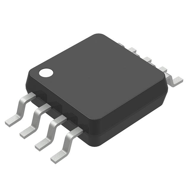


 工商网监
湘ICP备2023018690号
工商网监
湘ICP备2023018690号
