NCV8674
Linear Regulator - Low
Dropout, Very Low Iq
The NCV8674 is a precision 5.0 V or 12 V fixed output, low
dropout integrated voltage regulator with an output current
capability of 350 mA. Careful management of light load current
consumption, combined with a low leakage process, achieve a
typical quiescent current of 30 mA.
The output voltage is accurate within "2.0%, and maximum
dropout voltage is 600 mV at full rated load current.
It is internally protected against input supply reversal, output
overcurrent faults, and excess die temperature. No external
components are required to enable these features.
•
•
•
•
5.0 V and 12 V Output Voltage Options
"2.0% Output Accuracy, Over Full Temperature Range
40 mA Maximum Quiescent Current at IOUT = 100 mA
600 mV Maximum Dropout Voltage at 350 mA Load Current
Wide Input Voltage Operating Range of 5.5 V to 45 V
Internal Fault Protection
♦ −42 V Reverse Voltage
♦ Short Circuit/Overcurrent
♦ Thermal Overload
NCV Prefix for Automotive and Other Applications Requiring Site
and Control Changes
AEC−Q100 Qualified
EMC Compliant
This is a Pb−Free Device
© Semiconductor Components Industries, LLC, 2011
October, 2019− Rev. 3
MARKING
DIAGRAMS
4
1 2
Features
•
•
•
•
•
•
http://onsemi.com
1
NC
V8674xxx
AWLYWWG
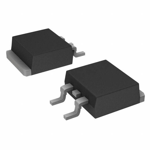
D2PAK
DS SUFFIX
CASE 936
3
1
xxx
A
WL
Y
WW
G
= 50 (5.0 V Option)
= 120 (12 V Option)
= Assembly Location
= Wafer Lot
= Year
= Work Week
= Pb−Free Package
PIN CONNECTIONS
PIN
1
2, TAB
3
FUNCTION
VIN
GND
VOUT
ORDERING INFORMATION
See detailed ordering and shipping information in the package
dimensions section on page 10 of this data sheet.
Publication Order Number:
NCV8674/D
�NCV8674
VIN
VOUT
Bias Current
Generators
1.3 V
Reference
+
Error
Amp
-
Thermal
Shutdown
GND
Figure 1. Block Diagram
PIN FUNCTION DESCRIPTION
Pin No.
Symbol
Function
1
VIN
2
GND
Ground; substrate.
3
VOUT
Regulated output voltage; collector of the internal PNP pass transistor.
TAB
GND
Ground; substrate and best thermal connection to the die.
Unregulated input voltage; (VOUT + 0.5 V) to 45 V.
OPERATING RANGE
Pin Symbol, Parameter
Symbol
Min
Max
Unit
VIN, DC Input Operating Voltage
VIN
VOUT + 0.5 V
+45
V
Junction Temperature Operating Range
TJ
−40
+150
_C
Symbol
Min
Max
Unit
VIN
−42
+45
V
VOUT
−0.3
+16
V
Tstg
−55
+150
_C
ESD Capability, Human Body Model (Note 1)
VESDHB
4000
−
V
ESD Capability, Machine Model (Note 1)
VESDMIM
200
−
V
MAXIMUM RATINGS
Rating
VIN, DC Voltage
VOUT, DC Voltage
Storage Temperature
Stresses exceeding Maximum Ratings may damage the device. Maximum Ratings are stress ratings only. Functional operation above the
Recommended Operating Conditions is not implied. Extended exposure to stresses above the Recommended Operating Conditions may affect
device reliability.
1. This device series incorporates ESD protection and is tested by the following methods:
ESD HBM tested per AEC−Q100−002 (EIA/JESD22−A 114C)
ESD MM tested per AEC−Q100−003 (EIA/JESD22−A 115C)
Thermal Resistance
Parameter
Symbol
Min
Max
Unit
Junction−to−Ambient (Note 2)
RqJA
−
40
°C/W
Junction−to−Case
RqJC
−
4.0
°C/W
2. 1 oz., 1
in2
copper area.
http://onsemi.com
2
�NCV8674
LEAD SOLDERING TEMPERATURE & MSL
Rating
Symbol
Min
Max
Unit
Lead Temperature Soldering − Reflow (SMD Styles Only), Lead Free (Note 3)
Tsld
−
265 pk
_C
Moisture Sensitivity Level
MSL
1
−
3. Lead Free, 60 sec – 150 sec above 217_C, 40 sec max at peak.
ELECTRICAL CHARACTERISTICS (VIN = 13.5 V, Tj = −40_C to +150_C, unless otherwise noted.)
Characteristic
Output Voltage
5 V Option
12 V Option
Line Regulation
5 V Option
12 V Option
Load Regulation
5 V Option
12 V Option
Dropout Voltage
Quiescent Current
5 V Option
12 V Option
Symbol
Test Conditions
Min
Typ
Max
VOUT
0.1 mA v IOUT v 350 mA (Note 4)
(VOUT + 1 V) v VIN v 28 V
4.90
11.76
5.00
12.00
5.10
12.24
DVOUT vs. VIN
IOUT = 5.0 mA
(VOUT + 1 V) v VIN v 28 V
−25
−60
5.0
12
+25
+60
DVOUT vs. IOUT
1.0 mA v IOUT v 350 mA
(Note 4)
−35
−84
5.0
12
+35
+84
VIN−VOUT
IOUT = 100 mA (Notes 4 & 5)
IOUT = 350 mA (Notes 4 & 5)
−
−
175
300
500
600
Iq
IOUT = 100 mA
TJ = 25_C
TJ = 25_C
−
−
27
31
35
39
TJ = −40_C to +85_C
TJ = −40_C to +85_C
−
−
30
34
38
42
IOUT = 50 mA (Note 4)
IOUT = 50 mA (Note 4)
−
−
1.1
1.1
3.0
3.0
IOUT = 350 mA (Note 4)
IOUT = 350 mA (Note 4)
−
−
18
21
27
40
5 V Option
12 V Option
Active Ground Current
5 V Option
12 V Option
IG(ON)
5 V Option
12 V Option
Unit
V
mV
mV
mV
mA
mA
Power Supply Rejection
PSRR
VRIPPLE = 0.5 VP−P, F = 100 Hz
−
67
−
dB
Output Capacitor for Stability
COUT
ESR
IOUT = 0.1 mA to 350 mA
(Note 4)
22
−
−
−
−
7.0
mF
W
VOUT = 4.5 V (Note 4)
VOUT = 10.8 V (Note 4)
350
350
−
−
−
−
IOUT(SC)
VOUT = 0 V (Note 4)
100
600
−
mA
TTSD
(Note 6)
150
−
200
_C
PROTECTION
Current Limit
5 V Option
12 V Option
Short Circuit Current Limit
Thermal Shutdown Threshold
IOUT(LIM)
mA
4. Use pulse loading to limit power dissipation.
5. Dropout voltage = (VIN – VOUT), measured when the output voltage has dropped 100 mV relative to the nominal value obtained with VIN = 13.5 V.
6. Not tested in production. Limits are guaranteed by design.
http://onsemi.com
3
�NCV8674
IIN
Input
CIN
1.0 mF
Vin
1
100 nF
8674
3
IOUT
Vout
Output
COUT
22 mF
2
RL
Iq
GND
Figure 2. Measurement Circuit
Vin
Input
CIN
100 nF
1
8674
3
Vout
Output
COUT
22 mF
2
Iq
GND
Figure 3. Applications Circuit
http://onsemi.com
4
�NCV8674
TYPICAL CHARACTERISTIC CURVES − 5 V OPTION
100
5.08
Unstable Region
1
Stable Region
0.1
Cout = 22 mF
TA = −40°C to 150°C
0.01
0.001
0
Unexplored Region*
100
150
200
250
OUTPUT CURRENT (mA)
50
Vout(nom) = 5.0 V
5.06
OUTPUT VOLTAGE (V)
10
ESR (W)
5.10
Vout(nom) = 5.0 V
300
5.04
5.02
5.00
4.98
4.96
4.94
4.90
−40 −20
350
CURRENT LIMIT (mA)
QUIESCENT CURRENT (mA)
70
60
50
40
30
20
Vin = 13.5 V
Iout = 100 mA
20
40
60
80
100 120
100 120
140 160
800
700
600
500
400
300
200
100
0
−40 −20
140 160
Vin = 6 V
0
20
40
60
80
100 120
140 160
TEMPERATURE (°C)
Figure 7. Current Limit vs. Temperature
Figure 6. Quiescent Current vs. Temperature
7
30
QUIESCENT CURRENT (mA)
Vout(nom) = 5.0 V
6
OUTPUT VOLTAGE (V)
80
Vout(nom) = 5.0 V
TEMPERATURE (°C)
5
4
3
2
1
0
60
900
80
0
40
1000
Vout(nom) = 5.0 V
0
−40 −20
20
Figure 5. Output Voltage vs. Temperature
*The min specified ESR is based on Murata’s capacitor
GRM31CR60J226KE19 used in measurement. The true
100 min ESR limit might be lower than shown.
10
0
TEMPERATURE (°C)
Figure 4. ESR Stability Region vs. Output
Current
90
Vin = 6 V
Iout = 100 mA
4.92
0
5
10
15
20
25
30
35
40
125°C
20
25°C
15
−40°C
10
5
0
45
Vout(nom) = 5.0 V
25
Vin = 13.5 V
0
INPUT VOLTAGE (V)
100
200
300
400
OUTPUT LOAD (mA)
Figure 8. Output Voltage vs. Input Voltage
Figure 9. Quiescent Current vs. Output Load
http://onsemi.com
5
�NCV8674
TYPICAL CHARACTERISTIC CURVES − 5 V OPTION
500
25
Vout(nom) = 5.0 V
QUIESCENT CURRENT (mA)
Vout(nom) = 5.0 V
400
350
Iout = 350 mA
300
250
200
Iout = 100 mA
150
100
50
0
−40 −20
0
20
40
60
80
100 120
20
15
10
5
0
−40 −20
140 160
Vin = 13.5 V
Iout = 350 mA
0
20
TEMPERATURE (°C)
40
60
80
100 120
140 160
TEMPERATURE (°C)
Figure 10. Dropout Voltage vs. Temperature
Figure 11. Quiescent Current vs. Temperature
− 350 mA Load
1.4
QUIESCENT CURRENT (mA)
DROPOUT VOLTAGE (mV)
450
1.2
Vout(nom) = 5.0 V
1.0
0.8
0.6
0.4
Vin = 13.5 V
Iout = 50 mA
0.2
0
−40 −20
0
20
40
60
80
100 120
140 160
TEMPERATURE (°C)
Figure 12. Quiescent Current vs. Temperature −
50 mA Load
Vin = 13.5 V
Iout = 100 mA
Cout = 22 mF
TA = 25°C
Vin = 13.5 V
Iout = 350 mA
Cout = 22 mF
TA = 25°C
Vout(nom) = 5.0 V
Figure 13. Power Supply Rejection − 100 mA
Vout(nom) = 5.0 V
Figure 14. Power Supply Rejection − 350 mA
http://onsemi.com
6
�NCV8674
TYPICAL CHARACTERISTIC CURVES − 12 V OPTION
100
12.20
Unstable Region
1
Stable Region
0.1
Cout = 22 mF
TA = −40°C to 150°C
0.01
0.001
0
Unexplored Region*
100
150
200
250
OUTPUT CURRENT (mA)
50
Vout(nom) = 12 V
12.15
OUTPUT VOLTAGE (V)
10
ESR (W)
12.25
Vout(nom) = 12 V
300
12.10
12.05
12.00
11.95
11.90
11.85
11.75
−40 −20
350
CURRENT LIMIT (mA)
QUIESCENT CURRENT (mA)
70
60
50
40
30
20
Vin = 13.5 V
Iout = 100 mA
0
20
40
60
80
100 120
100 120
140 160
Vout(nom) = 12 V
700
600
500
400
300
200
100
0
−40 −20
140 160
Vin = 13.5 V
0
20
40
60
80
100 120
140 160
TEMPERATURE (°C)
Figure 18. Current Limit vs. Temperature
Figure 17. Quiescent Current vs. Temperature
14
35
QUIESCENT CURRENT (mA)
Vout(nom) = 12 V
12
OUTPUT VOLTAGE (V)
80
800
TEMPERATURE (°C)
10
8
6
4
2
0
60
900
80
0
−40 −20
40
1000
Vout(nom) = 12 V
10
20
Figure 16. Output Voltage vs. Temperature
*The min specified ESR is based on Murata’s capacitor
GRM32ER71C226ME18 used in measurement. The true
min ESR limit might be lower than shown.
90
0
TEMPERATURE (°C)
Figure 15. ESR Stability Region vs. Output
Current
100
Vin = 13.5 V
Iout = 100 mA
11.80
0
5
10
15
20
25
30
35
40
125°C
25
25°C
20
−40°C
15
10
5
0
45
Vout(nom) = 12 V
30
Vin = 13.5 V
0
INPUT VOLTAGE (V)
100
200
300
400
OUTPUT LOAD (mA)
Figure 19. Output Voltage vs. Input Voltage
Figure 20. Quiescent Current vs. Output Load
http://onsemi.com
7
�NCV8674
TYPICAL CHARACTERISTIC CURVES − 12 V OPTION
500
35
QUIESCENT CURRENT (mA)
Vout(nom) = 12 V
400
Iout = 350 mA
350
300
250
Iout = 100 mA
200
150
100
50
0
−40 −20
0
20
40
60
80
100 120
Vout(nom) = 12 V
30
25
20
15
10
0
−40 −20
140 160
Vin = 13.5 V
Iout = 350 mA
5
0
20
TEMPERATURE (°C)
40
60
80
100 120
140 160
TEMPERATURE (°C)
Figure 21. Dropout Voltage vs. Temperature
Figure 22. Quiescent Current vs. Temperature
− 350 mA Load
1.8
1.6
QUIESCENT CURRENT (mA)
DROPOUT VOLTAGE (mV)
450
Vout(nom) = 12 V
1.4
1.2
1.0
0.8
0.6
0.4
Vin = 13.5 V
Iout = 50 mA
0.2
0
−40 −20
0
20
40
60
80
100 120
140 160
TEMPERATURE (°C)
Figure 23. Quiescent Current vs. Temperature −
50 mA Load
Figure 24. Power Supply Rejection − 100 mA
Figure 25. Power Supply Rejection − 350 mA
http://onsemi.com
8
�NCV8674
Circuit Description
must be paid to ESR constraints. The aluminum
electrolytic capacitor is the least expensive solution, but, if
the circuit operates at low temperatures (−25°C to −40°C),
both the value and ESR of the capacitor will vary
considerably. The capacitor manufacturer’s data sheet
usually provides this information. The value for the output
capacitor COUT shown in Figure 2 should work for most
applications; however, it is not necessarily the optimized
solution. Stability is guaranteed at values COUT ≥ 22 mF and
ESR ≤ 7.0 W, within the operating temperature range.
Actual limits are shown in a graph in the Typical
Characteristics section.
The NCV8674 is a precision trimmed 5.0 V or 12 V fixed
output regulator. Careful management of light load
consumption combined with a low leakage process results
in a typical quiescent current of 30 mA. The device has
current capability of 350 mA, with 600 mV of dropout
voltage at full rated load current. The regulation is provided
by a PNP pass transistor controlled by an error amplifier
with a bandgap reference. The regulator is protected by
both current limit and short circuit protection. Thermal
shutdown occurs above 150°C to protect the IC during
overloads and extreme ambient temperatures.
Regulator
Calculating Power Dissipation in a Single Output
Linear Regulator
The error amplifier compares the reference voltage to a
sample of the output voltage (Vout) and drives the base of
a PNP series pass transistor by a buffer. The reference is a
bandgap design to give it a temperature−stable output.
Saturation control of the PNP is a function of the load
current and input voltage. Over saturation of the output
power device is prevented, and quiescent current in the
ground pin is minimized. The NCV8674 is equipped with
foldback current protection. This protection is designed to
reduce the current limit during an overcurrent situation.
The maximum power dissipation for a single output
regulator (Figure 2) is:
PD(max) + [VIN(max) * VOUT(min)] @
IOUT(max) ) VIN(max) @ Iq
Where:
VIN(max) is the maximum input voltage,
VOUT(min) is the minimum output voltage,
IOUT(max) is the maximum output current for the
application, and Iq is the quiescent current the regulator
consumes at IOUT(max).
Once the value of PD(Max) is known, the maximum
permissible value of RqJA can be calculated:
Regulator Stability Considerations
RqJA +
150 oC * TA
PD
(eq. 2)
The value of RqJA can then be compared with those in
thermal resistance versus copper area graph (Figure 26).
Those designs with cooling area corresponding to RqJA’s
less than the calculated value in Equation 2 will keep the
die temperature below 150°C. The current flow and
voltages are shown in the Measurement Circuit Diagram.
100
75
50
R(t), (°C/W)
THERMAL RESISTANCE JUNCTION−TO−AIR
(°C/W)
The input capacitor CIN in Figure 2 is necessary for
compensating input line reactance. Possible oscillations
caused by input inductance and input capacitance can be
damped by using a resistor of approximately 1 W in series
with CIN. The output or compensation capacitor, COUT
helps determine three main characteristics of a linear
regulator: startup delay, load transient response and loop
stability. The capacitor value and type should be based on
cost, availability, size and temperature constraints.
Tantalum, aluminum electrolytic, film, or ceramic
capacitors are all acceptable solutions, however, attention
D2PAK 1 oz
D2PAK 2 oz
25
0
(eq. 1)
0
100
200
300
400
500
600
700
800
900
10
D2PAK
1
0.1
0.000001
COPPER AREA (mm2)
Single Pulse
0.0001
0.01
0.1
1
10
100 1000
PULSE TIME (sec)
Figure 27. NCV8674 @ PCB Cu Area 650 mm2
PCB Cu thk 1 oz
Figure 26.
http://onsemi.com
9
�NCV8674
ORDERING INFORMATION
Marking
Package
Shipping†
NCV8674DS50G
V867450
D2PAK
(Pb−Free)
50 Units / Rail
NCV8674DS50R4G
V867450
D2PAK
(Pb−Free)
800 / Tape & Reel
NCV8674DS120G
V8674120
D2PAK
(Pb−Free)
50 Units / Rail
NCV8674DS120R4G
V8674120
D2PAK
(Pb−Free)
800 / Tape & Reel
Device
†For information on tape and reel specifications, including part orientation and tape sizes, please refer to our Tape and Reel Packaging Specification
Brochure, BRD8011/D.
http://onsemi.com
10
�MECHANICAL CASE OUTLINE
PACKAGE DIMENSIONS
D2PAK
CASE 936−03
ISSUE E
DATE 29 SEP 2015
SCALE 1:1
T
C
A
K
B
J
C
ES
OPTIONAL
CHAMFER
DETAIL C
DETAIL C
3
F
G
SIDE VIEW
2X
TOP VIEW
D
0.010 (0.254)
N
DUAL GAUGE
CONSTRUCTION
P
BOTTOM VIEW
SIDE VIEW
SINGLE GAUGE
CONSTRUCTION
T
M
M
R
T
V
H
2
U
ED
OPTIONAL
CHAMFER
S
1
TERMINAL 4
T
SEATING
PLANE
L
BOTTOM VIEW
DETAIL C
OPTIONAL CONSTRUCTIONS
NOTES:
1. DIMENSIONING AND TOLERANCING PER ANSI
Y14.5M, 1982.
2. CONTROLLING DIMENSION: INCHES.
3. TAB CONTOUR OPTIONAL WITHIN DIMENSIONS
A AND K.
4. DIMENSIONS U AND V ESTABLISH A MINIMUM
MOUNTING SURFACE FOR TERMINAL 4.
5. DIMENSIONS A AND B DO NOT INCLUDE MOLD
FLASH OR GATE PROTRUSIONS. MOLD FLASH
AND GATE PROTRUSIONS NOT TO EXCEED
0.025 (0.635) MAXIMUM.
6. SINGLE GAUGE DESIGN WILL BE SHIPPED AF
TER FPCN EXPIRATION IN OCTOBER 2011.
DIM
A
B
C
D
ED
ES
F
G
H
J
K
L
M
N
P
R
S
U
V
INCHES
MIN
MAX
0.386
0.403
0.356
0.368
0.170
0.180
0.026
0.036
0.045
0.055
0.018
0.026
0.051 REF
0.100 BSC
0.539
0.579
0.125 MAX
0.050 REF
0.000
0.010
0.088
0.102
0.018
0.026
0.058
0.078
0_
8_
0.116 REF
0.200 MIN
0.250 MIN
MILLIMETERS
MIN
MAX
9.804 10.236
9.042
9.347
4.318
4.572
0.660
0.914
1.143
1.397
0.457
0.660
1.295 REF
2.540 BSC
13.691 14.707
3.175 MAX
1.270 REF
0.000
0.254
2.235
2.591
0.457
0.660
1.473
1.981
0_
8_
2.946 REF
5.080 MIN
6.350 MIN
GENERIC
MARKING DIAGRAM*
SOLDERING FOOTPRINT*
10.490
XXXXXXG
ALYWW
8.380
16.155
XXXXXX = Specific Device Code
A
= Assembly Location
L
= Wafer Lot
Y
= Year
WW
= Work Week
G
= Pb−Free Package
2X
3.504
2X
1.016
5.080
PITCH
DIMENSIONS: MILLIMETERS
*For additional information on our Pb−Free strategy and soldering
details, please download the ON Semiconductor Soldering and
Mounting Techniques Reference Manual, SOLDERRM/D.
DOCUMENT NUMBER:
DESCRIPTION:
98ASH01005A
D2PAK
*This information is generic. Please refer to
device data sheet for actual part marking.
Pb−Free indicator, “G” or microdot “ G”,
may or may not be present.
Electronic versions are uncontrolled except when accessed directly from the Document Repository.
Printed versions are uncontrolled except when stamped “CONTROLLED COPY” in red.
PAGE 1 OF 1
ON Semiconductor and
are trademarks of Semiconductor Components Industries, LLC dba ON Semiconductor or its subsidiaries in the United States and/or other countries.
ON Semiconductor reserves the right to make changes without further notice to any products herein. ON Semiconductor makes no warranty, representation or guarantee regarding
the suitability of its products for any particular purpose, nor does ON Semiconductor assume any liability arising out of the application or use of any product or circuit, and specifically
disclaims any and all liability, including without limitation special, consequential or incidental damages. ON Semiconductor does not convey any license under its patent rights nor the
rights of others.
© Semiconductor Components Industries, LLC, 2019
www.onsemi.com
�onsemi,
, and other names, marks, and brands are registered and/or common law trademarks of Semiconductor Components Industries, LLC dba “onsemi” or its affiliates
and/or subsidiaries in the United States and/or other countries. onsemi owns the rights to a number of patents, trademarks, copyrights, trade secrets, and other intellectual property.
A listing of onsemi’s product/patent coverage may be accessed at www.onsemi.com/site/pdf/Patent−Marking.pdf. onsemi reserves the right to make changes at any time to any
products or information herein, without notice. The information herein is provided “as−is” and onsemi makes no warranty, representation or guarantee regarding the accuracy of the
information, product features, availability, functionality, or suitability of its products for any particular purpose, nor does onsemi assume any liability arising out of the application or use
of any product or circuit, and specifically disclaims any and all liability, including without limitation special, consequential or incidental damages. Buyer is responsible for its products
and applications using onsemi products, including compliance with all laws, regulations and safety requirements or standards, regardless of any support or applications information
provided by onsemi. “Typical” parameters which may be provided in onsemi data sheets and/or specifications can and do vary in different applications and actual performance may
vary over time. All operating parameters, including “Typicals” must be validated for each customer application by customer’s technical experts. onsemi does not convey any license
under any of its intellectual property rights nor the rights of others. onsemi products are not designed, intended, or authorized for use as a critical component in life support systems
or any FDA Class 3 medical devices or medical devices with a same or similar classification in a foreign jurisdiction or any devices intended for implantation in the human body. Should
Buyer purchase or use onsemi products for any such unintended or unauthorized application, Buyer shall indemnify and hold onsemi and its officers, employees, subsidiaries, affiliates,
and distributors harmless against all claims, costs, damages, and expenses, and reasonable attorney fees arising out of, directly or indirectly, any claim of personal injury or death
associated with such unintended or unauthorized use, even if such claim alleges that onsemi was negligent regarding the design or manufacture of the part. onsemi is an Equal
Opportunity/Affirmative Action Employer. This literature is subject to all applicable copyright laws and is not for resale in any manner.
PUBLICATION ORDERING INFORMATION
LITERATURE FULFILLMENT:
Email Requests to: orderlit@onsemi.com
onsemi Website: www.onsemi.com
◊
TECHNICAL SUPPORT
North American Technical Support:
Voice Mail: 1 800−282−9855 Toll Free USA/Canada
Phone: 011 421 33 790 2910
Europe, Middle East and Africa Technical Support:
Phone: 00421 33 790 2910
For additional information, please contact your local Sales Representative
�


 工商网监
湘ICP备2023018690号
工商网监
湘ICP备2023018690号
