ON Semiconductor
Is Now
To learn more about onsemi™, please visit our website at
www.onsemi.com
onsemi and and other names, marks, and brands are registered and/or common law trademarks of Semiconductor Components Industries, LLC dba “onsemi” or its affiliates and/or
subsidiaries in the United States and/or other countries. onsemi owns the rights to a number of patents, trademarks, copyrights, trade secrets, and other intellectual property. A listing of onsemi
product/patent coverage may be accessed at www.onsemi.com/site/pdf/Patent-Marking.pdf. onsemi reserves the right to make changes at any time to any products or information herein, without
notice. The information herein is provided “as-is” and onsemi makes no warranty, representation or guarantee regarding the accuracy of the information, product features, availability, functionality,
or suitability of its products for any particular purpose, nor does onsemi assume any liability arising out of the application or use of any product or circuit, and specifically disclaims any and all
liability, including without limitation special, consequential or incidental damages. Buyer is responsible for its products and applications using onsemi products, including compliance with all laws,
regulations and safety requirements or standards, regardless of any support or applications information provided by onsemi. “Typical” parameters which may be provided in onsemi data sheets and/
or specifications can and do vary in different applications and actual performance may vary over time. All operating parameters, including “Typicals” must be validated for each customer application
by customer’s technical experts. onsemi does not convey any license under any of its intellectual property rights nor the rights of others. onsemi products are not designed, intended, or authorized
for use as a critical component in life support systems or any FDA Class 3 medical devices or medical devices with a same or similar classification in a foreign jurisdiction or any devices intended for
implantation in the human body. Should Buyer purchase or use onsemi products for any such unintended or unauthorized application, Buyer shall indemnify and hold onsemi and its officers, employees,
subsidiaries, affiliates, and distributors harmless against all claims, costs, damages, and expenses, and reasonable attorney fees arising out of, directly or indirectly, any claim of personal injury or death
associated with such unintended or unauthorized use, even if such claim alleges that onsemi was negligent regarding the design or manufacture of the part. onsemi is an Equal Opportunity/Affirmative
Action Employer. This literature is subject to all applicable copyright laws and is not for resale in any manner. Other names and brands may be claimed as the property of others.
�Buffer with Open Drain
Output
NL17SG07
The NL17SG07 MiniGatet is an advanced high−speed CMOS
Buffer with Open Drain Output in ultra−small footprint.
The NL17SG07 input structures provides protection when voltages
up to 5.5 V are applied with VCC greater than or equal to 0.9 volts,
otherwise the protection is up to 4.6 volts regardless of the supply
voltage.
www.onsemi.com
MARKING
DIAGRAMS
Features
Wide Operating VCC Range: 0.9 V to 3.6 V
SOT−953
CASE 527AE
High Speed: tPD = 2.5 ns (Typ) at VCC = 3.0 V, CL = 15 pF
Low Power Dissipation: ICC = 0.5 mA (Max) at TA = 25°C
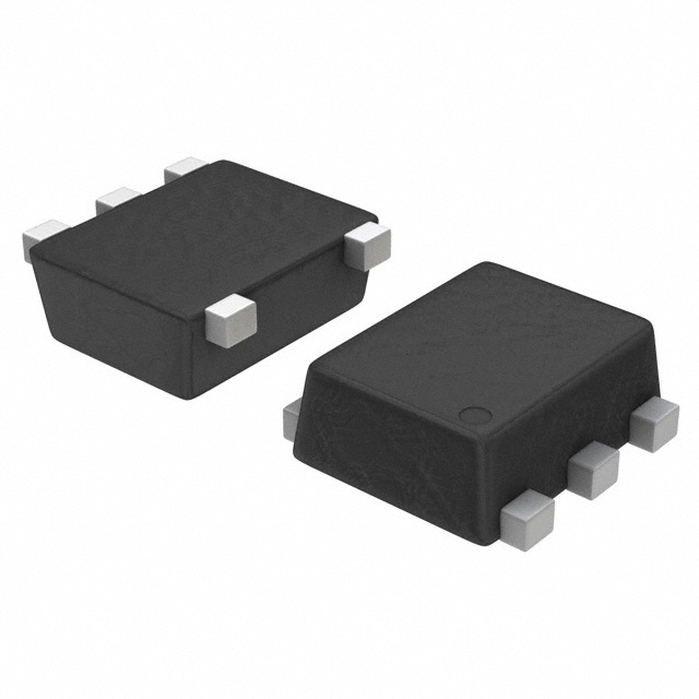
UDFN6
1.0 x 1.0
CASE 517BX
5.5 V Overvoltage Tolerant (OVT) Input Pins (VCC ≥ 0.9 V)
Ultra−Small Packages
These are Pb−Free and Halide−Free Devices
GND
2
NC
3
5
4
VCC
OUT Y
NC
1
IN A
2
GND
3
Figure 1. SOT−953
(Top View)
5
4
NC
1
6
VCC
IN A
2
5
NC
GND
3
OUT Y
1
M
AQ M G
G
OUT Y
M
G
= Date Code*
= Pb−Free Package
(Note: Microdot may be in either location)
*Date Code orientation and/or position may vary
depending upon manufacturing location.
PIN ASSIGNMENT
Figure 3. UDFN
(Top View)
IN A
M
VCC
SC−88A
DF SUFFIX
CASE 419A
Figure 2. SC−88A
(Top View)
4
V
1
UDFN6
1.45 x 1.0
CASE 517AQ
M
IN A
6M
1
J
•
•
•
•
•
•
PIN
SOT−953
SC−88A
UDFN6
1
IN A
NC
NC
2
GND
IN A
IN A
3
NC
GND
GND
4
OUT Y
OUT Y
OUT Y
5
VCC
VCC
NC
6
−
−
VCC
OUT Y
FUNCTION TABLE
Figure 4. Logic Symbol
Input A
Output Y
L
H
L
Z
ORDERING INFORMATION
See detailed ordering and shipping information in the package
dimensions section on page 5 of this data sheet.
© Semiconductor Components Industries, LLC, 2014
February, 2020 − Rev. 7
1
Publication Order Number:
NL17SG07/D
�NL17SG07
MAXIMUM RATINGS
Symbol
Parameter
VCC
DC Supply Voltage
VIN
DC Input Voltage
VOUT
Value
Unit
−0.5 to +5.5
V
−0.5 to +5.5
−0.5 to +4.6
V
−0.5 to VCC + 0.5
V
VIN < GND
−20
mA
VOUT < GND
VCC ≥ 0.9 V
VCC < 0.9 V
DC Output Voltage
IIK
DC Input Diode Current
IOK
DC Output Diode Current
−20
mA
IOUT
DC Output Source/Sink Current
±20
mA
ICC
DC Supply Current per Supply Pin
±20
mA
IGND
DC Ground Current per Ground Pin
±20
mA
TSTG
Storage Temperature Range
−65 to +150
°C
260
°C
+150
°C
TL
Lead Temperature, 1 mm from Case for 10 Seconds
TJ
Junction Temperature Under Bias
MSL
Moisture Sensitivity
FR
Flammability Rating
VESD
ILATCHUP
Level 1
Oxygen Index: 28 to 34
ESD Withstand Voltage
UL 94 V−0 @ 0.125 in
Human Body Model (Note 2)
Machine Model (Note 3)
Latch−up Performance above VCC and below GND at 125°C (Note 4)
>2000
>100
V
±75
mA
Stresses exceeding those listed in the Maximum Ratings table may damage the device. If any of these limits are exceeded, device functionality
should not be assumed, damage may occur and reliability may be affected.
1. Measured with minimum pad spacing on an FR4 board, using 10 mm−by−1 inch, 2−ounce copper trace with no air flow.
2. Tested to EIA/JESD22−A114−A.
3. Tested to EIA/JESD22−A115−A.
4. Tested to EIA/JESD78.
RECOMMENDED OPERATING CONDITIONS
Symbol
Min
Max
Unit
VCC
Positive DC Supply Voltage
0.9
3.6
V
VIN
Digital Input Voltage
0.0
3.6
V
0.0
0.0
0.0
VCC
3.6
3.6
V
−55
+125
°C
0
10
ns/V
VOUT
TA
Dt / DV
Characteristics
Output Voltage
Output at High or Low State
Tri−State Mode (Note 5)
Power−Down Mode (VCC = 0 V)
Operating Temperature Range
Input Transition Rise or Fail Rate
VCC = 3.3 V ± 0.3 V
Functional operation above the stresses listed in the Recommended Operating Ranges is not implied. Extended exposure to stresses beyond
the Recommended Operating Ranges limits may affect device reliability.
5. Applicable to devices with outputs that may be tri−stated.
www.onsemi.com
2
�NL17SG07
DC ELECTRICAL CHARACTERISTICS
Symbol
VIH
VIL
VOL
Parameter
Condition
High−Level
Input Voltage
Low−Level
Input Voltage
Low−Level
Output Voltage
VIN =
VIH or
VIL
TA = 255C
−555C 3 TA 3 1255C
VCC
(V)
Min
0.9
VCC
VCC
1.1 to 1.3
0.70 x
VCC
0.70 x
VCC
1.4 to 1.6
0.65 x
VCC
0.65 x
VCC
1.65 to 1.95
0.65 x
VCC
0.65 x
VCC
2.3 to 2.7
1.7
1.7
3.0 to 3.6
2.0
Typ
Max
Min
Max
Unit
V
2.0
0.9
GND
GND
1.1 to 1.3
0.30 x
VCC
0.30 x
VCC
1.4 to 1.6
0.35 x
VCC
0.35 x
VCC
1.65 to 1.95
0.35 x
VCC
0.35 x
VCC
2.3 to 2.7
0.7
0.7
3.0 to 3.6
0.8
0.8
IOL = 20 mA
0.9
0.1
0.1
IOL = 0.3 mA
1.1 to 1.3
0.25 x
VCC
0.25 x
VCC
IOL = 1.7 mA
1.4 to 1.6
0.25 x
VCC
0.25 x
VCC
IOL = 3.0 mA
1.65 to 1.95
0.45
0.45
IOL = 4.0 mA
2.3 to 2.7
0.4
0.4
IOL = 8.0 mA
3.0 to 3.6
0.4
0.4
V
V
IIN
Input Leakage
Current
0 ≤ VIN ≤ 3.6 V
0 to 3.6
±0.1
±1.0
mA
ICC
Quiescent
Supply Current
VIN = VCC or GND
3.6
0.5
10
mA
Product parametric performance is indicated in the Electrical Characteristics for the listed test conditions, unless otherwise noted. Product
performance may not be indicated by the Electrical Characteristics if operated under different conditions.
www.onsemi.com
3
�NL17SG07
ÎÎÎÎÎÎÎÎÎÎÎÎÎÎÎÎÎÎÎÎÎÎÎÎÎÎÎÎÎÎÎÎÎ
ÎÎÎÎÎÎÎÎÎÎÎÎÎÎÎÎÎÎÎÎÎÎÎÎÎÎÎÎÎÎÎÎÎ
AC ELECTRICAL CHARACTERISTICS (Input tr = tf = 3.0 ns)
TA =
−555C to +1255C
TA = 255C
Symbol
Parameter
Test Condition
VCC (V)
Min
Typ
Max
Min
Max
Unit
tPZL
Propagation Delay,
Enable Time,
A to Y
CL = 10 pF,
R1 = RL = 5 kW
0.9
−
12
−
−
−
ns
1.1 to 1.3
−
5.5
6.8
−
8.8
CL = 15 pF,
R1 = RL = 5 kW
CL = 30 pF,
R1 = RL = 5 kW
tPLZ
Propagation Delay,
Disable Time,
A to Y
CL = 10 pF,
R1 = RL = 5 kW
CL = 15 pF,
R1 = RL = 5 kW
CL = 30 pF,
R1 = RL = 5 kW
1.4 to 1.6
−
4.0
5.7
−
7.3
1.65 to 1.95
−
3.3
3.9
−
5.9
2.3 to 2.7
−
2.7
3.3
−
4.5
3.0 to 3.6
−
2.4
2.9
−
3.7
0.9
−
12.5
−
−
−
1.1 to 1.3
−
5.8
7.0
−
9.0
1.4 to 1.6
−
4.1
6.0
−
7.4
1.65 to 1.95
−
3.4
4.0
−
6.2
2.3 to 2.7
−
2.8
3.4
−
4.6
3.0 to 3.6
−
2.5
3.0
−
3.7
0.9
−
13.2
−
−
−
1.1 to 1.3
−
6.2
7.4
−
9.4
1.4 to 1.6
−
4.5
6.2
−
7.6
1.65 to 1.95
−
3.5
4.2
−
6.4
2.3 to 2.7
−
3.0
3.6
−
4.7
3.0 to 3.6
−
2.6
3.1
−
3.9
0.9
−
8.0
−
−
−
1.1 to 1.3
−
6.5
10.9
−
11.5
1.4 to 1.6
−
5.2
7.2
−
8.3
1.65 to 1.95
−
4.9
7.0
−
7.8
2.3 to 2.7
−
3.8
6.5
−
7.3
3.0 to 3.6
−
3.5
6.2
−
6.8
0.9
−
11.1
−
−
−
1.1 to 1.3
−
9.0
13.4
−
14
1.4 to 1.6
−
7.9
10
−
10.8
1.65 to 1.95
−
7.6
9.5
−
10.5
2.3 to 2.7
−
6.3
7.8
−
10
3.0 to 3.6
−
6.0
7.2
−
9.3
0.9
−
16.2
−
−
−
1.1 to 1.3
−
14
18.4
−
20
1.4 to 1.6
−
13
15
−
16
1.65 to 1.95
−
12.5
14.5
−
15.8
2.3 to 2.7
−
11.2
13.5
−
15.4
3.0 to 3.6
−
11
13.2
−
14.3
ns
ns
ns
ns
ns
CIN
Input Capacitance
0 to 3.6
−
3
−
−
−
pF
CPD
Power Dissipation
Capacitance (Note 6)
0.9 to 3.6
−
4
−
−
−
pF
6. CPD is defined as the value of the internal equivalent capacitance which is calculated from the dynamic operating current consumption without
load. Average operating current can be obtained by the equation: ICC(OPR) = CPD � VCC � fin + ICC. CPD is used to determine the no−load
dynamic power consumption; PD = CPD � VCC2 � fin + ICC � VCC.
www.onsemi.com
4
�NL17SG07
A
VCC
50%
tPZL
Y
GND
tPLZ
HIGH
IMPEDANCE
50% VCC
10% VCC
Figure 5. Switching Waveform
VCC
R1
PULSE
GENERATOR
DUT
RT
CL
Test
Switch
tPZL
tPLZ
VCC x 2
VCC x 2
VCC
2
GND
RL
Figure 6. Test Circuit
ORDERING INFORMATION
Package
Shipping†
NL17SG07P5T5G
SOT−953
(Pb−Free)
8000 / Tape & Reel
NL17SG07DFT2G
SC−88A
(Pb−Free)
3000 / Tape & Reel
NL17SG07AMUTCG
UDFN6 1.45x1 mm
(Pb−Free)
3000 / Tape & Reel
NL17SG07CMUTBG*
UDFN6 1x1 mm
(Pb−Free)
3000 / Tape & Reel
NL17SG07MU3TBG*
UDFN6 1x1 mm
(Pb−Free)
3000 / Tape & Reel
Device
†For information on tape and reel specifications, including part orientation and tape sizes, please refer to our Tape and Reel Packaging
Specifications Brochure, BRD8011/D.
*In Development
www.onsemi.com
5
�NL17SG07
PACKAGE DIMENSIONS
SOT−953
CASE 527AE
ISSUE E
X
D
Y
PIN ONE
INDICATOR
5
NOTES:
1. DIMENSIONING AND TOLERANCING PER ASME
Y14.5M, 1994.
2. CONTROLLING DIMENSION: MILLIMETERS
3. MAXIMUM LEAD THICKNESS INCLUDES LEAD
FINISH. MINIMUM LEAD THICKNESS IS THE
MINIMUM THICKNESS OF THE BASE MATERIAL.
4. DIMENSIONS D AND E DO NOT INCLUDE MOLD
FLASH, PROTRUSIONS, OR GATE BURRS.
A
4
HE
E
1
2 3
DIM
A
b
C
D
E
e
HE
L
L2
L3
C
TOP VIEW
SIDE VIEW
e
L
5X
5X
L3
MILLIMETERS
MIN
NOM
MAX
0.34
0.37
0.40
0.10
0.15
0.20
0.07
0.12
0.17
0.95
1.00
1.05
0.75
0.80
0.85
0.35 BSC
0.95
1.00
1.05
0.175 REF
0.05
0.10
0.15
−−−
−−−
0.15
SOLDERING FOOTPRINT*
5X
0.35
5X
0.20
5X
L2
5X
BOTTOM VIEW
b
PACKAGE
OUTLINE
0.08 X Y
1.20
1
0.35
PITCH
DIMENSIONS: MILLIMETERS
*For additional information on our Pb−Free strategy and soldering
details, please download the ON Semiconductor Soldering and
Mounting Techniques Reference Manual, SOLDERRM/D.
www.onsemi.com
6
�NL17SG07
PACKAGE DIMENSIONS
UDFN6 1.0x1.0, 0.35P
CASE 517BX
ISSUE O
PIN ONE
REFERENCE
2X
NOTES:
1. DIMENSIONING AND TOLERANCING PER
ASME Y14.5M, 1994.
2. CONTROLLING DIMENSION: MILLIMETERS.
3. DIMENSION b APPLIES TO PLATED
TERMINAL AND IS MEASURED BETWEEN
0.15 AND 0.20 MM FROM TERMINAL TIP.
4. PACKAGE DIMENSIONS EXCLUSIVE OF
BURRS AND MOLD FLASH.
A B
D
ÉÉÉ
ÉÉÉ
E
0.10 C
2X
0.10 C
DIM
A
A1
A3
b
D
E
e
L
L1
TOP VIEW
A3
0.05 C
A
MILLIMETERS
MIN
MAX
0.45
0.55
0.00
0.05
0.13 REF
0.12
0.22
1.00 BSC
1.00 BSC
0.35 BSC
0.25
0.35
0.30
0.40
0.05 C
SIDE VIEW
A1
C
RECOMMENDED
SOLDERING FOOTPRINT*
SEATING
PLANE
5X
e
5X
0.48
L
6X
0.22
3
1
L1
1.18
6
4
BOTTOM VIEW
6X
b
0.10
M
C A B
0.05
M
C
0.53
1
PKG
OUTLINE
NOTE 3
0.35
PITCH
DIMENSIONS: MILLIMETERS
*For additional information on our Pb−Free strategy and soldering
details, please download the ON Semiconductor Soldering and
Mounting Techniques Reference Manual, SOLDERRM/D.
www.onsemi.com
7
�NL17SG07
PACKAGE DIMENSIONS
UDFN6 1.45x1.0, 0.5P
CASE 517AQ
ISSUE O
A
B
D
PIN ONE
REFERENCE
0.10 C
L1
ÉÉÉ
ÉÉÉ
ÉÉÉ
DETAIL A
E
OPTIONAL
CONSTRUCTIONS
DETAIL B
A1
SIDE VIEW
MOLD CMPD
OPTIONAL
CONSTRUCTIONS
A
0.05 C
DIM
A
A1
A2
b
D
E
e
L
L1
DETAIL B
0.05 C
6X
A2
6X
C
6X
SEATING
PLANE
0.30
PACKAGE
OUTLINE
L
1.24
3
1
DETAIL A
6X
0.53
4
BOTTOM VIEW
MILLIMETERS
MIN
MAX
0.45
0.55
0.00
0.05
0.07 REF
0.20
0.30
1.45 BSC
1.00 BSC
0.50 BSC
0.30
0.40
−−−
0.15
MOUNTING FOOTPRINT
e
6
NOTES:
1. DIMENSIONING AND TOLERANCING PER
ASME Y14.5M, 1994.
2. CONTROLLING DIMENSION: MILLIMETERS.
3. DIMENSION b APPLIES TO PLATED TERMINAL
AND IS MEASURED BETWEEN 0.15 AND
0.30 mm FROM THE TERMINAL TIP.
ÉÉ
ÉÉ
EXPOSED Cu
TOP VIEW
0.10 C
L
L
6X
0.50
PITCH
DIMENSIONS: MILLIMETERS
b
0.10 C A B
0.05 C
1
NOTE 3
*For additional information on our Pb−Free strategy and soldering
details, please download the ON Semiconductor Soldering and
Mounting Techniques Reference Manual, SOLDERRM/D.
www.onsemi.com
8
�NL17SG07
PACKAGE DIMENSIONS
SC−88A (SC−70−5/SOT−353)
CASE 419A−02
ISSUE L
A
G
5
4
−B−
S
1
2
NOTES:
1. DIMENSIONING AND TOLERANCING
PER ANSI Y14.5M, 1982.
2. CONTROLLING DIMENSION: INCH.
3. 419A−01 OBSOLETE. NEW STANDARD
419A−02.
4. DIMENSIONS A AND B DO NOT INCLUDE
MOLD FLASH, PROTRUSIONS, OR GATE
BURRS.
DIM
A
B
C
D
G
H
J
K
N
S
3
D 5 PL
0.2 (0.008)
B
M
M
N
INCHES
MIN
MAX
0.071
0.087
0.045
0.053
0.031
0.043
0.004
0.012
0.026 BSC
--0.004
0.004
0.010
0.004
0.012
0.008 REF
0.079
0.087
MILLIMETERS
MIN
MAX
1.80
2.20
1.15
1.35
0.80
1.10
0.10
0.30
0.65 BSC
--0.10
0.10
0.25
0.10
0.30
0.20 REF
2.00
2.20
J
C
K
H
SOLDER FOOTPRINT*
0.50
0.0197
0.65
0.025
0.65
0.025
0.40
0.0157
1.9
0.0748
SCALE 20:1
mm Ǔ
ǒinches
*For additional information on our Pb−Free strategy and soldering
details, please download the ON Semiconductor Soldering and
Mounting Techniques Reference Manual, SOLDERRM/D.
MiniGate is a trademark of Semiconductor Components Industries, LLC (SCILLC).
ON Semiconductor and
are trademarks of Semiconductor Components Industries, LLC dba ON Semiconductor or its subsidiaries in the United States and/or other countries.
ON Semiconductor owns the rights to a number of patents, trademarks, copyrights, trade secrets, and other intellectual property. A listing of ON Semiconductor’s product/patent
coverage may be accessed at www.onsemi.com/site/pdf/Patent−Marking.pdf. ON Semiconductor reserves the right to make changes without further notice to any products herein.
ON Semiconductor makes no warranty, representation or guarantee regarding the suitability of its products for any particular purpose, nor does ON Semiconductor assume any liability
arising out of the application or use of any product or circuit, and specifically disclaims any and all liability, including without limitation special, consequential or incidental damages.
Buyer is responsible for its products and applications using ON Semiconductor products, including compliance with all laws, regulations and safety requirements or standards,
regardless of any support or applications information provided by ON Semiconductor. “Typical” parameters which may be provided in ON Semiconductor data sheets and/or
specifications can and do vary in different applications and actual performance may vary over time. All operating parameters, including “Typicals” must be validated for each customer
application by customer’s technical experts. ON Semiconductor does not convey any license under its patent rights nor the rights of others. ON Semiconductor products are not
designed, intended, or authorized for use as a critical component in life support systems or any FDA Class 3 medical devices or medical devices with a same or similar classification
in a foreign jurisdiction or any devices intended for implantation in the human body. Should Buyer purchase or use ON Semiconductor products for any such unintended or unauthorized
application, Buyer shall indemnify and hold ON Semiconductor and its officers, employees, subsidiaries, affiliates, and distributors harmless against all claims, costs, damages, and
expenses, and reasonable attorney fees arising out of, directly or indirectly, any claim of personal injury or death associated with such unintended or unauthorized use, even if such
claim alleges that ON Semiconductor was negligent regarding the design or manufacture of the part. ON Semiconductor is an Equal Opportunity/Affirmative Action Employer. This
literature is subject to all applicable copyright laws and is not for resale in any manner.
PUBLICATION ORDERING INFORMATION
LITERATURE FULFILLMENT:
Literature Distribution Center for ON Semiconductor
19521 E. 32nd Pkwy, Aurora, Colorado 80011 USA
Phone: 303−675−2175 or 800−344−3860 Toll Free USA/Canada
Fax: 303−675−2176 or 800−344−3867 Toll Free USA/Canada
Email: orderlit@onsemi.com
◊
N. American Technical Support: 800−282−9855 Toll Free
USA/Canada
Europe, Middle East and Africa Technical Support:
Phone: 421 33 790 2910
www.onsemi.com
9
ON Semiconductor Website: www.onsemi.com
Order Literature: http://www.onsemi.com/orderlit
For additional information, please contact your local
Sales Representative
NL17SG07/D
�


 工商网监
湘ICP备2023018690号
工商网监
湘ICP备2023018690号
