NUP4301MR6T1 Low Capacitance Diode Array for ESD Protection in Four Data Lines
NUP4301MR6T1 is a MicroIntegrationt device designed to provide protection for sensitive components from possible harmful electrical transients; for example, ESD (electrostatic discharge).
Features http://onsemi.com
5 4 3
• Low Capacitance (1.5 pf Maximum Between I/O Lines) • Single Package Integration Design • Provides ESD Protection for JEDEC Standards JESD22 • • • • • • • • • • • • •
Machine Model = Class C Human Body Model = Class 3B Protection for IEC61000−4−2 (Level 4) 8.0 kV (Contact) 15 kV (Air) Ensures Data Line Speed and Integrity Fewer Components and Less Board Space Direct the Transient to Either Positive Side or to the Ground Pb−Free Package is Available USB 1.1 and 2.0 Data Line Protection T1/E1 Secondary IC Protection T3/E3 Secondary IC Protection HDSL, IDSL Secondary IC Protection Video Line Protection Microcontroller Input Protection Base Stations I2C Bus Protection
6
1
2
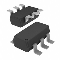
TSOP−6 CASE 318F PLASTIC
MARKING DIAGRAM
Applications
1
64M G G
64 = Device Code M = Date Code* G = Pb−Free Package (Note: Microdot may be in either location. *Date Code orientation may vary depending upon manufacturing location.
MAXIMUM RATINGS (Each Diode) (TJ = 25°C unless otherwise noted)
Rating Reverse Voltage Forward Current Peak Forward Surge Current Repetitive Peak Reverse Voltage Average Rectified Forward Current (Note 1) (averaged over any 20 ms period) Repetitive Peak Forward Current Non−Repetitive Peak Forward Current t = 1.0 ms t = 1.0 ms t = 1.0 S Symbol VR IF IFM(surge) VRRM IF(AV) Value 70 200 500 70 715 Unit Vdc
PIN CONFIGURATION AND SCHEMATIC
I/O 1 mAdc mAdc V mA VN 2 1/O 3
6 I/O 5 VP 4 I/O
IFRM IFSM
450 2.0 1.0 0.5
mA A
ORDERING INFORMATION
Device NUP4301MR6T1 NUP4301MR6T1G Package TSOP−6 TSOP−6 (Pb−Free) Shipping † 3000/Tape & Reel 3000/Tape & Reel
Maximum ratings are those values beyond which device damage can occur. Maximum ratings applied to the device are individual stress limit values (not normal operating conditions) and are not valid simultaneously. If these limits are exceeded, device functional operation is not implied, damage may occur and reliability may be affected. 1. FR−5 = 1.0 � 0.75 � 0.062 in.
© Semiconductor Components Industries, LLC, 2005
†For information on tape and reel specifications, including part orientation and tape sizes, please refer to our Tape and Reel Packaging Specifications Brochure, BRD8011/D. Publication Order Number: NUP4301MR6T1/D
1
September, 2005 − Rev. 3
�NUP4301MR6T1
THERMAL CHARACTERISTICS
Characteristic Thermal Resistance, Junction−to−Ambient Lead Solder Temperature, Maximum 10 Seconds Duration Junction Temperature Storage Temperature Symbol RqJA TL TJ Tstg Max 556 260 −40 to +85 −55 to +150 Unit °C/W °C °C °C
ELECTRICAL CHARACTERISTICS (TJ = 25°C unless otherwise noted) (Each Diode)
Characteristic OFF CHARACTERISTICS Reverse Breakdown Voltage (I(BR) = 100 mA) Reverse Voltage Leakage Current (VR = 70 Vdc) (VR = 25 Vdc, TJ = 150°C) (VR = 70 Vdc, TJ = 150°C) V(BR) IR 70 − − − − − − − − − − − − − 0.8 1.6 − − − − − 2.5 30 50 1.5 3 715 855 1000 1250 Vdc mAdc Symbol Min Typ Max Unit
Capacitance (between I/O pins) (VR = 0 V, f = 1.0 MHz) Capacitance (between I/O pin and ground) (VR = 0 V, f = 1.0 MHz) Forward Voltage (IF = 1.0 mAdc) (IF = 10 mAdc) (IF = 50 mAdc) (IF = 150 mAdc)
CD CD VF
pF pF mVdc
2. Alumina = 0.4 � 0.3 � 0.024 in. 99.5% alumina.
Curves Applicable to Each Cathode
100 IF, FORWARD CURRENT (mA) TA = 85°C 10 TA = −40°C IR , REVERSE CURRENT (μA) 10 TA = 150°C TA = 125°C
1.0
0.1
TA = 85°C TA = 55°C
1.0
TA = 25°C
0.01 TA = 25°C 0 10 20 30 40 VR, REVERSE VOLTAGE (VOLTS) 50
0.1
0.2
0.4
0.6 0.8 1.0 VF, FORWARD VOLTAGE (VOLTS)
1.2
0.001
Figure 1. Forward Voltage
1.75 CD, DIODE CAPACITANCE (pF)
Figure 2. Leakage Current
1.5
1.25
1.0
0.75
0
2 4 6 VR, REVERSE VOLTAGE (VOLTS)
8
Figure 3. Capacitance http://onsemi.com
2
�NUP4301MR6T1
PACKAGE DIMENSIONS
TSOP−6 CASE 318F−05 ISSUE L
D
6
5 1 2
4
HE
E
3
NOTES: 1. DIMENSIONING AND TOLERANCING PER ANSI Y14.5M, 1982. 2. CONTROLLING DIMENSION: INCH. 3. MAXIMUM LEAD THICKNESS INCLUDES LEAD FINISH THICKNESS. MINIMUM LEAD THICKNESS IS THE MINIMUM THICKNESS OF BASE MATERIAL. 4. 318F−01, −02, −03 OBSOLETE. NEW STANDARD 318F−04. DIM A A1 b c D E e L HE q MIN 0.90 0.01 0.25 0.10 2.90 1.30 0.85 0.20 2.50 0° MILLIMETERS NOM MAX 1.00 1.10 0.06 0.10 0.37 0.50 0.18 0.26 3.00 3.10 1.50 1.70 0.95 1.05 0.40 0.60 2.75 3.00 10° − MIN 0.035 0.001 0.010 0.004 0.114 0.051 0.034 0.008 0.099 0° INCHES NOM 0.039 0.002 0.015 0.007 0.118 0.059 0.037 0.016 0.108 − MAX 0.043 0.004 0.020 0.010 0.122 0.067 0.041 0.024 0.118 10°
b e q
0.05 (0.002) A1
A L
C
SOLDERING FOOTPRINT*
2.4 0.094
1.9 0.075
0.95 0.037 0.95 0.037
0.7 0.028 1.0 0.039
SCALE 10:1 mm inches
*For additional information on our Pb−Free strategy and soldering details, please download the ON Semiconductor Soldering and Mounting Techniques Reference Manual, SOLDERRM/D.
http://onsemi.com
3
�NUP4301MR6T1
MicroIntegration is a trademarks of Semiconductor Components Industries, LLC (SCILLC).
ON Semiconductor and are registered trademarks of Semiconductor Components Industries, LLC (SCILLC). SCILLC reserves the right to make changes without further notice to any products herein. SCILLC makes no warranty, representation or guarantee regarding the suitability of its products for any particular purpose, nor does SCILLC assume any liability arising out of the application or use of any product or circuit, and specifically disclaims any and all liability, including without limitation special, consequential or incidental damages. “Typical” parameters which may be provided in SCILLC data sheets and/or specifications can and do vary in different applications and actual performance may vary over time. All operating parameters, including “Typicals” must be validated for each customer application by customer’s technical experts. SCILLC does not convey any license under its patent rights nor the rights of others. SCILLC products are not designed, intended, or authorized for use as components in systems intended for surgical implant into the body, or other applications intended to support or sustain life, or for any other application in which the failure of the SCILLC product could create a situation where personal injury or death may occur. Should Buyer purchase or use SCILLC products for any such unintended or unauthorized application, Buyer shall indemnify and hold SCILLC and its officers, employees, subsidiaries, affiliates, and distributors harmless against all claims, costs, damages, and expenses, and reasonable attorney fees arising out of, directly or indirectly, any claim of personal injury or death associated with such unintended or unauthorized use, even if such claim alleges that SCILLC was negligent regarding the design or manufacture of the part. SCILLC is an Equal Opportunity/Affirmative Action Employer. This literature is subject to all applicable copyright laws and is not for resale in any manner.
PUBLICATION ORDERING INFORMATION
LITERATURE FULFILLMENT: N. American Technical Support: 800−282−9855 Toll Free Literature Distribution Center for ON Semiconductor USA/Canada P.O. Box 61312, Phoenix, Arizona 85082−1312 USA Phone: 480−829−7710 or 800−344−3860 Toll Free USA/Canada Japan : ON Semiconductor, Japan Customer Focus Center 2−9−1 Kamimeguro, Meguro−ku, Tokyo, Japan 153−0051 Fax: 480−829−7709 or 800−344−3867 Toll Free USA/Canada Phone: 81−3−5773−3850 Email: orderlit@onsemi.com ON Semiconductor Website: http://onsemi.com Order Literature: http://www.onsemi.com/litorder For additional information, please contact your local Sales Representative.
http://onsemi.com
4
NUP4301MR6T1/D
�


 工商网监
湘ICP备2023018690号
工商网监
湘ICP备2023018690号
