TVL-55738GD032J-LW-G-AAN 数据手册
R
RooHS
S
CO
OMP
PLLIA
AN
NT
T
APPROVAL SHEET
承
認
書
Customer
客戶名稱
Part No.
產品型號
TVL-55738GD032J-LW-G-AAN
Mode: Transmissive and Normally white type
Product type
產品內容
3.2” a-Si TFT LCD Module
RoHS
綠色產品
□ Non-compliance
■ Compliance
Remarks
備註欄
■Preliminary Specification 暫行 規格
□Final Specification 正 式規 格
Signature by Customer:
客戶確認簽章:
Issued by
QA
Checked by
QA
TVL-55738GD030AAN ver.B
Checked by
PM
-1-
Approved By
QA
RD
Issue Date: 2012/04/24
�R
RooHS
S
CO
OMP
PLLIA
AN
NT
T
Specification of LCD Module
Product No.: TVL-55738GD032J-LW-G-AAN
Issue date: 2012/04/24
KYOCERA DISPLAY CORPORATION
5-7-18, Higashinippori Arakawa-ku ,
Tokyo 116-0014, Japan
TEL: +81-3-5811-8780
FAX: +81-3-5811-8782
TVL-55738GD030AAN ver.B
-2-
Issue Date: 2012/04/24
�R
RooHS
S
CO
OMP
PLLIA
AN
NT
T
TABLE OF CONTENTS
1. GENERAL DESCRIPTION ..................................................................5
2. FEATURES ..........................................................................................5
3. MECHANICAL SPECIFICATION.........................................................5
4. MECHANICAL DIMENSION................................................................6
5. MAXIMUM RATINGS...........................................................................7
6. ELECTRICAL CHARACTERISTIC......................................................7
7. BACKLIGHT CHARACETRISTIC .......................................................8
8. MODULE FUNCTION DESCRIPTION.................................................9
8.1.
Pin Description ....................................................................................................9
8.2.
Timing Characteristics .......................................................................................11
8.3.
Serial Peripheral Interface (Spi).........................................................................12
8.4.
Block diagram of LCM.......................................................................................13
9. ELECTRO-OPTICAL CHARACTERISTICS......................................15
10. RELIABILITY......................................................................................17
10.1.
MTTF.................................................................................................................17
10.2.
Tests..................................................................................................................17
10.3.
Color performance.............................................................................................17
11. INSPECTION CRITERIA....................................................................18
11.1.
Inspection Conditions ........................................................................................18
11.2.
Light Method......................................................................................................18
11.3.
Classification Of Defects ...................................................................................19
11.4.
Sampling & Acceptable Quality Level................................................................19
11.5.
Definition Of Inspection Area.............................................................................19
11.6.
Items and Criteria ..............................................................................................20
12. ILLUSTRATION OF LCD DATE CODE.............................................22
TVL-55738GD030AAN ver.B
-3-
Issue Date: 2012/04/24
�R
RooHS
S
CO
OMP
PLLIA
AN
NT
T
13. RoHS COMPLIANT WARRANTY .....................................................23
14. PRECAUTIONS FOR USE ................................................................23
14.1.
Safety................................................................................................................23
14.2.
Storage Conditions............................................................................................23
14.3.
Installing LCD Module........................................................................................23
14.4.
Precautions For Operation ................................................................................24
14.5.
Handling Precautions ........................................................................................24
14.6.
Warranty............................................................................................................24
15. REVISION HISTORY .........................................................................25
TVL-55738GD030AAN ver.B
-4-
Issue Date: 2012/04/24
�R
RooHS
S
CO
OMP
PLLIA
AN
NT
T
1. GENERAL DESCRIPTION
TVL-55738GD032J-LW-G-AAN is a transmissive type color active matrix
liquid crystal display (LCD), which uses amorphous thin film transistor (TFT) as
switching devices. This product is composed of a TFT LCD panel, driver IC, and FPC,
backlight unit.
2. FEATURES
Display Mode
Transmissive Type
a-Si color TFT LCD, Normally white type
Screen Size
3.2 inches
Display Format
Graphic 320*RGB*240 Stripe type
Color Depth
16.7M colors
Input Data
24-bit Parallel RGB with SPI (3 wires) control interface
Viewing Direction
Higher Contrast ratio: 6 o’clock
Less gray scale reversal: 12 o’clock
Backlight
White LED
Driver IC
ILI9322B
3. MECHANICAL SPECIFICATION
Item
Specifications
Unit
Dimensional outline
70.36(W) × 58.96(H) ×3.3(D)*
mm
Resolution
320 × RGB × 240
Pixel
Active area
65.04(W) × 48.78(H)
mm
Pixel pitch
0.20325(W) × 0.20325(H)**
mm
Dots pitch
0.6775(W) × 0.20325(H)
mm
*Note: Not Including FPC length.
**Note: 1 pixel = 3 dots = Red dot +Green dot +Blue dot.
TVL-55738GD030AAN ver.B
-5-
Issue Date: 2012/04/24
�R
RooHS
S
CO
OMP
PLLIA
AN
NT
T
4. MECHANICAL DIMENSION
TVL-55738GD030AAN ver.B
-6-
Issue Date: 2012/04/24
�R
RooHS
S
CO
OMP
PLLIA
AN
NT
T
5. MAXIMUM RATINGS
If the operating condition exceeds the following absolute maximum ratings, the TFT
LCD module may be damaged permanently.
Items
Symbol Condition Min.
Max.
Unit
Note
VCI
AGND=0
-0.3
4.6
Volt
VDD
GND=0
-0.3
4.6
Operating Temperature
Top
-
-20
70
Volt
℃
Ambient temperature
Storage Temperature
Tst
-
-30
80
℃
Ambient temperature
Power Voltage
Humidity
90
%RH
Note:
1) All the voltages listed above are with respective to GND=0V。
2) Device is subject to be damaged permanently if stresses beyond those absolute
maximum ratings listed above。
3) Note1: TA≦40℃ Without dewing
6. ELECTRICAL CHARACTERISTIC
A. Typical operating conditions
Symbol
Min.
Typ.
Max.
Unit
VCI
2.7
3.3
3.6
V
VDD
1.65
3.3
3.6
V
IDD
--
10
20
mA
Output signal high voltage
VOH
0.8* VDD
-
VDD
V
Output signal low voltage
VOL
GND
-
0.2*VDD
V
Input signal high voltage
VIH
0.7* VDD
-
VDD
V
Input signal low voltage
VIL
GND
-
0.3*VDD
V
Items
Power Voltage
LCD driving current
TVL-55738GD030AAN ver.B
-7-
Note
Issue Date: 2012/04/24
�R
RooHS
S
CO
OMP
PLLIA
AN
NT
T
7. BACKLIGHT CHARACETRISTIC
ITEM
SYMBOL
Backlight power
VLED
supply
Backlight
ILED
current
CONDITION
Ta = 25℃
I = 20mA
Ta = 25℃
Min
Typ
Max
Units
9
---
11.1
V
---
20
---
mA
a. Test Instrument: BM-7 (Distance =500mm; Field = 1°)
b. Light Source: LED * 6 (White)
c. Conditions: VF = 9~11.1 V; IF = 20mA
d. Measure Brightness: 1 ~ 9
e. Uniformity = (Min. Brightness / Max. Brightness)*100%
f. Uniformity ≧ 70 %
Note:
The maximum difference between LED voltages |(A1-K1)-(A2-K2)| of a
single display shall be less than 1.0 V @ 20 mA 。
2W/3
W/3
H/3
2H/3
○
1
○
2
○
3
○
4
○
5
○
6
○
7
○
8
○
9
Active area
TVL-55738GD030AAN ver.B
-8-
A
c
t
i
v
e
a
r
e
a
(
H
)
Issue Date: 2012/04/24
�R
RooHS
S
CO
OMP
PLLIA
AN
NT
T
8. MODULE FUNCTION DESCRIPTION
8.1.Pin Description
Pin
Symbol
Description
1
LED A
LED Anode
2
LED A
LED Anode
3
LED K
LED Cathode
4
LED K
LED Cathode
5
GND
6
VCI
7
NC
8
VDD
Interface power supply = 1.65V~3.6V
9
GND
Ground
10
RESB
Chip reset Select Input PIN
Ground
A supply voltage to the analog circuit。Connect to an external
power supply of 2.7V~3.6V。
NC
A chip select signal。
11
CSB
CSB = L:the ILI9322 is selected and accessible
CSB = H:the ILI9322 is not selected and not accessible
Fix CSB to the IOVCC level when not in use。
12
13
SCK
SDO
SPI clock signal。
Fix SCK to GND level when not in use。
SPI interface output pin。
The data is outputted on the falling edge of the SCL signal。
Let SDO as floating when not used。
SPI interface input pin。
14
SDI
The data is latched on the rising edge of the SCL signal。
Fix SDI to GND level when not in use。
15
GND
Ground
16~23
B0~B7
TVL-55738GD030AAN ver.B
Graphic display Blue data
-9-
Issue Date: 2012/04/24
�R
RooHS
S
CO
OMP
PLLIA
AN
NT
T
24~31
G0~G7
Graphic display Green data
32~39
R0~R7
Graphic display Red data
40
GND
Ground
41
DCLK
Clock signal
The input data is latched on the rising edge of CLK。
42
43
HSYNC
VSYNC
Horizontal synchronizing input signal
When the ITU-R BT656 input interface is selected,this pin is
unused and short HSYNC pin to GND。
Vertical synchronizing input signal
When the ITU-R BT656 input interface is selected,this pin is
unused and short VSYNC pin to GND。
Input data enable signal
VSYNC+HSYNC mode:This pin is shorted to GND normally
and the back/front porch is determined by the control
register。
44
DEN
VSYNC+HSYNC+DE mode:The valid data is determined by
the VSYNC+HSYNC+DE pin。
DE mode:VSYNC and HSYNC are unused and shorted to
GND。The valid input data is determined by DE pin。
Fix DE to GND level when not in use。
45
GND
TVL-55738GD030AAN ver.B
Ground
- 10 -
Issue Date: 2012/04/24
�R
RooHS
S
CO
OMP
PLLIA
AN
NT
T
8.2.Timing Characteristics
8.2.1.24-bit parallel interface
TVL-55738GD030AAN ver.B
- 11 -
Issue Date: 2012/04/24
�R
RooHS
S
CO
OMP
PLLIA
AN
NT
T
8.3.Serial Peripheral Interface (Spi)
SPI Interface Input Signal Timing
TVL-55738GD030AAN ver.B
- 12 -
Issue Date: 2012/04/24
�R
RooHS
S
CO
OMP
PLLIA
AN
NT
T
8.4.Block diagram of LCM
TVL-55738GD030AAN ver.B
- 13 -
Issue Date: 2012/04/24
�R
RooHS
S
CO
OMP
PLLIA
AN
NT
T
TVL-55738GD030AAN ver.B
- 14 -
Issue Date: 2012/04/24
�R
RooHS
S
CO
OMP
PLLIA
AN
NT
T
9. ELECTRO-OPTICAL CHARACTERISTICS
Parameter
Symbol
Min.
Typ.
Max.
Units
Note
Luminance of white
Lwh
250
300
-
cd/m2
3
Contrast Ratio
CR
-
300
-
-
5
x
0.27
0.32
0.37
y
0.26
0.31
0.36
x
0.59
0.64
0.69
y
0.30
0.35
0.40
x
0.33
0.38
0.43
y
0.51
0.56
0.61
x
0.10
0.15
0.20
y
0.03
0.08
0.13
Tr+Tf
---
---
40
Y axis down
(12H)
ψL
50
55
---
Y axis up
(6H)
ψH
55
60
---
θR
60
65
---
θL
60
65
---
White
CIE color
Coordinates
Red
Green
Blue
Response Time
Viewing
Angle
(with Polarizer)
X axis right
(9H)
X axis left
(3H)
BM5;
-
1∘ angle
ms
4
Degree
5
Note:
1. Test equipment setup
After stabilizing and leaving the panel alone at a given temperature for 30
minutes, the measurement should be executed. Measurement should be
executed in a stable, windless, and dark room. Optical specifications are
measured by Topcon BM-5(fast) with a viewing angle of 1° at a distance of
50cm and normal direction.
TVL-55738GD030AAN ver.B
- 15 -
Issue Date: 2012/04/24
�R
RooHS
S
CO
OMP
PLLIA
AN
NT
T
2.
Definition of response time: TR and TF
The figure below is the output signal of the photo detector.
White
Display Area
Black
TR
100%
Optical
Response
White
TF
90%
10%
0%
Time
3.
Definition of contrast ratio:
Contrast ratio (CR) =
Brightness measured when LCD is at “white state”
Brightness measured when LCD is at “black state”
White Vi=Vi50%±1.5V
Black Vi=Vi50% 2.0V
”±” means that the analog input signal swings in phase with VCOM
signal.
” ” means that the analog input signal swings out of phase with VCOM
signal.
Vi50%: The analog input voltage when transmission is 50%.
The 100% transmission is defined as the transmission of LCD panel
when all the input terminals of module are electrically opened.
4.
Measured at the center area of the panel when all the input terminals of LCD
panel are electrically opened.
5. Definition of viewing angle:
N o rm a l lin e
θ 0 ;
0
L
Y axis up
R
1 2 o ’c lo c k d ire c tio n
L
H
90
H
X axis left
R ig h t
L e ft
L
90
To p
R
90
X axis right
B o tto m
6 o ’clo c k d ire c tio n
L
90
Y axis down
TVL-55738GD030AAN ver.B
- 16 -
Issue Date: 2012/04/24
�10.RELIABILITY
10.1.MTTF
The LCD module shall be designed to meet a minimum MTTF value of 50,000 hours
with normal condition. (25°C in the room without sunlight; not include life time of
backlight)
10.2.Tests
NO.
ITEM
CONDITION
1 High Temperature Operating
70℃
2 Low Temperature Operating
-20℃ 240 hrs
3
4
High Temperature
80℃
240 hrs
240 hrs
Non-Operating
Low Temperature
-30℃ 240 hrs
Non-Operating
High Temperature/
5
Humidity Non-Operating
Temperature Shock
6 Non-Operating
50℃ ,90%RH
240 hrs
-30℃
80℃
CRITERION
。No defect of
Operational functions in
room temperature are
allowable.
。Leakage current should
be below double of initial
value.
(30min) (5min) (30min)
10 CYCLES
7 Electro-static Discharge
HBM: 2kv
Note 1: Test after 24 hours in room temperature.
Note 2: The sampling above is individually for each reliability testing condition.
Note 3: The color fading of polarizing filter should not care.
Note 4: The entire reliability-testing chamber above is using D.I. water.
(Min value: 1.0 M ohm-cm)
Note 5: In case of malfunction defect caused by ESD damage, if it would be
recovered to normal state after resetting, it would be judged as a good part.
10.3.Color performance
No.
ITEM
Criterion (initial)
1
Luminance
>50%
2
NTSC
>70%
3
Contrast Ratio
>50%
TVL-55738GD030AAN ver.B
- 17 -
Issue Date: 2012/04/24
�11.INSPECTION CRITERIA
11.1.Inspection Conditions
11.1.1.Environmental conditions
The environmental conditions for inspection shall be as follows
Room temperature: 23±5°C
Humidity: 50±20%RH
11.1.2.The external visual inspection
With a single 1000±200lux fluorescent lamp as the light source, the
inspection was in the distance of 30cm or more from the LCD to the
inspector’s eyes.
11.2.Light Method
11.2.1.Environment lamp under 1000±200 lux, Viewing direction for inspection
over 30cm
11.2.2.The distance from eye to defect around 300mm, the distance from ND
Filter to defect around 25~30mm
Eye
300mm
ND Filter
Defect place
TVL-55738GD030AAN ver.B
- 18 -
Issue Date: 2012/04/24
�11.3.Classification Of Defects
11.3.1.Major defect
A major defect refers to a defect that may substantially degrade usability
for product applications.
11.3.2.Minor defect
A minor defect refers to a defect which is not considered to be able
substantially degrade the product application or a defect that deviates
from existing standards almost unrelated to the effective use of the
product or its operation.
Notes: If the LCD/LCM ’s cosmetic and display performance do not
specify in “inspection criterion”, it should be based on these delivered
samples.
11.4.Sampling & Acceptable Quality Level
Level II, MIL-STD-105E
Major
Minor
Cosmetic
1.0 %
1.5 %
Electrical-display
0.4%
0.65 %
11.5.Definition Of Inspection Area
V.A: Viewing Area
A.A: Active Area
Active Area
Viewing Area
Outside of
Viewing area
TVL-55738GD030AAN ver.B
- 19 -
Issue Date: 2012/04/24
�11.6.Items and Criteria
11.6.1.Visual inspection criterion in cosmetic
(1) Glass defect
No
Defect
Dimension
Criteria
Remark
By engineering diagram
Y
1
(Minor)
Z
X
Cracks
2
Extensive crack 【 Reject】
(Major)
(2) LCM appearance defect with in A.A
No
Defect
Criteria
Round type
Permissible 1.ψ =(L+W)/2,
Qty
L: Length, W: Width
Spec.
(Minor)
ψ ≦ 0.10mm
1
0.10mm
TVL-55738GD032J-LW-G-AAN 价格&库存
很抱歉,暂时无法提供与“TVL-55738GD032J-LW-G-AAN”相匹配的价格&库存,您可以联系我们找货
免费人工找货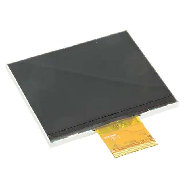


 工商网监
湘ICP备2023018690号
工商网监
湘ICP备2023018690号
