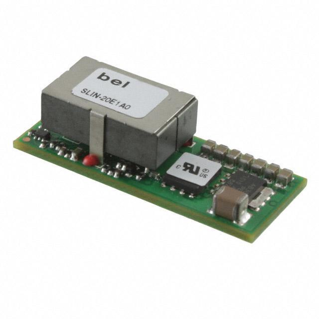
The SLIN-20F1A series of power modules are non-isolated DC/DC
converters that can deliver up to 20 A of output current. These
modules operate over a wide range of input voltage (VIN = 2.4 - 5.5
VDC) and provide a precisely regulated output voltage from 0.6 VDC
to 3.63 VDC, programmable via an external resistor.
Features include remote on/off, adjustable output voltage, over
current protection, over temperature protection and output voltage
sequencing. A new feature, the Tunable LoopTM, allows the user to
optimize the dynamic response of the converter to match the load
with reduced amount of output capacitance leading to savings on
cost and PWB area.
•
•
•
•
•
•
•
•
•
•
•
•
•
•
2.4 – 5.5 VDC Input
0.6 – 3.63 VDC / 20 A Outputs
Wide Input Voltage Range
Flexible Output Voltage Sequencing
Output Voltage Programmable
Over Temperature Protection
Fixed Switching Frequency
Output Over Current Protection
Remote On/Off
Ability to Sink and Source Current
Remote Sense
Cost Efficient Open Frame Design
Tunable LoopTM (a Registered Trademark of Lineage Power Systems) to
Optimize Dynamic Output Voltage Response
Class II, Category 2, Non-Isolated DC-DC Converter (refer to IPC9592B)
Certificated to UL/CSA 62368-1
•
•
•
•
•
•
Distributed Power Architectures
Servers and Storage Applications
Intermediate Bus Voltage Applications
Networking Equipment
Telecommunications Equipment
Industrial Equipment
•
�SLIN-20F1A
2
MODEL NUMBER
ACTIVE LOW
MODEL NUMBER
ACTIVE HIGH
SLIN-20F1ALG
SLIN-20F1A0G
SLIN-20F1ALR
SLIN-20F1A0R
-
OUTPUT
VOLTAGE
INPUT VOLTAGE
MAX. OUTPUT
CURRENT
TYPICAL
EFFICIENCY
0.6 - 3.63 VDC
2.4 - 5.5 VDC
20 A
90.8%
S
LIN
20
F
1A
x
y
Mounting
Type
Series Code
Output
Current
Input Voltage
Range
Sequencing
or not
Active Logic
Package
Surface
Mount
SLIN Series
20 A
2.4 - 5.5 V
with
Sequencing
PARAMETER
DESCRIPTION
0 – Active High
G – Tray Package
L - Active Low
R – Tape and Reel Package
MIN
TYP
Continuous Input Voltage
-0.3
Sequencing Voltage
-0.3
Operating Ambient Temperature
-40
Storage Temperature
-55
-
Altitude
MAX
UNITS
-
6
V
-
Vin,max
V
-
85
C
-
125
C
-
2000
m
NOTE: Stresses in excess of the absolute maximum ratings can cause permanent damage to the device. These are absolute stress ratings
only, functional operation of the device is not implied at these or any other conditions in excess of those given in the operations sections of
the data sheet. Exposure to absolute maximum ratings for extended periods can adversely affect the device reliability.
PARAMETER
DESCRIPTION
MIN
TYP
MAX
2.4
-
5.5
V
VIN = 2.4 V to 5.5 V, Io = Io, max
-
-
19.5
A
VIN = 5.0 V, Vo = 0.6 V, Io = 0, module enabled
-
47
-
VIN = 5.0 V, Vo = 3.3 V, Io = 0, module enabled
-
52
-
VIN = 5 V, module disabled
5 Hz to 20 MHz, 1 μH source impedance.
VIN = 0 to 5.5 V, Io = Io,max
-
5
-
mA
-
12
-
mA
Operating Input Voltage
Input Current
Input Current (no load)
Input Stand-by Current
Input Reflected Ripple Current (pk-pk)
UNIT
mA
I2t Inrush Current Transient
-
-
1
A2s
Input Ripple Rejection (120 Hz)
-
43
-
dB
Turn-on Threshold
-
2.2
-
V
Turn-off Threshold
-
2.0
-
V
0.08
-
0.2
V
Hysteresis
CAUTION: This converter is not internally fused. An input line fuse must be used in application.
This power module can be used in a wide variety of applications, ranging from simple standalone operation to an integrated part of
sophisticated power architecture. To preserve maximum flexibility, internal fusing is not included; however, to achieve maximum safety and
system protection, always use an input line fuse. The safety agencies require a fast-acting fuse with a maximum rating of 20A.
Based on the information provided in this data sheet on inrush energy and maximum dc input current, the same type of fuse with a lower
rating can be used. Refer to the fuse manufacturer’s data sheet for further information.
NOTE: Unless otherwise indicated, specifications apply over entire operating input voltage range, resistive load, and temperature conditions.
tech.support@psbel.com
�SLIN-20F1A
3
PARAMETER
DESCRIPTION
With 0.5% tolerance for external resistor used to set
output voltage
Over entire operating input voltage range, resistive load,
and temperature conditions until end of life
Output Voltage Set Point
Output Voltage
Adjustment Range
Selected by an external resistor
Remote Sense Range
MIN
TYP
MAX
UNIT
-1.5
-
+1.5
%Vo,set
-3.0
-
+3.0
%Vo,set
0.6
-
3.63
V
V
-
-
0.5
Output Regulation
(for Vo ≥ 2.5 Vdc)
Line Regulation, VIN = VIN, min to VIN, max
-
-
0.4
Load Regulation, Io = Io, min to Io, max
-
-
0.4
Output Regulation
(for Vo < 2.5 Vdc)
Line Regulation, VIN = VIN, min to VIN, max
-
-
10
Load Regulation, Io = Io, min to Io, max
-
-
10
Output Current Range
Hiccup Mode
-
-
20
A
Output DC Current Limit
Vo ≤ 250 mV, Hiccup Mode
-
200
-
%Io,max
Output Ripple and Noise (pk-pk)
-
20
35
mV
Output Ripple and Noise (rms)
5 Hz to 20 MHz BW, VIN = VIN, nom and Io = Io, min to
Io, max, Co = 0.1 μF // 10 μF ceramic capacitors
-
10
15
mV
Output Short-Circuit Current
Vo ≤ 250 mV, Hiccup Mode
-
30
-
%Io,max
-
2
-
ms
-
2
-
ms
-
-
3
%Vo,
set.
ms
Case 1: On/Off input is enabled and then input power is
applied (delay from instant at which VIN = VIN, min until
Vo = 10% of Vo, set)
Case 2: Input power is applied for at least one second and
then the On/Off input is enabled (delay from instant at
which Von/Off is enabled until Vo = 10% of Vo, set)
Vin = Vin, min to Vin, max, Io = Io, max, With or without
maximum external capacitance
Turn-On Delay and Rise Times
Output Voltage Overshoot
Output Voltage Rise Time
Output
Capacitance
Time for Vo to rise from 10% of Vo, set to 90% of Vo, set
-
5
-
ESR ≥ 1 mΩ
Without the Tunable LoopTM
0
-
200
ESR ≥ 0.15 mΩ
With the Tunable LoopTM
0
-
1000
ESR ≥ 10 mΩ
With the Tunable LoopTM
0
-
10000
%Vo,set
mV
µF
Dynamic Load Response
△V 50% ~ 75% of Max Load
△V 75% ~ 50% of Max Load
Peak Deviation
-
330
-
Settling Time
-
30
-
µs
-
420
-
mV
-
30
-
µs
Peak Deviation
di/dt = 10 A/µs, Vin = 3.3 V, Vo = 1.5 V,
Ta = 25°C, Co = 0
Settling Time
mV
NOTE: Unless otherwise indicated, specifications apply over entire operating input voltage range, resistive load, and temperature
conditions.
Asia-Pacific
+86 755 298 85888
Europe, Middle East
+353 61 49 8941
North America
+1 866 513 2839
© 2021 Bel Power Solutions & Protection
BCD.20146_AG
�SLIN-20F1A
4
PARAMETER
DESCRIPTION
Vo = 0.6 V
Vo = 1.2 V
Efficiency
Vo = 1.8 V
Vin= 3.3 VDC, Ta = 25°C
Io = Io, max, Vo = Vo, set
Vo = 2.5 V
Vo = 3.3 V
Vin = 5.0 V, when Vo = 3.3 V
MIN
TYP
MAX
-
70.0
-
-
81.9
-
-
87.3
-
-
90.8
-
-
92.9
-
UNIT
%
Switching Frequency
-
600
-
kHz
Over Temperature Protection
-
144
-
C
10
-
-
ms
-
-
100
-
-
100
Delay from VIN, min to application of voltage on
SEQ pin
Sequencing Delay time
Tracking Accuracy
Power-Up: 2 V/ms
Power-Down: 2 V/ms
Vin, min to Vin, max; Io, min to Io, max,
VSEQ < Vo
Weight
MTBF
Dimensions (L × W × H)
Calculated MTBF (Vin = 5 V, Io = 80% full load,
Ta = 40°C) Telcordia Issue 2, Method I Case 3
6.03
-
7,868,128
mV
g
hours
1.30 x 0.53 x 0.334
inch
33.02 x 13.46 x 8.50
mm
NOTE: Unless otherwise indicated, specifications apply over entire operating input voltage range, resistive load, and temperature
condition.
tech.support@psbel.com
�SLIN-20F1A
5
85
90
80
75
EFFICIENCY, (%)
EFFICIENCY, (%)
85
Vin=5.5V
70
Vin=3.3V
65
Vin=2.4V
60
Vin=5.5V
80
Vin=3.3V
Vin=2.4V
75
70
0
5
10
15
20
0
5
OUTPUT CURRENT, IO (A)
20
15
20
Figure 2. Vo = 1.2 V
95
95
90
90
EFFICIENCY, (%)
EFFICIENCY, (%))
15
OUTPUT CURRENT, IO (A)
Figure 1. Vo = 0.6 V
Vin=5.5V
85
10
Vin=3.3V
Vin=2.4V
80
75
Vin=3.3V
Vin=5.5V
85
Vin=5V
80
75
0
5
10
15
20
0
OUTPUT CURRENT, IO (A)
5
10
OUTPUT CURRENT, IO (A)
Figure 3. Vo = 1.8 V
Figure 4. Vo = 2.5 V
EFFICIENCY, (%))
100
95
Vin=4.5V
Vin=5.5V
90
Vin=5V
85
0
5
10
15
20
OUTPUT CURRENT, IO (A)
Figure 5. Vo = 3.3 V
Asia-Pacific
+86 755 298 85888
Europe, Middle East
+353 61 49 8941
North America
+1 866 513 2839
© 2021 Bel Power Solutions & Protection
BCD.20146_AG
�SLIN-20F1A
22
22
20
20
18
18
16
1m/s
(200LFM) 1.5m/s
(300LFM)
2m/s
(400LFM)
14
OUTPUT CURRENT, Io (A)
OUTPUT CURRENT, Io (A)
6
12
NC
0.5m/s
(100LFM)
10
8
16
2m/s
(400LFM)
14
1.5m/s
(300LFM)
12
10
NC
0.5m/s
(100LFM)
8
6
6
25
35
45
55
65
75
25
85
35
O
20
20
18
18
1.5m/s
(300LFM)
12
10
OUTPUT CURRENT, Io (A)
22
14
1m/s
(200LFM)
NC
0.5m/s
(100LFM)
8
65
75
85
Figure 7. Vo = 1.2 V
22
2m/s
(400LFM)
55
AMBIENT TEMPERATURE, TA C
Figure 6. Vo = 0.6 V
16
45
O
AMBIENT TEMPERATURE, TA C
OUTPUT CURRENT, Io (A)
1m/s
(200LFM)
16
2m/s
(400LFM)
14
12
1.5m/s
(300LFM)
1m/s
(200LFM)
NC
10
0.5m/s
(100LFM)
8
6
6
25
35
45
55
65
75
85
AMBIENT TEMPERATURE, TA OC
25
35
45
55
65
75
85
AMBIENT TEMPERATURE, TA OC
Figure 8. Vo = 1.8 V
Figure 9. Vo = 2.5 V
22
OUTPUT CURRENT, Io (A)
20
18
16
2m/s
(400LFM)
14
1m/s
(200LFM)
1.5m/s
(300LFM)
12
NC
10
0.5m/s
(100LFM)
8
6
25
35
45
55
65
75
85
O
AMBIENT TEMPERATURE, TA C
Figure 10. Vo = 3.3 V
tech.support@psbel.com
�7
OUTPUT VOLTAGE
VO (V) (10mV/div)
OUTPUT VOLTAGE
VO (V) (10mV/div)
SLIN-20F1A
TIME, t (1s/div)
Figure 12. Vin = 3.3 V, Vo = 1.2 V, Io = Io,max
OUTPUT VOLTAGE
VO (V) (10mV/div)
OUTPUT VOLTAGE
VO (V) (10mV/div)
Figure 11. Vin = 3.3 V, Vo = 0.6 V, Io = Io,max
TIME, t (1s/div)
TIME, t (1s/div)
Figure 14. Vin = 3.3 V, Vo = 2.5 V, Io = Io,max
OUTPUT VOLTAGE
VO (V) (10mV/div)
Figure 13. Vin = 3.3 V, Vo = 1.8 V, Io = Io,max
TIME, t (1s/div)
TIME, t (1s/div)
Figure 15. Vin = 5 V, Vo = 3.3 V, Io = Io,max
Asia-Pacific
+86 755 298 85888
Europe, Middle East
+353 61 49 8941
North America
+1 866 513 2839
© 2021 Bel Power Solutions & Protection
BCD.20146_AG
�SLIN-20F1A
OUTPUT CURRENT, OUTPUT VOLTAGE
VO (V) (500mV/div)
IO (A) (10A/div)
TIME, t (100s /div)
OUTPUT CURRENT, OUTPUT VOLTAGE
VO (V) (500mV/div)
IO (A) (10A/div)
Figure 18. Transient Response to Dynamic Load Change
from 0% 50% to 0%. Vin = 3.3 V, Vo = 1.8 V
OUTPUT CURRENT, OUTPUT VOLTAGE
VO (V) (500mV/div)
IO (A) (10A/div)
TIME, t (100s /div)
Figure 16. Transient Response to Dynamic Load Change
from 0% 50% to 0%. Vin = 3.3 V, Vo = 0.6 V
TIME, t (100s /div)
Figure 17. Transient Response to Dynamic Load Change
from 0% 50% to 0%. Vin = 3.3 V, Vo = 1.2 V
OUTPUT CURRENT, OUTPUT VOLTAGE
VO (V) (500mV/div)
IO (A) (10A/div)
OUTPUT CURRENT, OUTPUT VOLTAGE
VO (V) (500mV/div)
IO (A) (10A/div)
8
TIME, t (100s /div)
Figure 19. Transient Response to Dynamic Load Change
from 0% 50% to 0%. Vin = 5 V, Vo = 2.5 V
TIME, t (100s /div)
Figure 20. Transient Response to Dynamic Load Change
from 0% 50% to 0%. Vin = 5 V, Vo = 3.3 V
tech.support@psbel.com
�SLIN-20F1A
OUTPUT VOLTAGE
Vo (V) (200mV/div)
OUTPUT VOLTAGE
Vo (V) 500mV/div)
ON/OFF VOLTAGE
VON/OFF (V) (5V/div)
ON/OFF VOLTAGE
VON/OFF (V) (5V/div)
9
TIME, t (2 ms/div)
TIME, t (2 ms/div)
Figure 22. Start-up Using On/Off Voltage (Io = Io,max),
Vo = 1.2 V
OUTPUT VOLTAGE
Vo (V) (1V/div)
OUTPUT VOLTAGE
Vo (V) (500mV/div)
ON/OFF VOLTAGE
VON/OFF (V) (5V/div)
ON/OFF VOLTAGE
VON/OFF (V) (5V/div)
Figure 21. Start-up Using On/Off Voltage (Io = Io,max),
Vo = 0.6 V
TIME, t (2 ms/div)
Figure 24. Start-up Using On/Off Voltage (Io = Io,max),
Vo = 2.5 V
OUTPUT VOLTAGE
Vo (V) (1V/div)
ON/OFF VOLTAGE
VON/OFF (V) (5V/div)
Figure 23. Start-up Using On/Off Voltage (Io = Io,max),
Vo = 1.8 V
TIME, t (2 ms/div)
TIME, t (2 ms/div)
Figure 25. Start-up Using On/Off Voltage (Io = Io,max),
Vo = 3.3 V
Asia-Pacific
+86 755 298 85888
Europe, Middle East
+353 61 49 8941
North America
+1 866 513 2839
© 2021 Bel Power Solutions & Protection
BCD.20146_AG
�SLIN-20F1A
OUTPUT VOLTAGE
Vo(V) (500mV/div)
OUTPUT VOLTAGE
Vo(V) (200mV/div)
INPUT VOLTAGE
VIN (V) (2V/div)
INPUT VOLTAGE
VIN (V) (2V/div)
10
TIME, t (2 ms/div)
TIME, t (2 ms/div)
Figure 27. Start-up Using Input Voltage
(VIN = 3.3 V, Io = Io,max ), Vo = 1.2 V
OUTPUT VOLTAGE
Vo(V) (1V/div)
OUTPUT VOLTAGE
Vo(V) (500mV/div)
INPUT VOLTAGE
VIN (V) (2V/div)
INPUT VOLTAGE
VIN (V) (2V/div)
Figure 26. Start-up Using Input Voltage
(VIN = 3.3 V, Io = Io,max ), Vo = 0.6 V
TIME, t (2 ms/div)
Figure 29. Start-up Using Input Voltage
(VIN = 5 V, Io = Io,max ), Vo = 2.5 V
OUTPUT VOLTAGE INPUT VOLTAGE
VIN (V) (2V/div)
Vo(V) (1V/div)
Figure 28. Start-up Using Input Voltage
(VIN = 3.3 V, Io = Io,max ), Vo = 1.8 V
TIME, t (2 ms/div)
TIME, t (2 ms/div)
Figure 30. Start-up Using Input Voltage
(VIN = 5 V, Io = Io,max ), Vo = 3.3 V
tech.support@psbel.com
�SLIN-20F1A
11
Input Reflected Ripple Current Test Setup
Output Ripple and Noise Test Setup
CURRENT PROBE
TO OSCILLOSCOPE
COPPER STRIP
LTEST
RESISTIVE
LOAD
Vo+
VIN(+)
1μH
BATTERY
0.1uF
10uF
CIN
CS 1000μF
Electrolytic
COM
2x100μF
Tantalum
E.S.R.


 工商网监
湘ICP备2023018690号
工商网监
湘ICP备2023018690号
