InnoMux Family of ICs
2 Constant Voltage and 4 Channel Dimming
LED Backlight CC Controller
Product Highlights
Description
CV and 4-Channel LED Backlight Controller
When paired with InnoSwitch3-MX, InnoMux dramatically improves the
system efficiency of monitors and TVs by eliminating the boost and
buck converter stages using a single-stage flyback topology. This
enables very high system efficiency up to 91%, on a small PCB footprint.
• Eliminates buck and LED backlight boost converters
• One or two constant voltage outputs
• Independently regulated outputs with instantaneous transient
response ±5% CV on 0%-100%-0% load step
• Typical output voltages
• One CV mode: 5 V to 22 V
• Two CV mode: 5 V and 12 V to 22 V
• 1-4 string LED backlight
• 3% matching accuracy for LED strings
• Analog, PWM, sequenced PWM and filtered PWM operation
• Up to 100 V string voltage / up to 960 mA total string current
• Up to 2:1 LED string voltage range
The LED backlight control offers excellent minimum threshold regulation
as well as analog and several PWM dimming options. The sequenced
PWM dimming option further improves visual performance and stabilizes
power demand. Extensive protection features are provided.
Advanced Protection / Safety Features
• Individual overload protection for all outputs
• String imbalanced / short / open protection
• Output overvoltage set for auto-restart
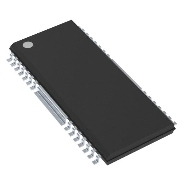
Figure 2. Left – InnoMux in QFN-28, Reflow Process.
Right – InnoMux in HSOP-28, Wave Solder Process.
InnoMux
Convenient Packages
Product
• 28-Lead HSOP for single-sided wave soldered PCBs or small 28-Lead
QFN (5x5 mm Body) for compact multilayer designs
Applications
• ENERGY STAR 8, CEC, and 2021/2023 EU labeling for monitors and
TVs
VOUT2
Package
1 CV, 1 LED string
QFN
IMX101U
1 CV, 1 LED string
HSOP
IMX111U
2 CV, 1 LED string
HSOP
IMX111J
2 CV, 1 LED string
QFN
IMX102U
1 CV, 4 LED strings
HSOP
IMX112U
2 CV, 4 LED strings
HSOP
Table 1.
VLED
Output Configuration
IMX101J
InnoMux Controller Part Numbers.
(Constant Voltage / Constant Current)
VCV2
(Constant Voltage)
VLED
VOUT1
VCV1
(Constant Voltage)
4 × LED String
VOUT
RTN
Figure 1. Typical Schematic.
ICC4
ICC3
ICC2
ICC1
IS
CTRL
PLIM2
PLIM1
VLED
FB3
VCV2
FB2
CDR2
GDR2
VCV1
FB1
CDR1
GDR1
GND
Interface with
InnoSwitch3-MX
SR
FWC
REQ
ACK
BP
BPS
PWM/APWM
ADIM/LPF
LED-EN/DPWM
Multi-Output / LED Controller
InnoMux
PI-8370-100318
www.power.com
November 2020
This Product is Covered by Patents and/or Pending Patent Applications.
�InnoMux
VCV2
VLED (CV/CC)
Up to
4 × LED String
CONTROL
Primary FET
and Controller
S
Secondary
Controller
InnoSwitch3-MX
ICC4
ICC3
ICC2
FBV1 FBV2 FBLED
ICC1
GDR2
GDR1
D
SR
FW
VCV1
PWM
ADIM/LPF
STB
Multi-Output / LED Controller
GND
InnoMux
PI-8364c-030320
Figure 3. Simplified Schematic for Monitor / TV Application.
OUTPUT VOLTAGE 3
(VCV3/VLED)
CAPACITOR 2
(CDR2)
BYPASS
(BP)
HIGH-VOLTAGE
SHUNT
ANALOG
DIMMING/
LOW PASS
FILTER
(ADIM/LPF)
CHANNEL 1 CHANNEL 2 CHANNEL 3 CHANNEL 4
(ICC4)
(ICC1)
(ICC2)
(ICC3)
CAPACITOR 1
(CDR1)
PWM
BYPASS
REGULATOR
READER
Dim
Mode
OUTPUT VOLTAGE 1
(VCV1)
HighVoltage
Clamp
HighVoltage
Clamp
HighVoltage
Clamp
HighVoltage
Clamp
ADIM
LOW VOLTAGE
SHUNT
OUTPUT VOLTAGE 2
(VCV2)
LED CONTROL
Enable
PWM DIMMING
(PWM/APWM)
LED ENABLE
(LED-EN/DPWM)
VSAT
Dim Mode
SET LED CURRENT
(IS)
FEEDBACK
(FB1)
GATE DRIVE 1
(GDR1)
FEEDBACK
(FB2)
FEEDBACK
(FB3)
HIGH-SIDE MOSFET DRIVE #1
MULTI-OUTPUT CONTROL
GATE DRIVE 2
(GDR2)
HIGH-SIDE MOSFET DRIVE #2
REQUEST
(REQ)
ACKNOWLEDGE
(ACK)
InnoSwitch3-MX
INTERFACE
POWER LIMIT1 POWER LIMIT2
(PLIM1)
(PLIM2)
SYNCHRONOUS
RECTIFIER DRIVE
(SR)
FORWARD
COMPARATOR
(FWC)
CONTROL
(CTRL)
GROUND
(GND)
PI-8328-100318
Figure 4. Functional Block Diagram of the InnoMux Controller.
2
Rev. D 11/20
www.power.com
�InnoMux
Pin Functional Description
LED-EN/DPWM
VLED
FB3
VCV2
FB2
FB1
VCV1
Leads/terminals and exposed pad
are at the bottom of the package,
shown here as hidden lines.
QFN-28 InnoMux Controller
CHANNEL 1 (ICC1) Pin (Pin 1)
LED current regulation channel 1.
CHANNEL 4 (ICC4) Pin (Pin 5)
LED current regulation channel 4.
GROUND (GND) Pin (Pin 6)
Pin 6 must be connected to the exposed pad and the secondary
ground.
SET LED CURRENT (IS) Pin (Pin 7)
Current setting for LED string current.
CONTROL (CTRL) Pin (Pin 8)
Output to control capacitor.
ANALOG DIMMING (ADIM/LPF) Pin (Pin 9)
Analog dimming/low pass filter connection.
PWM DIMMING (PWM/APWM) Pin (Pin 10)
PWM input.
SYNCHRONOUS RECTIFIER (SR) Pin (Pin 11)
SR signal from InnoSwitch3-MX.
FORWARD COMPARATOR (FWC) Pin (Pin 12)
FW comparator signal from InnoSwitch3-MX.
ACKNOWLEDGE (ACK) Pin (Pin 13)
ACK signal from InnoSwitch3-MX.
REQUEST (REQ) Pin (Pin 14)
REQ output to InnoSwitch3-MX.
POWER LIMIT 2 (PLIM2) Pin (Pin 15)
Set power limit for VLED/VCV2.
ICC1
ICC2
GND
ICC3
ICC4
GND
IS
1
2
3
4
5
6
7
QFN 28
Top View
Pad = GND
21
20
19
18
17
16
15
GDR1
CDR1
BP
CDR2
GDR2
PLIM1
PLIM2
8
9
10
11
12
13
14
CHANNEL 3 (ICC3) Pin (Pin 4)
LED current regulation channel 3.
CTRL
ADIM/LPF
PWM/APWM
SR
FWC
ACK
REQ
GROUND (GND) Pin (Pin 3)
Pin 3 must be connected to the exposed pad and the secondary
ground.
28
27
26
25
24
23
22
CHANNEL 2 (ICC2) Pin (Pin 2)
LED current regulation channel 2.
PI-8331-032019
Figure 5. InnoMux QFN-28 Controller Pin Configuration.
GATE DRIVE 1 (GDR1) Pin (Pin 21)
Selection MOSFET gate driver for CV1.
OUTPUT VOLTAGE (VCV1) Pin (Pin 22)
Output voltage connection for CV1 selection MOSFET drive.
FEEDBACK 1 (FB1) Pin (Pin 23)
Feedback input for VCV1 output voltage.
FEEDBACK 2 (FB2) Pin (Pin 24)
Feedback input for VCV2 output voltage.
POWER LIMIT 1 (PLIM1) Pin (Pin 16)
Set power limit for VCV1/VCV2.
OUTPUT VOLTAGE (VCV2) Pin (Pin 25)
Output voltage connection for BP regulator and for CV2 selection
MOSFET drive.
GATE DRIVE 2 (GDR2) Pin (Pin 17)
Selection MOSFET gate driver for CV2.
FEEDBACK 3 (FB3) Pin (Pin 26)
Feedback input for VLED output voltage.
CAPACITOR (CDR2) Pin (Pin 18)
Capacitor for GDR2.
OUTPUT VOLTAGE (VLED) Pin (Pin 27)
Output voltage connection for BP regulator.
BYPASS (BP) Pin (Pin 19)
BP/VDD regulator output. Also supplies InnoSwitch3-MX.
LED-EN/DPWM Pin (Pin 28)
LED enable/digital PWM input.
CAPACITOR (CDR1) Pin (Pin 20)
Capacitor for GDR1.
3
www.power.com
Rev. D 11/20
�InnoMux
HSOP-28 InnoMux Controller
CHANNEL 3 (ICC3) Pin (Pin 1)
LED current regulation channel 3.
CHANNEL 4 (ICC4) Pin (Pin 2)
LED current regulation channel 4.
SET LED CURRENT (IS) Pin (Pin 3)
Current setting for LED string current.
CONTROL (CTRL) Pin (Pin 4)
Output to control capacitor.
ANALOG DIMMING (ADIM/LPF) Pin (Pin 5)
Analog dimming/low pass filter connection.
PWM DIMMING (PWM/APWM) Pin (Pin 6)
PWM input.
SYNCHRONOUS RECTIFIER (SR) Pin (Pin 7)
SR signal from InnoSwitch3-MX.
ICC3
ICC4
IS
CTRL
ADIM/LPF
PWM/APWM
SR
1
2
3
4
5
6
7
GND
FWC 8
ACK 9
REQ 10
PLIM2 11
PLIM1 12
GDR2 13
CDR2 14
GROUND (GND) Pin
All grounds must connect to secondary ground.
FORWARD COMPARATOR (FWC) Pin (Pin 8)
FW comparator signal from InnoSwitch3-MX.
28
27
26
25
24
23
22
ICC2
ICC1
NC
NC
LED-EN/DPWM
VLED
FB3
GND
21
20
19
18
17
16
15
VCV2
FB2
FB1
VCV1
GDR1
CDR1
BP
PI-8330-083118
Figure 6. InnoMux HSOP-28 Controller Pin Configuration.
ACKNOWLEDGE (ACK) Pin (Pin 9)
ACK signal from InnoSwitch3-MX.
FEEDBACK 2 (FB2) Pin (Pin 20)
Feedback input for VCV2 output voltage.
REQUEST (REQ) Pin (Pin 10)
REQ output to InnoSwitch3-MX.
OUTPUT VOLTAGE (VCV2) Pin (Pin 21)
Output voltage connection for BP regulator and for CV2 selection
MOSFET drive.
POWER LIMIT 2 (PLIM2) Pin (Pin 11)
Set power limit for VLED/VCV2.
POWER LIMIT 1 (PLIM1) Pin (Pin 12)
Set power limit for VCV1/VCV2.
GATE DRIVER 2 (GDR2) Pin (Pin 13)
Selection MOSFET gate drive for CV2.
CAPACITOR (CDR2) Pin (Pin 14)
Capacitor for GDR2.
BYPASS (BP) Pin (Pin 15)
BP/VDD regulator output. Also supplies InnoSwitch3-MX.
CAPACITOR (CDR1) Pin (Pin 16)
Capacitor for GDR1.
GATE DRIVE 1 (GDR1) Pin (Pin 17)
Selection MOSFET gate drive for CV1.
OUTPUT VOLTAGE (VCV1) Pin (Pin 18)
Output voltage connection for CV1 selection MOSFET drive.
FEEDBACK 3 (FB3) Pin (Pin 22)
Feedback input for VLED output voltage.
OUTPUT VOLTAGE (VLED) Pin (Pin 23)
Output voltage connection for BP regulator.
LED-EN/DPWM Pin (Pin 24)
LED enable/digital PWM input.
NOT CONNECTED (NC) Pin (Pin 25)
This pin is not connected and should be left floating.
NOT CONNECTED (NC) Pin (Pin 26)
This pin is not connected and should be left floating.
CHANNEL 1 (ICC1) Pin (Pin 27)
LED current regulation channel 1.
CHANNEL 2 (ICC2) Pin (Pin 28)
LED current regulation channel 2.
FEEDBACK 1 (FB1) Pin (Pin 19)
Feedback input for VCV1 output voltage.
4
Rev. D 11/20
www.power.com
�InnoMux
InnoMux Functional Description
When paired with the InnoSwitch3-MX, the InnoMux combines dual
constant voltage output regulation with a four string constant current
LED backlight controller.
The InnoMux controller consists of a multi-output controller for
regulating the three outputs independently, a BP Regulator for supplying both the InnoMux as well as the paired InnoSwitch3-MX secondary controller, High-Side MOSFET Drivers for directing the energy
from the transformer to the appropriate output, Shunts to prevent
individual outputs from rising in abnormal loading conditions, Current
Sources to drive up to four LED backlight strings, and Readers to
determine the value of application configuration resistors.
Block Diagram
BP Regulator
The regulator regulates the BP pin to VBP(REG). The BP regulator will
use VCV2 as its primary source. During start-up, the regulator will use
VLED as long as VCV2 is too low (below VCV2(MIN)).
It is possible to connect an unregulated supply to VCV2 to power the
controller in single CV applications. For the controller to function
properly, the application designer must make sure that VCV2 remains
above VCV2(MIN) in all operating conditions after start-up.
A ceramic capacitor on the BP in is recommended. There are no
stability requirements on the capacitor; the BP regulator is unconditionally stable.
Multi Output Control
The multi output control regulates each of the two CV outputs and
the LED output independently by requesting pulses from the primary
based on the FB pin voltages for the three outputs. The transformer
energy is then directed to the output that needs the energy on a
cycle by cycle basis by turning on the appropriate selection MOSFET
in series with either the CV1 or the CV2 output. The transformer shall
be designed such that the VOR is increasing from VCV1 to VCV2 to
VLED, this guarantees that the current through the VLED diode is
negligible when the selection MOSFET for either VCV1 or VCV2 is
turned on; only disabling both MOSFETs will direct the energy delivery
to the LED output.
Due to the restriction in VOR, the maximum suggested LED output
voltage range is about 2:1. A larger range will yield a less optimized
design, as the VOR of the CV outputs gets very low. This is further
explained in the applications section.
The controller uses a variable frequency control scheme. The CV
outputs can run in continuous conduction mode (CCM) during high
load. The VLED output will always run discontinuous conduction mode
(DCM) to prevent high reverse recovery losses in the high voltage
silicon diode for the VLED output.
High-Side MOSFET Drive
The high side selection MOSFETs are driven with a drive voltage 5 V
above VCV1 for GDR1 and 5V above VCV2 for GDR2 using a capacitive
drive approach.
The capacitive drive approach benefits from easy level translation by
use of capacitor CDR. A regular refresh cycle to top up the charge on
CDR is needed when one of the switches has been on for a long time,
as the charge on CDR will otherwise slowly leak away. Refresh is also
needed during start-up to allow CDR to follow the output voltage when
the output is being pulled up. The controller will perform refresh
cycles when necessary by turning the selection MOSFET off and then
back on.
The default refresh time is TRESFRESH, which is doubled to 2 � TRESFRESH
during start-up. The longer the refresh time the better but the
MOSFET needs to be turned back on before the end of the primary
on time. Once the CV outputs are in regulation the refresh time is
reduced to TRESFRESH. Because the output is no longer changing the
refresh is only needed to top up CDR and by reducing the refresh time
the risk of the primary on time finishing before the refresh is reduced.
The optimal capacitor value for CDR depends on the gate charge of
the selection MOSFET. The selection MOSFET on-level gate voltage is
determined by VBP � (CDR/(CG + CDR), so it is essential that the gate
charge (at 5 V gate voltage) is much smaller than the charge in the
CDR cap. A typical value for the CDR capacitor is 100nF. For higher CDR
capacitor values, the refresh time might be insufficient and the
capacitor will not be able to follow the output during start-up. It is
therefore important to select low gate-charge devices for the
selection MOSFETs to minimise the required CDR capacitor value as
well as to minimise energy consumption for driving the MOSFETs.
Shunts
The LV shunt is designed to limit the voltage lift on the VCV1 output.
Voltage lift on the VCV1 output will typically occur due to the lower
VOR of the 5 V output. At turn-on of the 5 V selection MOSFET after
delivery of a pulse to one of the other outputs, a small amount of
energy is delivered to the CV1 output from the higher idle ring
voltage.
The LV shunt is turned on when the FB1 voltage exceeds VLVSHUNT.
In practical applications it is unlikely for the CV1 output to lift; CV1
output lift typically only occurs when the CV1 output is completely
unloaded while the other outputs are running at high output load.
The HV shunt is used to limit the voltage on the VLED rail to the
maximum allowed voltage in case of peak-charging of the VLED output
when the LED output is not loaded. This peak charging is predominantly caused by leakage in the transformer; the VLED output typically
has lowest leakage and thus will receive a small amount of energy
from switching cycles that are destined for VCV1 or VCV2.
The HV shunt is turned on when the FB3 voltage exceeds VHV(SHUNT).
In case of application problems with overvoltage on VLED, it is possible
to implement an additional Zener diode clamp with a small series
resistor to dissipate the excess power as the range between VFB3(REG)
and VFB3(OVP) is sufficiently large.
Note that the VCV2 output does not need a shunt as this output is not
susceptible to peak charging or unintended energy delivery.
5
www.power.com
Rev. D 11/20
�InnoMux
LED Current Control
InnoSwitch3-MX Interface
Operation
Current sources control the current into the ICC pins.
The InnoMux to InnoSwitch3-MX interface is a four-wire interface.
The maximum current for each current source is IICC(MAX). The desired
(full-scale) current for each of the current sources can be set by a
single external current sense resistor RLED (which is connected to the
IS pin).
The design of the current sources guarantees that the current in each
of the strings is tightly balanced.
Current sources can be paralleled (ganged together) when only one
or two strings are used. This will increase the maximum allowed
string current.
The current sources accommodate PWM dimming, analog dimming
and hybrid dimming. Hybrid dimming is a combination of analog and
PWM dimming. Dimming is further described in Led Dimming section.
Output Voltage Regulation for VLED Output
InnoMux keeps the voltage drop over the current sources as low as
possible to maintain optimum system efficiency. The output voltage
for driving the LED string(s) (VLED) is therefore regulated based on the
minimum required voltage drop over the four current sources. The
low voltage drop over the current sources is maintained for any LED
current by changing the VLED output voltage set point.
When the LEDs are on, the voltage on the CCTRL capacitor is used as
set point for the VLED output voltage. The voltage on the capacitor is
increased when the voltage drop over anyone of the current sources
is less than the target value. Vice versa, the voltage on the cap is
reduced when the voltage on all current sources is too high.
The regulation loop is subject to stability criteria and the capacitor
has to be chosen accordingly; the optimal capacitor value depends on:
The REQ signal indicates a request from the InnoMux controller for a
new pulse. Upon reception, InnoSwitch3-MX will then communicate
this request to the primary side controller over the integrated
flux-link. (Note that the InnoSwitch3-MX will delay the request to the
primary when in DCM to achieve QR mode switching.)
The REQ signal is also used to communicate timing for specific events
during start-up as well as error conditions to the InnoSwitch3-MX. For
this reason, REQ is a multi-level signal. The levels are shown in the
table below.
REQ Pin Voltage Level
REQ < 0.25 × VREF
0.25 × VREF < REQ <
0.5 × VREF
0.5 × VREF < REQ < VREF
C CTRL
$
C CTRL
$
0.3 # Gm CTRL(UP)
# FB3RATIO # C VLED
0.2 # ILED
4 # Gc CTRL(DOWN) # FB3RATIO
The first formula guarantees that the maximum dV/dt on the VLED
voltage rail is larger than the dV/dt on the CCTRL capacitor. The
second formula makes sure that the reduction in voltage on the CCTRL
capacitor is smaller than the measured voltage error on the VLED rail
Initial level at power-up.
No pulse requested by InnoMux.
InnoSwitch3-MX secondary on
stand-by / in primary control mode.
InnoSwitch3-MX secondary will start
handshake and obtain control when
the first pulse is requested.
InnoMux indicates measurement
window to InnoSwitch3-MX for idle
ring frequency measurement. This is a
one-off event during stat-up.
No pulse requested by InnoMux.
VREF < REQ < 2VREF
Pulse requested by InnoMux.
InnoMux will retain the REQ level until
the pulse request has been acknowledged (pulse on ACK pin) by InnoSwitch3-MX and a rising edge is
observed on the SR pin.
REQ > 2VREF
Output overvoltage indication by
InnoMux.
InnoSwitch3-MX secondary will signal
the primary to latch-off.
1. The ratio of the LED rail output capacitance (C VLED) to the
available current for increasing the VLED rail voltage;
2. The FB3 voltage divider ratio (FB3RATIO=VLED/VFB3).
The minimum capacitance value for the CCTRL capacitor is given by the
following formulae; both conditions have to be met:
Condition
The ACK signal indicates that a pulse request has been made by
InnoSwitch3-MX secondary to the primary controller (via the flux
link). The rising edge of the SR signal (driven by InnoSwitch3-MX) is
used byInnoMux to assess when the transformer starts delivering
energy to the secondary.
The PCB trace connecting the REQ pins deserves specific attention
during layout; it is a high-impedance multi-level analog signal and is
sensitive to noise pick-up and layout impedance.
For typical designs, 220 nF is a good starting point.
Readers
Low Current Clamps
Low-current clamps on each of the ICC outputs are designed to
prevent over voltage conditions on the ICC pins when the LEDs are
turned off. The maximum current for these clamps is ICCHV(CLAMP).
These clamps will limit the voltage on the ICC pins below VHV(CLAMP) in
LED off conditions, even when the nominal LED string voltage (VF) is
about 100 V.
The (pin-) readers determine the presence and value of the resistors/
capacitors connected to the PLIM and ADIM inputs. These readers
are active only directly after start-up and will not update until the
next power-up.
6
Rev. D 11/20
www.power.com
�InnoMux
Start-Up
LED String Configuration Detection
During start-up, the InnoSwitch3-MX will run at a fixed frequency and
50% of maximum ILIM. The InnoMux controller will first bring up VLED
to VSTAYALIVE level, a sufficient level to provide power to the BP regulator
or to 20% of the target value, whichever is highest. As soon as the
VLED has reached the designated level, the controller will start bringing
up VCV2 to 20% of the target value and finally the VCV1 to 10% of the
target value. When all three outputs are at the correct level, the
InnoMux controller will take control and bring up VCV1 and VCV2
simultaneously. The voltage on the control capacitor is slowly
increased and is used as the reference for the VCV1 and VCV2 outputs
during pull up. The size of the CCTRL capacitor will affect the rate of
rise of the outputs during pull up.
During pull up of the CV outputs, the controller will also increase the
VLED and try to run a small amount of current through the LEDs strings
to detect which of the four ICC pins have an LED string attached and
whether any of the ICC pins have been connected in parallel in a
supported configuration. Unused pins should be connected to GND
and will be disabled by the controller.
The LEDs will only be enabled after VCV1 and VCV2 have reached
regulation voltage. At this moment, the CV output regulators switch
to a fixed internal reference and the VLED output will start using the
voltage on CCTRL as its set point.
At start-up, the controller will verify that none of the connected LED
strings is short-circuit (the ICC pin connected directly to the VLED
supply rail). If one of the strings were short-circuit, the response
depends on the maximum LED voltage. For low-voltage LED
configurations (up to about 55 V maximum LED string voltage), the
affected string will be turned off and the controller will start-up as
normal. For high voltage LED configurations, the controller will
auto-restart as the short-circuit string could violate the maximum
allowed ICC pin voltage. The low-voltage / high-voltage detection is
based on the FB3 resistor ratio, which is determined at start-up.
PI-8841-100418
Figure 7 shows a schematic representation of the start-up process.
VLED
20%
VSTAYALIVE
100%
VCV2
20%
100%
VCV1
20%
10%
100%
VCTRL
20%
InnoSwitch3-MX
Wake-up
InnoMux
Takes Control
LED Detection
Complete
CV Outputs
100%
LED Enabled
InnoMux
Wake-up
Figure 7. Start-Up Diagram.
7
www.power.com
Rev. D 11/20
�InnoMux
LED Dimming
varying the voltage on the ADIM pin. The third mode is a combination of analog and PWM dimming.
The current through the LED strings can be varied for changing
(dimming) the LED brightness.
The LED dimming mode is selected at start-up and is determined by
the level on the ADIM pin. A pull-up connection / resistor to BP
selects the PWM only dimming mode. (The value of the pull-up
resistor will then select between normal and sequenced PWM. A low
signal level at start-up (ADIM voltage below VADIM(SEL)) will select the
analog or the hybrid dimming mode.
Three LED dimming modes are supported:
1. PWM only dimming with fixed output current
2. Analog dimming, output current set by an external reference
voltage (VADIM)
3. Hybrid dimming: analog dimming and PWM dimming combined.
After start-up, the dimming mode is fixed and cannot be changed
without a power-on reset.
The first dimming mode only supports PWM dimming. In this mode,
the LED current is set by a resistor on the IS pin. The analog
dimming mode (second mode) allows reducing the LED current from
100% (as set by RLED on the IS pin) to 0 (minimum current: ICC(MIN)) by
Dim Mode Select
LED_EN/DPWM
Sequenced PWM
Normal PWM
RPWM(SEL) ≤ 10 kΩ
RPWM(SEL) = 91 kΩ
High
High
High
PWM/APWM
VADIM/LPF
Figure 8 below shows an overview of the available dimming modes in
the InnoMux controller.
Analog
Hybrid Analog / PWM
Hybrid Analog / Sequenced PWM
DC Input or Filtered PWM
DC Input or Filtered PWM
DC Input or Filtered PWM
VADIM < 2.4 V at Start-up
VADIM < 2.4 V at Start-up /
Default
Low
Tied High (Low R)
Tied High (High R)
IADIM (20 µA)
Off
Off
LED Current
100%
100%
or
Driven DC Input
Off
Off
or
External RC Filter Driven DC Input
External RC Filter
or
or
or
Off
or
VADIM < 2.4 V at Start-up /
Custom Option
Off
or
Driven DC Input
Off
or
External RC Filter
or
ADIM pin (VISREF = 100%)
ADIM pin (VISREF = 100%)
ILED1
or
or
or
ILED2
or
or
or
ILED3
or
or
or
ILED4
or
or
or
DPWM pin low
DPWM pin low
DPWM pin low
DPWM pin low / 0% duty
DPWM pin low / 0% duty
DPWM pin low / 0% duty
LED Off
LED Voltage
Regulator Disabled
LED_EN pin low /
PWM pin low
LED_EN pin low /
PWM 0% duty
LED_EN pin low /
PWM pin low
LED_EN pin low /
PWM 0% duty
ADIM pin (VISREF = 100%)
PI-8842-020320
Figure 8. InnoMux Dimming Modes.
8
Rev. D 11/20
www.power.com
�InnoMux
PWM Dimming Only
IOUT is the ICC pin current (for four string operation, the total current
equals 4 × IOUT), VADIM is the voltage on the ADIM pin (1.5 V is full
scale). The result gives the resistor value for RLED which sets the
current for each of the ICC pins. As the formula is non-linear, the
desired ICC pin current must be given in Ampere (A, not mA) and the
result is in Ohms (Ω).
By connecting the ADIM/LPF pin to BP, the LED current (per string) is
set by the RLED resistor based on an internal reference (VIS(REF)).
I
RLED = VIS(REF) # b OUT l
561.56
-1.015
Figure 9 shows a graph of RLED vs. LED string current at VADIM = 1.5 V.
This graph can be used for estimating the required RLED.
The formula shows the relationship between the desired output
current and the required value for the current setting resistor.
The ADIM pin is normally driven from an external source (e.g. display
controller) to set the display brightness.
IOUT is the ICC pin current (for four string operation, the total current
equals 4 × IOUT), VIS(REF) is an internally generated reference voltage of
1.5 V. The result gives the resistor value for RLED which sets the
current for each of the ICC pins. As the formula is non-linear, the
desired ICC pin current must be given in Ampere (A, not mA) and the
result is in Ohms (Ω).
It is possible to use a PWM signal (A-PWM) to generate the analog
dimming reference (VADIM) for the LED current; the duty cycle on the
APWM pin is then accurately converted into an analog dimming
reference voltage on the ADIM/LPF pin by a simple external RC low
pass filter fed by an on chip current source providing IPWM(LPF).
Figure 9 shows a graph of RLED vs. LED string current. This graph can
be used for estimating the required RLED.
The low pass filter needs a 75 kW resistor to allow regulating up to
100%. The capacitor is typically chosen as 10 nF, but can be
changed if a different RC time constant would be desired.
PWM dimming is supported by applying a PWM signal with desired
duty cycle to the PWM pin. The allowed PWM frequency range is
PWMF(RANGE). Pulling the LED-EN pin low will turn off the LEDs as well
as the LED regulator. This is intended for disabling the LEDs during a
‘screen-off’ mode. Turning off the LED regulator will reduce chip
current consumption.
The APWM pin should be tied low when a DC voltage is supplied to
the ADIM/LPF pin.
The DPWM pin should be high during analog dimming. Pulling the
DPWM pin low will turn off the LEDs and the LED regulator. This is
intended for disabling the LEDs during use in a ‘screen-off’ mode.
Reducing the ADIM voltage down to 0 V to turn the LEDs off is not
allowed for disabling the LEDs.
Notes:
• P
ulling the PWM pin low to turn the LEDs off is allowed. Keeping
the PWM pin low longer than the minimum PWM period will also
turn off the LED regulator, independent of the LED-EN signal.
• P
ulling LED-EN low will override the state of the PWM signal.
Figure 11 (page 12) shows the typical connections in this mode for
the DPWM, APWM and analog dimming reference (VADIM) signals.
PWM dimming is supported using normal PWM dimming and
sequenced (phase shifted) PWM dimming. Normal PWM and
sequenced PWM are further explained in the section on PWM
dimming (These two PWM dimming modes are also supported in the
hybrid dimming mode, see below.)
Analog and Hybrid Dimming Modes
35
Analog Dimming
In the analog dimming mode, the voltage on the ADIM/LPF pin
determines the LED current. The LED current changes linearly over
the VADIM range. The 100% LED current level (per string) is set by the
RLED resistor.
-1.015
I
RLED = VADIM # b OUT l
561.54
30
25
20
15
10
5
0
0
50
100
150
200
250
300
String Current (mA)
The formula shows the relationship between the desired output
current and the required value for the current setting resistor.
Table 2.
PI-8998a-011020
40
RLED [kΩ]
Figure 11 (page 12) shows the typical connections in this mode for
the PWM and LED-EN signals. The RPWM(SEL) pull-up resistor selects
between normal and sequenced PWM mode.
45
Figure 9. RLED vs. LED String Current for PWM Dimming and at VADIM = 1.5 V
for Analog Dimming.
LED Configuration
Required Phase Shift
Description
1−2−3−4
0°, 90°, 180°, 270°
1−2−3
0°, 120°, 240°
1−3
0°, 180°
Two strings only. Output 3 180° phase shifted with respect to
output 1.
1 2 − 34
0°, 180°
Same as above, but now with outputs 1+2 and 3+4 ganged
together. Outputs 3 and 4 180° phase shifted with respect to
outputs 1 and 2.
Four strings. All outputs 90° phase shifted.
Three strings. Outputs 1, 2, and 3 all 120° phase shifted.
Output 4 not used.
Sequenced PWM Dimming Options.
9
www.power.com
Rev. D 11/20
�InnoMux
Hybrid Dimming
PWM dimming is supported during analog dimming by applying a
PWM signal (D-PWM) with desired duty cycle to the DPWM pin. The
allowed PWM frequency range is PWMF(RANGE). The LEDs are turned
off by pulling the DPWM pin low. Normal PWM is active by default.
Sequenced PWM is available as a custom option. (The RPWM(SEL)
resistor is not available in this mode.)
Pulling the DPWM pin low longer than the minimum PWM period will
turn off the LED regulator, which will reduce chip current consumption in a ‘screen-off’ mode. Reducing the ADIM voltage down to 0 V
to turn the LEDs off is not allowed for disabling the LEDs.
Figure 11 (page 12) shows the typical connections in this mode for
the DPWM, APWM and external LED current reference (VADIM) signals.
PWM Dimming
In PWM dimming, the LED current sources switch rapidly between the
set reference current and off, following the digital state of the PWM input.
Two PWM dimming modes are available; normal and sequenced
PWM. In PWM dimming, the ADIM/LPF pull-up resistor value selects
between normal or sequenced PWM dimming. In hybrid dimming,
the selection between normal and sequenced PWM has been preset
and cannot be changed by application components.
Normal PWM Dimming Mode
During normal PWM mode dimming, all strings will turn on and off in
phase.
Sequenced PWM Dimming Mode
In sequenced PWM mode, the on-periods of the four LED strings are
sequenced in time by applying an equal phase shift to each of the
strings. The sequenced PWM mode is designed to improve visual
performance as well as reduce transient loading on the power supply
which will reduce audible noise. Dependent on the LED configuration,
the PWM phase shift between channels should be 90°, 120° or 180°.
The allowed LED configurations for sequenced PWM diming are
shown in Table 2.
10
Rev. D 11/20
www.power.com
�InnoMux
The controller will revert to normal PWM dimming if sequenced PWM
is selected with an unsupported LED string configuration.
Typical low PWM duty cycle examples for two, three and four strings
are shown in Figure 10. It shows the relative timing of the LED
currents in two, three and four-channel sequenced PWM dimming
operation. The top waveform depicts the incoming PWM signal
(PWM/D-PWM).
Two Channel
PWM IN
PWM 1
PWM 2
PWM on-time
PWM period
Three Channel
PWM IN
PWM 1
PWM 2
PWM 3
PWM on-time
PWM period
Four Channel
PWM IN
PWM 1
PWM 2
PWM 3
PWM 4
PWM on-time
PWM period
PI-8837-100318
Figure 10. PWM Timing Diagram for Two, Three and Four Channel Sequenced
PWM Dimming.
11
www.power.com
Rev. D 11/20
�InnoMux
Connection Diagrams for the Various Dimming Options
PWM Dimming;
PWM Mode Selection: normal / sequenced PWM by a resistor
PWM/APWM
BP
At start-up, a pull-up resistor on the ADIM pin
will select PWM dimming. The output current
follows the PWM signal. The RPWM(SEL) resistor
value selects between Normal and Sequenced
PWM.
RPWM(SEL)
ADIM/LPF
IPWM(SEL)
Analog / Hybrid Dimming;
PWM optional on LED-EN / DPWM pin
At startup, an ADIM voltage below VADIM(SEL) selects
analog / hybrid dimming. The voltage on the
ADIM pin sets the LED current; varying the
ADIM voltage will allow for analog dimming.
The LED-EN / DPWM pin will turn the LEDs on
and off and can be driven with a PWM signal
for hybrid dimming.
PWM / APWM
LED-EN / DPWM
ADIM / LPF
or High
0 – 1.5 V
Analog / Hybrid Dimming with Low Pass Filter;
PWM optional on LED-EN / DPM pin
PWM / APWM
LED-EN / DPWM
or High
In analog/hybrid dimming mode, the PWM/
APWM pin can be driven with a PWM
(A−PWM) signal. This will turn the IPWM(LPF)
current source on the ADIM/LPF pin on and
off. The simple RC filter on the ADIM/LPF
(as shown) will convert the PWM duty cycle into
an accurate analog level that is then used as
the ADIM level for the analog dimming. The
LED-EN / DPWM pin will turn the LEDs on
and off and can optionally be driven with a
second PWM signal (D-PWM) for hybrid
dimming.
IPWM(LPF)
ADIM / LPF
75 kΩ
10 nF
PI-8838-020320
Figure 11. Connection Diagrams for Dimming Options.
12
Rev. D 11/20
www.power.com
�InnoMux
Protection Features and Fault Handling
Overload / Maximum Power Protection and Maximum
Power Limit
Maximum Power Protection:
Overload / Short-Circuit Protection
The CV1, CV2 and VLED outputs have a maximum power protection.
The simplest part of the protection is to detect whether the output is
more than 10% (CV outputs) or more than 1% (VLED output) below set
point. If this condition persists for more than 32 switching cycles,
then the output is assumed to be overloaded; either the output has a
short-circuit or the overall power capability of the power supply has
been exceeded and it simply cannot keep the output in regulation.
Maximum Power Limit
The short-circuit fault protection forms an overall power limit but it
would allow the full output power to be drawn from a single output
without any further protection. Therefore, the power limit function also
includes an average frequency limit that has a user selectable level.
The power limit threshold for each of the three outputs is set by the
designer using external components on the two PLIM pins. Four
setting levels for each output are available.
The power limit measures the average frequency of switching pulses
to a specific output. If this frequency is above a preset threshold for
a certain amount of time, then a fault is flagged and the controller
will auto restart or latch-off.
For calculating the maximum power limit threshold, the frequency for
a specific output should be calculated as a fraction of the maximum
total output power.
fLIMIT =
POUTPUT(MAX)
PMAX
fMAX
fLIMIT
POUTPUT^MAX h
# fMAX
PMAX
Maximum allowed power for this output
Maximum total output power
Operating frequency at maximum output power
Calculated maximum frequency for this output
The maximum overload duration is set such that the load is able to
draw at least double the nominal power for at least 10 ms, assuming
the load is not drawing more power than the power supply is
physically capable of delivering.
Table 3.
The power for CV2 is selected with the presence or absence of
capacitors on PLIM1 and PLIM2 as shown in the table below. If there
is no CV2 output then no capacitors are needed.
Table 4.
PLIM1
PLIM2
30 kHz
No Capacitor
No Capacitor
41 kHz
Capacitor
No Capacitor
56 kHz
No Capacitor
Capacitor
78 kHz
Capacitor
Capacitor
CV2 Power Limit Selection.
The time constant for the PLIM resistor and capacitor should be
chosen as TPLIM. This defines the capacitor value for a given resistor.
Further details on setting the PLIM components can be found in the
applications section.
Output OV
Any output reaching the output overvoltage (VOV) threshold will cause
a restart or latch-off of the controller. The output OV condition is
detected on the respective FB pins for the three outputs.
LED Fault Detection
During operation, the controller will continuously monitor the voltages
on the ICC pins. If a large asymmetry between the LED strings
(>VICC(OV)) is detected, the shorter string(s) will be disabled to prevent
excessive power dissipation in the controller. Any strings that go
open-circuit or short-circuit will also be disabled.
LED return short to ground will be detected by the power limit
protection, which will force a controller restart. After restart, the
affected string will be disabled.
Over-Temperature
The thermal protection circuitry continuously measures the controller
temperature. The threshold is set at TPROT. When the temperature
rises above TPROT, the InnoMux will disable the LEDs as well as the CV
outputs with hysteretic over-temperature protection; the LEDs and CV
outputs will remain disabled and the VLED rail will be maintained at
VSTAYALIVE until the temperature drops below TPROT - THYST. The
controller will restart when the temperature has dropped below this
level.
CV1 PLIM1
VLED PLIM2
30 kHz
5.1 kW
5.1 kW
If the temperature at any moment exceeds TSD, the InnoMux will send
a latch-off request to the InnoSwitch3-MX.
41 kHz
10 kW
10 kW
Fault Handling
56 kHz
22 kW
22 kW
When a fault is flagged, the controller will either auto-restart or latch-off.
78 kHz
39 kW
39 kW
In the auto-restart condition, the InnoMux will stop requesting
switching cycles. This will cause the output rails to collapse. As
there will be no further requests, the InnoSwitch3-MX primary will
take back control after a pre-defined time-out and restart.
CV1 and VLED Power Limit Selection.
In the latch-off condition, the InnoMux will send a latch-off request
to the InnoSwitch3-MX and the primary will latch-off. This condition
will persist until the mains input power is cycled.
13
www.power.com
Rev. D 11/20
�InnoMux
Absolute Maximum Ratings1,2
BP Pin Voltage.............................................................. -0.3 V to 6 V
VCV1, VCV2 Pin Voltage...................................................-0.3 V to 25 V
VCV3 / VLED Pin Voltage............................................... -0.3 V to 125 V
GDR1, GDR2 Pin Voltage..............................................-0.3 V to 30 V
ICC1, ICC2, ICC3, ICC4 Pin Voltage............................... -0.5 V to 65 V
All Other Pins.................................................................-0.3 V to 6 V
Storage Temperatue................................................-65 °C to 150 °C
Operating Junction Temperature3.......................... -40 °C to +150 °C
Notes:
1. All voltages referenced to Secondary GROUND, TA = 25 °C.
2. Maximum ratings specified may be applied one at a time without
causing permanent damage to the product. Exposure to Absolute
Maximum Ratings conditions for extended periods of time may
affect product reliability.
3. Normally limited by internal circuitry.
Thermal Resistance
Thermal Resistance: HSOP-28 Package
(qJA).................................................... 58 °C/W1
(qJA).................................................... 50 °C/W2
(qJL).................................................... 15 °C/W3
QFN-28 Package
(qJA).................................................... 69 °C/W4
(qJA).................................................... 50 °C/W5
Parameter
Symbol
Notes:
1. Single-Layer, 2 oz. Cu. 0.36 sq. in. heat sinking area.
2. Single-Layer, 2 oz. Cu. 1.0 sq. in. heat sinking area.
3. Single-Layer, 2 oz. Cu. 0.36 & 1.0 sq. in. heat sinking area.
Thermocouple attached to ground lead shoulder, near to edge of
plastic body.
4. Dual-Layer, 2 oz. Cu. 0.36 sq. in. heat sinking area (bottom layer,
connected by 9 filled vias).
5. Dual-Layer, 2 oz. Cu. 1.0 sq. in. heat sinking area (bottom layer,
connected by 9 filled vias).
Conditions
All Voltages Referenced to GROUND / 0 V
TJ = -40 °C to 125 °C
(Unless Otherwise Specified)
Min
Typ
Max
Units
4.75
5.0
5.25
V
Pin Description and Parameters
Internal voltage supply for InnoMux and
supply for InnoSwitch3-MX
BP Pin
BP Voltage Regulation
BP Current
Standby Supply Current
VBP(REG)
IBP
18
mA
BPUV
4.4
V
ISBP(STANDBY)
6
mA
VCV1 Pin (See Note B)
Input voltage for CV1 selection MOSFET drive
VCV1
VCV1 output voltage range
3
22
V
3
22
V
Input voltage for VDD regulator and for CV2
selection MOSFET drive
VCV2 Pin (See Note B)
VCV2
VCV2(MIN)
VLED Pin
Full load excludes current consumption by
InnoSwitch3-MX and selection
MOSFET Drivers
VCV2 output voltage range
Minimum VCV2 voltage
for BP regulator
Standby 25 °C
5.8
Full Load (30 mA)
8.0
V
VLED
VLED output voltage range
20
100
V
VSTAYALIVE
Minimum VLED voltage that will always be
maintained by the controller
15
V
TREFRESH
TREFRESH is doubled during start-up
See Note D
500
ns
Gate Drive Pins
Refresh Pulse Width
GDR1
The GDR1 pin drives the CV1
selection MOSFET
14
Rev. D 11/20
www.power.com
�InnoMux
Symbol
Conditions
All Voltages Referenced to GROUND / 0 V
TJ = -40 °C to 125 °C
(Unless Otherwise Specified)
GDR1 Output
Drive Voltage
VDR1
VCV1 + VBPREG (GDR1 High)
VCV1 (GDR1 Low)
GDR1 Resistance
RDR1
TJ = 125 °C
See Note C
Parameter
Min
Typ
Max
Units
30
35
W
Gate Drive Pins (cont.)
The DR2 pin drives the CV2
selection MOSFET
GDR2
GDR2 Output Drive
Voltage
VDR2
VCV2 + VBPREG (GDR2 High)
VCV2 (GDR2 Low)
VCV2+VBPREG
(high) /
VCV2 (low)
GDR2 Resistance
RDR2
TJ = 125 °C
See Note C
30
V
35
W
FB/IS Pins
FB1
FB input for VCV1 output voltage
FB1 Regulation Voltage
VFB1(REG)
VREF
LV Shunt Threshold
VLV(SHUNT)
108% of
VREF
V
20
mA
112% of
VREF
V
ICCLV(SHUNT)
FB1 Overvoltage
See Note D
17
VFB1(OVP)
FB2
FB input for VCV2 output voltage
FB2 Regulation Voltage
VFB2(REG)
VREF
V
FB2 Overvoltage
VFB2(OVP)
112% of
VREF
V
108% of
VREF
V
10
mA
120% of
VREF
V
FB3
High-Voltage
Shunt Threshold
FB input for VLED output voltage
VHV(SHUNT)
ICCHV(SHUNT)
FB3 Overvoltage
VFB3(OVP)
See Note D
8.5
15
www.power.com
Rev. D 11/20
�InnoMux
Parameter
Symbol
Conditions
All Voltages Referenced to GROUND / 0 V
TJ = -40 °C to 125 °C
(Unless Otherwise Specified)
Min
Typ
Max
Units
InnoSwitch3-MX Interface Pins
REQ
Pulse request output Should be connected to
the InnoSwitch3-MX REQ input
ACK
Acknowledge from InnoSwitch3-MX that a
request has been issued to the primary-side.
Should be connected to the InnoSwitch3-MX
ACK output
FWC
Forward comparator output from
InnoSwitch3-MX. Should be connected to the
InnoSwitch3-MX FWC output
SR
SR output from InnoSwitch3-MX. Should be
connected to the InnoSwitch3-MX SR output
LED Regulation Pins
CTRL Pin
Maximum Current
Output to CTRL capacitor
ICTRL(POS)
ICTRL(NEG)
10
µA
ICTRL(STARTUP)
0.125 ×
ICTRL
A
Regulator Gm (UP)
GmCTRL(UP)
0 V < VICC(ERROR) < 0.3 V
0.825 ×
ICTRL
A/V
Regulator (DOWN)
GcCTRL(DOWN)
-0.3 V < VICC(ERROR) < 0 V
41.25m ×
ICTRL
C/V
ICC Pins
Regulator 1-4
ICC Voltage
Protection Limit
VICC(OV)
Minimum ICC Current
ICC(MIN)
Per channel
5
mA
Maximum ICC Current
IICC(MAX)
Per channel
240
mA
ICC Channel Matching
(See Note A)
∆100 mA
100 mA Current per string, measured in
analog dimming. Equal voltage on all
ICC pins. TJ = 25 °C
±3
%
∆5 mA
5 mA Current per string, measured in analog
dimming. Equal voltage on all ICC pins.
TJ = 25 °C
±3
%
65
V
ICC Clamp Voltage
VICC(CLAMP)
Maximum ICC Clamp
Current
ICCHV(CLAMP)
8
9
60
4
V
µA
LED Control Pins
LED-EN/DPWM and
PWM/APWM Pins
PWM/APWM/DPWM
Frequency
ADIM/PWM
Selection Voltage
VIH
LED-EN/DPWM and PWM/APWM input from
system microcontroller 0 V / 5 V, 3.3 V
compliant
2.3
PWMF(RANGE)
Frequency range
100
27,000
Hz
PWMD(RANGE)
Duty cycle range is
Minimum on-time 3 ms
2
100
%
2.4
2.5
V
VIL
VADIM(SEL)
1.5
V
16
Rev. D 11/20
www.power.com
�InnoMux
Symbol
Conditions
All Voltages Referenced to GROUND / 0 V
TJ = -40 °C to 125 °C
(Unless Otherwise Specified)
VADIM
Analog dimming mode: 2% to 100%
2% brightness for VADIM = 0.03 V
100% brightness for VADIM = VIS(REF)
Note: Minimum output current level is ICC(MIN)
Current Source
IPWM(LPF)
PWM Mode
Selection Voltage
Parameter
Min
Typ
Max
Units
TJ = 25 °C
19.6
20.0
20.4
µA
VPWM(SEL)
VADIM(SEL) < VADIM < VPWM(SEL) = Normal PWM
VADIM > VPWM(SEL) = Sequenced PWM
3.8
3.9
V
IS Pin Reference
Voltage
VIS(REF)
TJ = 25 °C
1.47
1.53
V
Current Source
IPWM(SEL)
Only enabled during start-up
IS(RATIO)
IS(RATIO) = ILED/IS
ILED = 100 mA
TJ = 25 °C
IS = 156 mA
VADIM ≈ 0.72 V
LED Control Pins (cont.)
ADIM/LPF
Maximum Voltage
IS Pin Current Gain
1.50
-20
629
642
µA
655
Other Parameters
PLIM Pins
Maximum power setting for VCV1, VCV2 and VLED
PLIM Pin RC Time
Constant
TPLIM
External RC on PLIM pins
100
Reference Voltage
VREF
TJ = 25 °C
1.194
1.218
OTL Protection
TPROT
130
142
°C
OTL Hysteresis
THYST
67
°C
OTL Shut Down
TSD
150
°C
250
µs
1.242
V
NOTES:
^ IMAX - IMIN h
A. The mismatch is calculated using the following formula: D = !
# 100%
2 # I AVG
B. V_CV2 must be greater than or equal to V_CV1.
C. This parameter is derived from characterization.
D. This parameter is guaranteed by design.
17
www.power.com
Rev. D 11/20
�2X
Rev. D 11/20
0.05
0.00
0.80
0.70
2X
7
1
0.05 C
0.20
Ref.
0.05 C
A
8
28
SIDE VIEW
TOP VIEW
Pin #1 ID
(Laser Marked)
5.00
14
22
29X
2
0.08 C
15
21
B
5.00
B
Seating Plane
// 0.05 C
0.45
0.35
28X
0.50
QFN-28
15
21
14
22
8
28
3
3.40
0.10 M C A B
0.05 M C
0.25 28X
7
1
0.05 M C A B
Pin #1 ID Chamfer
PI-8949-052219
POD-QFN-28 Rev B
NOTES:
1. Dimensioning and tolerancing per
ASME Y14.5M – 1994.
2. Unilateral tolerance zone for coplanarity applies to
the exposed pad as well as the terminals.
3. Terminal width dimension apples to the metallized
terminal and is measured between 0.15 and 0.25 mm from
the terminal tip.
4. Dimensions in millimeters.
BOTTOM VIEW
3.40
0.05 M C A B
InnoMux
18
www.power.com
�www.power.com
Pin #1 I.D.
0.80
1
28
2.35
2.25
Body Thickness
2.70 Max.
Total Mounting Height
B
7.50
2
2X
0.10 C B
A
2
5.15 Ref.
21
8
TOP VIEW
6.40 Ref.
SIDE VIEW
7
22
18.00
3
(28X)
4
C
Seating
Plane
15 Lead Tips
0.20 C
10.10
0.20 C
15 Lead Tips
Coplanarity: 30 Leads
0.10 C
0.25 M C A B
0.41
0.33
14
15
2X
0.10 C A
HSOP-28
0.85
0.55
DETAIL A
0.20
0.05
C
Seating Plane
H
Detail A
END VIEW
1.30 Ref.
0.29
0.25
3
(30X)
6. Datums A & B to be determined at Datum H.
5. Dimensions in millimeters.
4. Does not include inter-lead flash or protrusions.
3. Dimensions noted are inclusive of plating thickness.
PI-8799-082718
POD-HSOP-28 Rev A
2. Dimensions noted are determined at the outermost extremes of the
plastic body exculsive of mold flash, tie bar burrs, gate burrs, and interlead flash,
but including any mismatch between the top and bottom of the plastic body.
Maximum mold protrusion is 0.18 mm per side.
Notes:
1. Dimensioning and Tolerancing per ASME Y14.5M – 1994.
0° – 8°
Gauge
Plane
0.25
1.07
0.97
InnoMux
Rev. D 11/20
19
�InnoMux
PACKAGE MARKING
QFN-28
A
1926
IMX101J
01E8L859A
H01
B
C
D
E
A.
B.
C.
D.
E.
Power Integrations Registered Trademark
Assembly Date Code (last two digits of year followed by 2-digit work week)
Product Identification (Part #/Package Type)
Lot Identification Code
Extended Lot Identification Code
PI-9106-011020
20
Rev. D 11/20
www.power.com
�InnoMux
PACKAGE MARKING
HSOP-28
1928
IMX101U
028P002D
H01
A
A.
B.
C.
D.
E.
B
C
D
E
Power Integrations Registered Trademark
Assembly Date Code (last two digits of year followed by 2-digit work week)
Product Identification (Part #/Package Type)
Lot Identification Code
Extended Lot Identification Code
PI-9105-011020
Part Ordering Information
• InnoMux Product Family
• Series Number
• Package Identifier
U
HSOP
J
QFN
• Tape & Reel and Other Options
IMX 101 U - TL
TL
Tape & Reel, 1 k pcs per reel for HSOP, 2 k pcs per reel for QFN.
21
www.power.com
Rev. D 11/20
�Revision Notes
Date
B
Code L release.
03/19
C
Code A release.
03/20
D
Added Storage Temperature data to Absolute Maximum Rating table.
11/20
For the latest updates, visit our website: www.power.com
Power Integrations reserves the right to make changes to its products at any time to improve reliability or manufacturability. Power Integrations
does not assume any liability arising from the use of any device or circuit described herein. POWER INTEGRATIONS MAKES NO WARRANTY
HEREIN AND SPECIFICALLY DISCLAIMS ALL WARRANTIES INCLUDING, WITHOUT LIMITATION, THE IMPLIED WARRANTIES OF MERCHANTABILITY,
FITNESS FOR A PARTICULAR PURPOSE, AND NON-INFRINGEMENT OF THIRD PARTY RIGHTS.
Patent Information
The products and applications illustrated herein (including transformer construction and circuits external to the products) may be covered by one
or more U.S. and foreign patents, or potentially by pending U.S. and foreign patent applications assigned to Power Integrations. A complete list of
Power Integrations patents may be found at www.power.com. Power Integrations grants its customers a license under certain patent rights as set
forth at www.power.com/ip.htm.
Life Support Policy
POWER INTEGRATIONS PRODUCTS ARE NOT AUTHORIZED FOR USE AS CRITICAL COMPONENTS IN LIFE SUPPORT DEVICES OR SYSTEMS
WITHOUT THE EXPRESS WRITTEN APPROVAL OF THE PRESIDENT OF POWER INTEGRATIONS. As used herein:
1. A Life support device or system is one which, (i) is intended for surgical implant into the body, or (ii) supports or sustains life, and (iii) whose
failure to perform, when properly used in accordance with instructions for use, can be reasonably expected to result in significant injury or
death to the user.
2. A critical component is any component of a life support device or system whose failure to perform can be reasonably expected to cause the
failure of the life support device or system, or to affect its safety or effectiveness.
Power Integrations, the Power Integrations logo, CAPZero, ChiPhy, CHY, DPA-Switch, EcoSmart, E-Shield, eSIP, eSOP, HiperPLC, HiperPFS,
HiperTFS, InnoSwitch, Innovation in Power Conversion, InSOP, LinkSwitch, LinkZero, LYTSwitch, SENZero, TinySwitch, TOPSwitch, PI, PI Expert,
PowiGaN, SCALE, SCALE-1, SCALE-2, SCALE-3 and SCALE-iDriver, are trademarks of Power Integrations, Inc. Other trademarks are property of
their respective companies. ©2020, Power Integrations, Inc.
Power Integrations Worldwide Sales Support Locations
World Headquarters
5245 Hellyer Avenue
San Jose, CA 95138, USA
Main: +1-408-414-9200
Customer Service:
Worldwide: +1-65-635-64480
Americas: +1-408-414-9621
e-mail: usasales@power.com
China (Shanghai)
Rm 2410, Charity Plaza, No. 88
North Caoxi Road
Shanghai, PRC 200030
Phone: +86-21-6354-6323
e-mail: chinasales@power.com
Germany (AC-DC/LED Sales)
Einsteinring 24
85609 Dornach/Aschheim
Germany
Tel: +49-89-5527-39100
e-mail: eurosales@power.com
Germany (Gate Driver Sales)
HellwegForum 1
59469 Ense
Germany
Tel: +49-2938-64-39990
e-mail: igbt-driver.sales@power.com
India
#1, 14th Main Road
China (Shenzhen)
Vasanthanagar
17/F, Hivac Building, No. 2, Keji Nan Bangalore-560052 India
8th Road, Nanshan District,
Phone: +91-80-4113-8020
Shenzhen, China, 518057
e-mail: indiasales@power.com
Phone: +86-755-8672-8689
e-mail: chinasales@power.com
Italy
Via Milanese 20, 3rd. Fl.
20099 Sesto San Giovanni (MI) Italy
Phone: +39-024-550-8701
e-mail: eurosales@power.com
Japan
Yusen Shin-Yokohama 1-chome Bldg.
1-7-9, Shin-Yokohama, Kohoku-ku
Yokohama-shi,
Kanagawa 222-0033 Japan
Phone: +81-45-471-1021
e-mail: japansales@power.com
Korea
RM 602, 6FL
Korea City Air Terminal B/D, 159-6
Samsung-Dong, Kangnam-Gu,
Seoul, 135-728, Korea
Phone: +82-2-2016-6610
e-mail: koreasales@power.com
Singapore
51 Newton Road
#19-01/05 Goldhill Plaza
Singapore, 308900
Phone: +65-6358-2160
e-mail: singaporesales@power.com
Taiwan
5F, No. 318, Nei Hu Rd., Sec. 1
Nei Hu Dist.
Taipei 11493, Taiwan R.O.C.
Phone: +886-2-2659-4570
e-mail: taiwansales@power.com
UK
Building 5, Suite 21
The Westbrook Centre
Milton Road
Cambridge
CB4 1YG
Phone: +44 (0) 7823-557484
e-mail: eurosales@power.com
�


 工商网监
湘ICP备2023018690号
工商网监
湘ICP备2023018690号
