Reference
Design
Sample &
Buy
Design
Tools
®
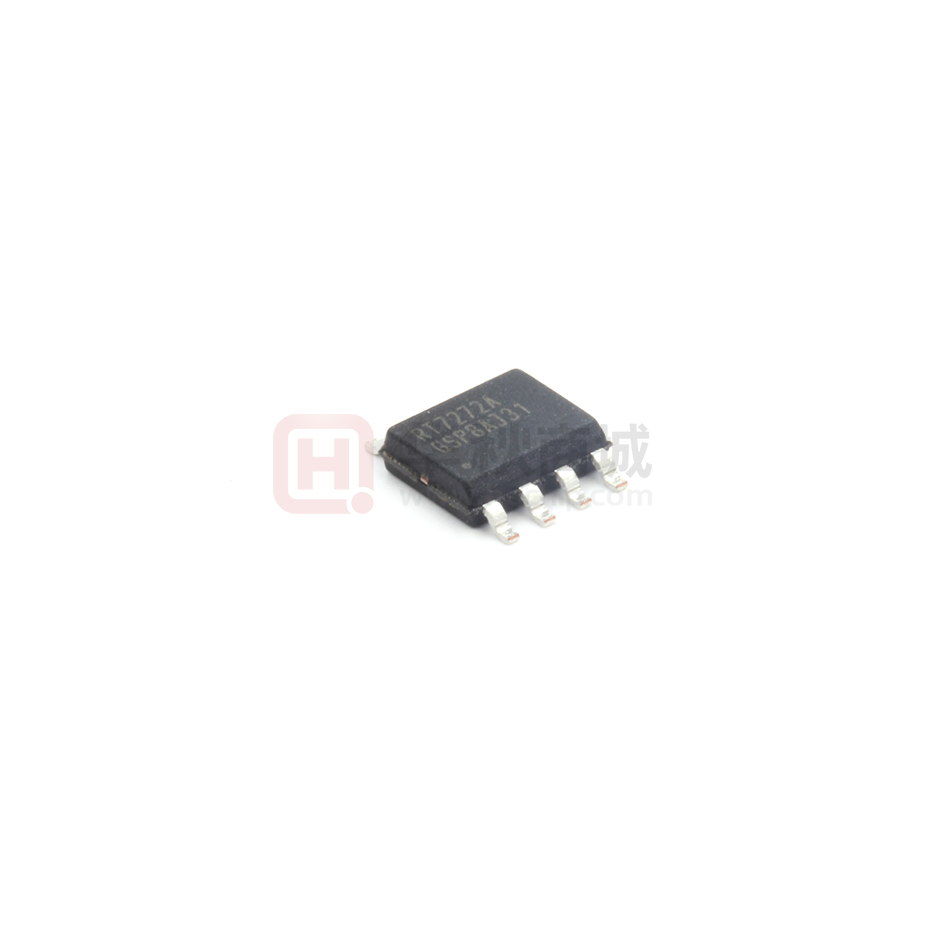
RT7272A
3A, 36V, 500kHz Synchronous Step-Down Converter
General Description
Features
The RT7272A is a high efficiency, current mode
synchronous step-down DC-DC converter that can deliver
up to 3A output current over a wide input voltage range
from 4.5V to 36V. The device integrates a 150mΩ high
side and a 80mΩ low side MOSFET to achieve high
conversion efficiency up to 95%. The current mode control
architecture supports fast transient response and simple
compensation circuit.
z
z
z
z
z
z
z
z
z
A cycle-by-cycle current limit function provides protection
against shorted output and an internal soft-start eliminates
input current surge during start-up. The RT7272A provides
complete protection functions such as input under-voltage
lockout, output under-voltage protection, over-current
protection and thermal shutdown.
z
z
z
z
z
The RT7272A is available in the thermal enhanced SOP-8
(Exposed Pad) package.
Applications
z
z
Ordering Information
z
RT7272A
z
Package Type
SP : SOP-8 (Exposed Pad-Option 2)
z
z
Lead Plating System
G : Green (Halogen Free and Pb Free)
z
Note :
z
Richtek products are :
z
`
4.5V to 36V Input Voltage Range
3A Output Current
Internal N-MOSFETs
Current Mode Control
Fixed Frequency Operation : 500kHz
Adjustable Output Voltage from 0.8V to 30V
High Efficiency Up to 95%
Stable with Low ESR Ceramic Output Capacitors
Cycle-by-Cycle Current Limit
Input Under Voltage Lockout
Output Under-Voltage Protection
Thermal Shutdown Protection
Adjustable Current Limit
RoHS Compliant and Halogen Free
Distributed Power Systems
Pre-Regulator for Linear Regulators
Notebook Computers
Point of Load Regulator in Distributed Power System
Digital Set-Top Boxes
Personal Digital Recorders
Broadband Communications
Flat Panel TVs and Monitors
Vehicle Electronics
RoHS compliant and compatible with the current requirements of IPC/JEDEC J-STD-020.
`
Suitable for use in SnPb or Pb-free soldering processes.
Simplified Application Circuit
VIN
BOOT
VIN
CIN
RT7272A
CB
L
SW
Enable
RLIM
R1
COUT
FB
CC R
C
RL
GND
Copyright © 2018 Richtek Technology Corporation. All rights reserved.
DS7272A-09 February 2018
VOUT
EN
R2
COMP
is a registered trademark of Richtek Technology Corporation.
www.richtek.com
1
�RT7272A
Marking Information
Pin Configuration
(TOP VIEW)
RT7272AGSP : Product Number
8
SW
BOOT
2
EN
3
GND
4
GND
RT7272A
GSPYMDNN
VIN
7
RLIM
6
COMP
5
FB
9
YMDNN : Date Code
SOP-8 (Exposed Pad)
Functional Pin Description
Pin No.
Pin Name
Pin Function
1
SW
Switch node. Connect to external L-C filter.
2
BOOT
Bootstrap supply for high-side gate drive. A 100nF or greater capacitor is
recommended to connect from BOOT pin to SW pin.
3
EN
Enable control input. A logic-high enables the converter; a logic-low forces the
device into shutdown mode.
4,
9 (Exposed Pad)
Ground. The exposed pad must be soldered to a large PCB and connected to
GND for maximum thermal dissipation.
Feedback input. This pin is connected to the converter output. It is used to set
the output of the converter to regulate to the desired value via an resistive
divider.
Compensation node. COMP is used to compensate the regulation control loop.
Connect a series RC network from COMP to GND. In some cases, an additional
capacitor from COMP to GND is required.
GND
5
FB
6
COMP
7
RLIM
Current limit setting. Connect to a resistor to determine current limit.
8
VIN
Power input. The input voltage range is from 4.5V to 36V. Must bypass with a
suitable large ceramic capacitor.
Functional Block Diagram
VIN
VCC
Internal
Regulator
Oscillator
Shutdown
VA VCC
Comparator
1.2V
5kΩ
RSENSE VA
0.4V
+
UV
UV
Comparator
Lockout
Comparator
-
EN
Slope Comp
Foldback
Control
+
Current Sense
Amplifier
+
-
BOOT
Q
150mΩ
R
Q
80mΩ
SW
+
Current
Comparator
+
S
GND
VCC
0.8V
SS
RLIM
+
+EA
-
FB
Copyright © 2018 Richtek Technology Corporation. All rights reserved.
www.richtek.com
2
COMP
is a registered trademark of Richtek Technology Corporation.
DS7272A-09 February 2018
�RT7272A
Operation
The RT7272A is a constant frequency, current mode
synchronous step-down converter. In normal operation,
the high side N-MOSFET is turned on when the S-R latch
is set by the oscillator and is turned off when the current
comparator resets the S-R latch. While the high side
N-MOSFET is turned off, the low side N-MOSFET is turned
on to conduct the inductor current until next cycle begins.
Current Setting
The current limit of high side MOSFET is adjustable by
an external resistor connected to the RLIM pin. The current
limit range is from 1.9A to 7A. When the inductor current
reaches the current limit threshold, the COMP voltage
will be clamped to limit the inductor current.
UV Comparator
Error Amplifier
The error amplifier adjusts its output voltage by comparing
the feedback signal (VFB) with the internal 0.8V reference.
When the load current increases, it causes a drop in the
feedback voltage relative to the reference. The error
amplifier's output voltage then rises to allow higher inductor
current to match the load current.
Oscillator
The internal oscillator runs at fixed frequency 500kHz. In
short circuit condition, the frequency is reduced to 75kHz
for low power consumption.
If the feedback voltage (VFB) is lower than 0.4V, the UV
Comparator will go high to turn off the high side MOSFET.
The output under voltage protection is designed to operate
in Hiccup mode. When the UV condition is removed, the
converter will resume switching.
Thermal Shutdown
The over temperature protection function will shut down
the switching operation when the junction temperature
exceeds 150°C. Once the junction temperature cools
down by approximately 20°C, the converter will
automatically resume switching.
Internal Regulator
The regulator provides low voltage power to supply the
internal control circuits and the bootstrap power for high
side gate driver.
Soft-Start (SS)
An internal current source charges an internal capacitor
to build a soft-start ramp voltage. The FB voltage will track
the internal ramp voltage during soft-start interval. The
typical soft-start time is 2ms.
Copyright © 2018 Richtek Technology Corporation. All rights reserved.
DS7272A-09 February 2018
is a registered trademark of Richtek Technology Corporation.
www.richtek.com
3
�RT7272A
Absolute Maximum Ratings
(Note 1)
Supply Input Voltage, VIN ----------------------------------------------------------------------------------------------Switch Voltage, SW -----------------------------------------------------------------------------------------------------SW (t < 10ns) -------------------------------------------------------------------------------------------------------------z VBOOT − VSW ---------------------------------------------------------------------------------------------------------------z Other Pins Voltage -------------------------------------------------------------------------------------------------------z Power Dissipation, PD @ TA = 25°C
SOP-8 (Exposed Pad) --------------------------------------------------------------------------------------------------z Package Thermal Resistance (Note 2)
SOP-8 (Exposed Pad), θJA ---------------------------------------------------------------------------------------------SOP-8 (Exposed Pad), θJC --------------------------------------------------------------------------------------------z Lead Temperature (Soldering, 10 sec.) ------------------------------------------------------------------------------z Junction Temperature ----------------------------------------------------------------------------------------------------z Storage Temperature Range -------------------------------------------------------------------------------------------z ESD Susceptibility (Note 3)
HBM (Human Body Model) ---------------------------------------------------------------------------------------------z
z
Recommended Operating Conditions
z
z
z
−0.3V to 40V
−0.3V to 40.3V
−5V to 46V
−0.3V to 6V
−0.3V to 40V
2.041W
49°C/W
15°C/W
260°C
150°C
−65°C to 150°C
2kV
(Note 4)
Supply Input Voltage, VIN ----------------------------------------------------------------------------------------------- 4.5V to 36V
Junction Temperature Range -------------------------------------------------------------------------------------------- −40°C to 125°C
Ambient Temperature Range -------------------------------------------------------------------------------------------- −40°C to 85°C
Electrical Characteristics
(VIN = 12V, CIN = 20µF, TA = 25°C, unless otherwise specified)
Parameter
Symbol
Shutdown Supply Current
Test Conditions
Min
Typ
Max
Unit
VEN = 0V
--
0.5
3
µA
--
0.9
1.2
mA
0.788
0.8
0.812
V
Quiescent Current
IQ
VEN = 3V, VFB = 0.9V
Feedback Reference
Voltage
VREF
4.5V ≤ VIN ≤ 36V
High Side Switch
On-Resistance
RDS(ON)1
--
150
--
mΩ
Low Side Switch
On-Resistance
RDS(ON)2
--
80
--
mΩ
--
0
10
µA
1.9
--
7
A
Min. duty cycle, RLIM = 57.6kΩ
1.9
2.5
3.1
Min. duty cycle, RLIM = 84.5kΩ
2.7
3.5
4.2
Min. duty cycle, RLIM = 137kΩ
4.8
5.5
6.3
--
1.5
--
High Side Switch Leakage
Current
VEN = 0V, VSW = 0V
Upper Switch Current Limit
Range
UOC
Upper Switch Current Limit
UOC
(Note 5)
Lower Switch Current Limit
From drain to source
Copyright © 2018 Richtek Technology Corporation. All rights reserved.
www.richtek.com
4
A
A
is a registered trademark of Richtek Technology Corporation.
DS7272A-09 February 2018
�RT7272A
Parameter
Symbol
Test Conditions
Min
Typ
Max
Unit
450
500
550
kHz
Oscillation Frequency
fOSC1
Short Circuit Oscillation
Frequency
fOSC2
VFB = 0V
--
75
--
kHz
Maximum Duty Cycle
DMAX
VFB = 0.7V
--
90
--
%
Minimum On-Time
tON_MIN
--
100
--
ns
EN Input Voltage
Logic-High
VIH
1.4
1.65
2
Logic-Low
VIL
1.2
1.45
1.9
--
0.2
--
V
3.9
4.1
4.3
V
V
EN Input Voltage Logic-High
Hysteresis
∆VIH
Input Under Voltage Lockout
Threshold
VUVLO
Input Under Voltage Lockout
Hysteresis
∆VUVLO
--
250
--
mV
Thermal Shutdown
TSD
--
150
--
°C
Thermal Shutdown Hysteresis
∆TSD
--
20
--
°C
COMP to Current Sense
Transconductance
GCS
--
4.7
--
A/V
GEA
--
1000
Load Regulation
∆VLOAD
--
Line Regulation
∆VLINE
--
VIN rising
∆ICOMP = ±10µA
Error Amplifier
Transconductance
VIN = 4.5V to 36V
--
µA/V
--
0.05
%/A
--
0.1
%
Note 1. Stresses beyond those listed “Absolute Maximum Ratings” may cause permanent damage to the device. These are
stress ratings only, and functional operation of the device at these or any other conditions beyond those indicated in
the operational sections of the specifications is not implied. Exposure to absolute maximum rating conditions may
affect device reliability.
Note 2. θJA is measured at TA = 25°C on a high effective thermal conductivity four-layer test board per JEDEC 51-7. θJC is
measured at the exposed pad of the package.
Note 3. Devices are ESD sensitive. Handling precaution is recommended.
Note 4. The device is not guaranteed to function outside its operating conditions.
Note 5. RLIM (kΩ) = [UOC x 24.14 x (1 + 0.024 x (UOC − 3.5)) − 1.3], where UOC is desired upper switch peak current limit
value.
Copyright © 2018 Richtek Technology Corporation. All rights reserved.
DS7272A-09 February 2018
is a registered trademark of Richtek Technology Corporation.
www.richtek.com
5
�RT7272A
Typical Application Circuit
VIN
4.5V to 36V
CIN
10µF x 2
Enable
8 VIN
RT7272A
2
BOOT
3 EN
SW 1
RL
137k
4, 9 (Exposed Pad)
GND
L
VOUT
R1
7 RLIM
RLIM
CB
100nF
FB 5
COMP
6
COUT
CC
RC
R2
Table 1. Suggested Component Values
VOUT (V)
R1 (kΩ)
R2 (kΩ)
RC (kΩ)
L (µH)
CC (nF)
COUT (µF)
12
47
3.35
47
10
2.7
22 x 2
8
27
3
36
8.2
2.7
22 x 2
5
62
11.8
24
6.8
2.7
22 x 2
3.3
75
24
16
4.7
2.7
22 x 2
2.5
25.5
12
12
3.6
2.7
22 x 2
1.2
30
60
6.8
2.2
2.7
22 x 2
Note : All the input and output capacitors are the suggested values, referring to the effective capacitances, subject to any derating effect, like a DC bias.
Copyright © 2018 Richtek Technology Corporation. All rights reserved.
www.richtek.com
6
is a registered trademark of Richtek Technology Corporation.
DS7272A-09 February 2018
�RT7272A
Typical Operating Characteristics
Efficiency vs. Output Current
Reference Voltage vs. Input Voltage
100
0.810
90
Efficiency (%)
VIN =
VIN =
VIN =
VIN =
70
60
Reference Voltage (V)
0.808
80
4.5V
12V
24V
36V
50
40
30
20
0.805
0.803
0.800
0.798
0.795
0.793
10
VOUT = 3.3V
VIN = 4.5V to 36V, IOUT = 0A
0
0.790
0
0.5
1
1.5
2
2.5
3
2
6.75
11.5 16.25
Output Current (A)
25.75 30.5 35.25
40
Input Voltage (V)
Reference Voltage vs. Temperature
Output Voltage vs. Output Current
3.320
0.810
3.315
0.805
Output Voltage (V)
Reference Voltage (V)
21
0.800
VIN =
VIN =
VIN =
VIN =
0.795
4.5V
12V
24V
36V
3.310
VIN = 12V
VIN = 24V
VIN = 30V
3.305
3.300
3.295
VOUT = 3.3V, IOUT = 0A
0.790
VOUT = 3.3V
3.290
-50
-25
0
25
50
75
100
0
125
0.5
1
Temperature (°C)
Switching Frequency vs. Input Voltage
2
2.5
3
Switching Frequency vs. Temperature
500
500
Switching Frequency (kHz)1
Switching Frequency (kHz)1
1.5
Output Current (A)
490
480
470
460
490
480
470
460
VIN =
VIN =
VIN =
VIN =
450
VOUT = 3.3V, IOUT = 0A
450
36V
24V
12V
4.5V
VOUT = 3.3V, IOUT = 0A
440
4
8
12
16
20
24
28
32
Input Voltage (V)
Copyright © 2018 Richtek Technology Corporation. All rights reserved.
DS7272A-09 February 2018
36
-50
-25
0
25
50
75
100
125
Temperature (°C)
is a registered trademark of Richtek Technology Corporation.
www.richtek.com
7
�RT7272A
Current Limit vs. Temperature
Load Transient Response
8
Current Limit (A)
7
VOUT
(200mV/Div)
6
5
4
IOUT
(2A/Div)
3
VIN = 12V
VIN = 12V, VOUT = 3.3V, IOUT = 1.5A to 3A
2
-50
-25
0
25
50
75
100
Time (100µs/Div)
125
Temperature (°C)
Load Transient Response
Switching
VOUT
(5mV/Div)
VOUT
(200mV/Div)
VSW
(5V/Div)
IOUT
(2A/Div)
VIN = 12V, VOUT = 3.3V, IOUT = 0 to 3A
IL
(2A/Div)
Time (100µs/Div)
Time (1µs/Div)
Power On from EN
Power Off from EN
VEN
(5V/Div)
VIN
(5V/Div)
VOUT
(2V/Div)
VOUT
(2V/Div)
IOUT
(2A/Div)
IOUT
(2A/Div)
VIN = 12V, VOUT = 3.3V, IOUT = 3A
Time (2.5ms/Div)
Copyright © 2018 Richtek Technology Corporation. All rights reserved.
www.richtek.com
8
VIN = 12V, VOUT = 3.3V, IOUT = 3A
VIN = 12V, VOUT = 3.3V, IOUT = 3A
Time (2.5ms/Div)
is a registered trademark of Richtek Technology Corporation.
DS7272A-09 February 2018
�RT7272A
Application Information
Output Voltage Setting
Chip Enable Operation
The resistive divider allows the FB pin to sense the output
voltage as shown in Figure 1.
The EN pin is a device enable input. Pulling the EN pin to
logic low that is typically less than the set threshold
voltage 1.45V, the device shuts down and enters to low
quiescent current state about 3µA. The regulator starts
switching again once the EN pin voltage exceeds the
threshold voltage 1.65V. For external timing control, the
EN pin can also be externally pulled high by adding a REN
resistor and CEN capacitor from the VIN pin (see Figure 3).
VOUT
R1
FB
RT7272A
R2
GND
EN
Figure 1. Output Voltage Setting
VIN
The output voltage is set by an external resistive voltage
divider according to the following equation :
VOUT = VREF 1+ R1
R2
Where VREF is the reference voltage (0.8V typ.).
External Bootstrap Diode
Connect a 0.1µF low ESR ceramic capacitor between the
BOOT and SW pins. This capacitor provides the gate driver
voltage for the high side MOSFET.
It is recommended to add an external bootstrap diode
between an external 5V and BOOT pin for efficiency
improvement when input voltage is lower than 5.5V or duty
ratio is higher than 65% .The bootstrap diode can be a
low cost one such as IN4148 or BAT54. The external 5V
can be a 5V fixed input from system or a 5V output of the
RT7272A. Note that the external boot voltage must be
lower than 5.5V
5V
REN
EN
RT7272A
CEN
GND
Figure 3. Enable Timing Control
An external MOSFET can be added to implement digital
control on the EN pin when no system voltage above 2.5V
is available, as shown in Figure 4. In this case, a 100kΩ
pull-up resistor, REN, is connected between VIN and the
EN pin. MOSFET Q1 will be under logic control to pull
down the EN pin.
VIN
EN
REN
100k
EN
Q1
RT7272A
GND
Figure 4. Digital Enable Control Circuit
Under-Voltage Protection
Hiccup Mode
BOOT
RT7272A
100nF
SW
Figure 2. External Bootstrap Diode
Copyright © 2018 Richtek Technology Corporation. All rights reserved.
DS7272A-09 February 2018
The RT7272A provides Hiccup Mode Under-Voltage
Protection (UVP). When the VFB voltage drops below 0.4V,
the UVP function will be triggered to shut down switching
operation. If the UVP condition remains for a period, the
RT7272A will retry automatically. When the UVP condition
is removed, the converter will resume operation. The UVP
is disabled during soft-start period.
is a registered trademark of Richtek Technology Corporation.
www.richtek.com
9
�RT7272A
Hiccup Mode
The inductor's current rating (caused a 40°C temperature
rising from 25°C ambient) should be greater than the
maximum load current and its saturation current should
be greater than the short circuit peak current limit. Please
see Table 2 for the inductor selection reference.
VOUT
(2V/Div)
Table 2. Suggested Inductors for Typical
Application Circuit
IL
(2A/Div)
IOUT = Short
Time (50ms/Div)
Figure 5. Hiccup Mode Under Voltage Protection
Over-Temperature Protection
The RT7272A features an Over-Temperature Protection
(OTP) circuitry to prevent from overheating due to
excessive power dissipation. The OTP will shut down
switching operation when junction temperature exceeds
150°C. Once the junction temperature cools down by
approximately 20°C, the converter will resume operation.
To maintain continuous operation, the maximum junction
temperature should be lower than 125°C.
Inductor Selection
The inductor value and operating frequency determine the
ripple current according to a specific input and output
voltage. The ripple current ∆IL increases with higher VIN
and decreases with higher inductance.
V
V
∆IL = OUT × 1− OUT
VIN
f ×L
Having a lower ripple current reduces not only the ESR
losses in the output capacitors but also the output voltage
ripple. High frequency with small ripple current can achieve
the highest efficiency operation. However, it requires a
large inductor to achieve this goal.
For the ripple current selection, the value of ∆IL = 0.24(IMAX)
will be a reasonable starting point. The largest ripple
current occurs at the highest VIN. To guarantee that the
ripple current stays below the specified maximum, the
inductor value should be chosen according to the following
equation :
VOUT
VOUT
L =
× 1 − VIN(MAX)
f
0.24
I
×
×
(MAX)
Copyright © 2018 Richtek Technology Corporation. All rights reserved.
www.richtek.com
10
Component
Supplier
Series
Dimensions
(mm)
TDK
VLF10045
10 x 9.7 x 4.5
TDK
TAIYO
YUDEN
SLF12565
12.5 x 12.5 x 6.5
NR8040
8x8x4
CIN and COUT Selection
The input capacitance, C IN, is needed to filter the
trapezoidal current at the Source of the high side MOSFET.
To prevent large ripple current, a low ESR input capacitor
sized for the maximum RMS current should be used. The
approximate RMS current equation is given :
V
IRMS = IOUT(MAX) OUT
VIN
VIN
−1
VOUT
This formula has a maximum at VIN = 2VOUT, where
IRMS = I OUT / 2. This simple worst case condition is
commonly used for design because even significant
deviations do not offer much relief.
Choose a capacitor rated at a higher temperature than
required. Several capacitors may also be paralleled to
meet size or height requirements in the design.
For the input capacitor, two 10µF low ESR ceramic
capacitors are suggested. For the suggested capacitor,
please refer to Table 3 for more details.
The selection of COUT is determined by the required ESR
to minimize voltage ripple.
Moreover, the amount of bulk capacitance is also a key
for COUT selection to ensure that the control loop is stable.
Loop stability can be checked by viewing the load transient
response as described in a later section.
The output ripple, ∆VOUT , is determined by :
1
∆VOUT ≤ ∆IL ESR +
8fCOUT
is a registered trademark of Richtek Technology Corporation.
DS7272A-09 February 2018
�RT7272A
voltage since ∆IL increases with input voltage. Multiple
capacitors placed in parallel may be needed to meet the
ESR and RMS current handling requirement. Higher values,
lower cost ceramic capacitors are now becoming available
in smaller case sizes. Their high ripple current, high voltage
rating and low ESR make them ideal for switching regulator
applications. However, care must be taken when these
capacitors are used at input and output. When a ceramic
capacitor is used at the input and the power is supplied
by a wall adapter through long wires, a load step at the
output can induce ringing at the input, VIN. At best, this
ringing can couple to the output and be mistaken as loop
instability. At worst, a sudden inrush of current through
the long wires can potentially cause a voltage spike at
VIN large enough to damage the part.
Thermal Considerations
For continuous operation, do not exceed the maximum
operation junction temperature 125°C. The maximum
power dissipation depends on the thermal resistance of
IC package, PCB layout, the rate of surroundings airflow
and temperature difference between junction to ambient.
The maximum power dissipation can be calculated by
following formula :
PD(MAX) = (TJ(MAX) − TA ) / θJA
Where T J(MAX) is the maximum operation junction
temperature , TA is the ambient temperature and the θJA is
the junction to ambient thermal resistance.
For recommended operating conditions specification of
the RT7272A, the maximum junction temperature is 125°C.
The junction to ambient thermal resistance θJA is layout
dependent. For SOP-8 (Exposed Pad) package, the
thermal resistance θJA is 75°C/W on the standard JEDEC
51-7 four-layers thermal test board. The maximum power
dissipation at TA = 25°C can be calculated by following
formula :
The thermal resistance θJA of SOP-8 (Exposed Pad) is
determined by the package architecture design and the
PCB layout design. However, the package architecture
design had been designed. If possible, it's useful to
increase thermal performance by the PCB layout copper
design. The thermal resistance θJA can be decreased by
adding copper area under the exposed pad of SOP-8
(Exposed Pad) package.
As shown in Figure 6, the amount of copper area to which
the SOP-8 (Exposed Pad) is mounted affects thermal
performance. When mounted to the standard
SOP-8 (Exposed Pad) pad (Figure 6.a), θJA is 75°C/W.
Adding copper area of pad under the SOP-8 (Exposed
Pad) (Figure 6.b) reduces the θJA to 64°C/W. Even further,
increasing the copper area of pad to 70mm2 (Figure 6.e)
reduces the θJA to 49°C/W.
The maximum power dissipation depends on operating
ambient temperature for fixed T J(MAX) and thermal
resistance θJA. The Figure 7 of derating curves allows the
designer to see the effect of rising ambient temperature
on the maximum power dissipation allowed.
2.2
Four-Layer PCB
2.0
Power Dissipation (W)
The output ripple will be the highest at the maximum input
1.8
Copper Area
70mm2
50mm2
30mm2
10mm2
Min.Layout
1.6
1.4
1.2
1.0
0.8
0.6
0.4
0.2
0.0
0
25
50
75
100
125
Ambient Temperature (°C)
Figure 7. Derating Curve of Maximum Power Dissipation
P D(MAX) = (125°C − 25°C) / (75°C/W) = 1.333W
(min.copper area PCB layout)
P D(MAX) = (125°C − 25°C) / (49°C/W) = 2.04W
(70mm2copper area PCB layout)
Copyright © 2018 Richtek Technology Corporation. All rights reserved.
DS7272A-09 February 2018
is a registered trademark of Richtek Technology Corporation.
www.richtek.com
11
�RT7272A
Layout Considerations
For best performance of the RT7272A, the following layout
guidelines must be strictly followed.
(a) Copper Area = (2.3 x 2.3) mm2, θJA = 75°C/W
`
Input capacitor must be placed as close to the IC as
possible.
`
SW should be connected to inductor by wide and short
trace. Keep sensitive components away from this trace.
`
The RL resistor, compensator and feedback components
must be connected as close to the device as possible.
(b) Copper Area = 10mm2, θJA = 64°C/W
(c) Copper Area = 30mm2 , θJA = 54°C/W
(d) Copper Area = 50mm2 , θJA = 51°C/W
(e) Copper Area = 70mm2 , θJA = 49°C/W
Figure 6. Thermal Resistance vs. Copper Area Layout
Design
Copyright © 2018 Richtek Technology Corporation. All rights reserved.
www.richtek.com
12
is a registered trademark of Richtek Technology Corporation.
DS7272A-09 February 2018
�RT7272A
Input capacitor must be placed
as close to the IC as possible.
VOUT
VIN
COUT
SW should be connected to
inductor by wide and short trace.
Keep sensitive components
away from this trace and CBOOT.
RS *
L
CIN
The RL resistor must be connected
as close to the device as possible.
Keep sensitive components away.
C S*
RL
CBOOT
VIN
8
SW
REN
BOOT
2
EN
3
GND
4
GND
VIN
7
RLIM
6
COMP
5
FB
9
CC
R1
VOUT
RC
CP
R2
The REN component
must be connected.
GND
The Compensator and feedback
components must be connected as
close to the device as possible.
* : Option
Figure 8. PCB Layout Guide
Table 3. Suggested Capacitors for CIN and COUT
Location
Component Supplier
Part No.
Capacitance (µF)
Case Size
CIN
MURATA
GRM32ER71H475K
4.7
1206
CIN
TAIYO YUDEN
UMK325BJ475MM-T
4.7
1206
CIN
MURATA
GRM31CR61E106K
10
1206
CIN
TDK
C3225X5R1E106K
10
1206
CIN
TAIYO YUDEN
TMK316BJ106ML
10
1206
COUT
MURATA
GRM31CR60J476M
47
1206
COUT
TDK
C3225X5R0J476M
47
1210
COUT
MURATA
GRM32ER71C226M
22
1210
COUT
TDK
C3225X5R1C22M
22
1210
Copyright © 2018 Richtek Technology Corporation. All rights reserved.
DS7272A-09 February 2018
is a registered trademark of Richtek Technology Corporation.
www.richtek.com
13
�RT7272A
Outline Dimension
H
A
M
EXPOSED THERMAL PAD
(Bottom of Package)
Y
J
X
B
F
C
I
D
Dimensions In Millimeters
Symbol
Dimensions In Inches
Min
Max
Min
Max
A
4.801
5.004
0.189
0.197
B
3.810
4.000
0.150
0.157
C
1.346
1.753
0.053
0.069
D
0.330
0.510
0.013
0.020
F
1.194
1.346
0.047
0.053
H
0.170
0.254
0.007
0.010
I
0.000
0.152
0.000
0.006
J
5.791
6.200
0.228
0.244
M
0.406
1.270
0.016
0.050
X
2.000
2.300
0.079
0.091
Y
2.000
2.300
0.079
0.091
X
2.100
2.500
0.083
0.098
Y
3.000
3.500
0.118
0.138
Option 1
Option 2
8-Lead SOP (Exposed Pad) Plastic Package
Richtek Technology Corporation
14F, No. 8, Tai Yuen 1st Street, Chupei City
Hsinchu, Taiwan, R.O.C.
Tel: (8863)5526789
Richtek products are sold by description only. Customers should obtain the latest relevant information and data sheets before placing orders and should verify
that such information is current and complete. Richtek cannot assume responsibility for use of any circuitry other than circuitry entirely embodied in a Richtek
product. Information furnished by Richtek is believed to be accurate and reliable. However, no responsibility is assumed by Richtek or its subsidiaries for its use;
nor for any infringements of patents or other rights of third parties which may result from its use. No license is granted by implication or otherwise under any patent
or patent rights of Richtek or its subsidiaries.
www.richtek.com
14
DS7272A-09 February 2018
�


 工商网监
湘ICP备2023018690号
工商网监
湘ICP备2023018690号

