LC5200 Series
Off-Line LED Driver ICs
Description
▪ Buck topology
▪ High input voltage: up to 250 V or 450 V, depending on
product
▪ Constant current control circuit:
▫ Fixed off-time PWM constant current control, off-time
adjustable by external components
▫ Externally adjustable output current by input voltage to
REF pin
▪ External PWM signal:
▫ Dimming controlled by PWM signal to PWM pin
▫ Turning off LEDs by low input voltage to PWM pin
▪ Protection features:
▫ Undervoltage lockout protection (UVLO)
▫ Overcurrent protection (OCP) with latched shutdown
▫ Thermal shutdown protection (TSD) with auto restart
The LC5200 series is a power IC, for non-isolated LED driver
with commercial power supply applications, which includes
both a main controller integrated circuit (MIC) and a power
MOSFET. Its high voltage capability allows direct connection
to a wide range of supply voltages ranging from 25 to 400 V
(recommended). The LC5200 uses constant current mode to
drive LEDs. The LC5200D series package is a fully molded
DIP8 with pin 7 removed for greater isolation, and the LC5200S
series package is an SOP8.
ew
Applications
D
es
ig
ns
Features and Benefits
rN
▪ LED lighting fixtures
▪ LED light bulbs
en
de
d
fo
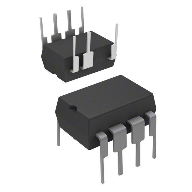
Packages
DIP8
(LC5200D series)
m
m
SOP8
(LC5200S series)
R
ec
o
Not to scale
ot
The product lineup for the LC5200 series provides the following options:
N
Part
Number
LC5202D
LC5202S
LC5205D
Input Voltage, VBB
Absolute
Maximum
(V)
Recommended
Operating Range*
(V)
250
25 to 200
25 to 400
LC5203D
250
25 to 200
LC5210D
450
25 to 400
2.2
6
1.0
*Minimum input voltage of recommended range depends on LED output voltage.
LC5200-DS, Rev. 6.0
RDS(ON)(max)
(Ω)
0.5
450
LC5205S
Output
Current, IO
(A)
SANKEN ELECTRIC CO., LTD.
Package
DIP8
SOP8
DIP8
SOP8
1.3
DIP8
3
DIP8
�LC5200 Series
Off-Line LED Driver ICs
Electrical Characteristics
• The polarity value for current specifies a sink as "+ ," and a
source as “−,” referencing the IC.
ns
• When pin numbers of the SOP8 differ from those of the DIP8,
they are indicated in parentheses for the SOP8.
Symbol
Unit
250
V
450
V
250
V
450
V
0.5
A
1.0
A
2–8
−0.3 to VZ
V
3–8
−0.3 to
VREG + 0.3
V
VSEN
4–8
−0.3 to 4
V
Pins
D
VBB
ew
LC5205D
LC5205S
LC5210D
VO
rN
LC5202D
LC5202S
LC5203D
LC5205D
LC5205S
LC5210D
LC5202D
LC5202S
LC5205D
LC5205S
Pulse width ≥ 1 μs
6–8
(7 – 8)
5–4
(5,6 – 4)
Output Current1
de
d
Output Breakdown Voltage
Notes
LC5202D
LC5202S
LC5203D
fo
Main Power Supply Voltage
Rating
m
Characteristic
es
ig
Absolute Maximum Ratings Unless specifically noted, TA is 25°C
5–4
(5,6 – 4)
en
IO
LC5203D
LC5210D
PWM Pin Voltage2
VPWM
VREF
m
REF Pin Input Voltage
ec
o
SEN Pin Voltage
ot
R
Allowable Power Dissipation3,4
PD
Pulse width ≥ 1 μs
LC5202S
LC5205S
Mounted on Sanken evaluation
board for the SOP8
–
0.85
W
LC5202D
LC5203D
LC5205D
LC5210D
Mounted on Sanken evaluation
board for the DIP8
–
1.73
W
TA
–
−40 to 105
°C
Storage Temperature
Tstg
–
−40 to 150
°C
Channel Temperature
TJ
–
150
°C
N
Operating Ambient Temperature
1The
Output Current rating may be limited by duty cycle, ambient temperature, and heat sinking. Under any set of conditions, do not exceed the
specified junction temperature, TJ .
2V here is the breakdown voltage of the Zener diode that is internally connected between the PWM pin and GND: V = 6.3 V (typ). Maximum input
Z
Z
current is 1 mA.
3Allowable Power Dissipation, P , depends on PWB circuit trace layout.
D
4Refer to the T versus P curve.
A
D
LC5200-DS, Rev. 6.0
SANKEN ELECTRIC CO., LTD.
2
�LC5200 Series
Off-Line LED Driver ICs
2
PD = 1.73 W
Mounted on the corresponding
Sanken evaluation board
1
PD = 0.85 W
0.5
0
0
25
50
75
D
SOP8
RθJA = 147°C/W
es
ig
DIP8
RθJA = 72°C/W
ns
1.5
ew
Maximum Allowable Power Dissipation
PD (W)
TA versus PD Curve
100
125
150
Recommended Operating Conditions*
Symbol
en
Characteristic
de
d
fo
rN
Ambient Temperature, TA (°C)
m
LC5202D
LC5202S
LC5203D
VBB
ec
o
m
Main Power Supply Voltage
IO(AVG)
ot
R
Average Output Current
REF Pin Input Voltage
N
Case Temperature
LC5205D
LC5205S
LC5210D
Notes
Minimum input voltage of the
recommended range depends on
the LED output voltage.
LC5202D
LC5202S
LC5205D
LC5205S
Pins
TC
Normal operation
Center of branded side, TJ ≤ 150°C
Max.
Unit
25
200
V
25
400
V
–
0.4
A
–
0.8
A
6–8
(7 – 8)
5–4
(5,6 – 4)
LC5203D
LC5210D
VREF
Min.
3–8
–
0.8
V
–
–
105
°C
*Recommended operating conditions means operating conditions that maintain normal device functions as shown in the Electrical
Characteristics table.
LC5200-DS, Rev. 6.0
SANKEN ELECTRIC CO., LTD.
3
�LC5200 Series
Off-Line LED Driver ICs
Electrical Characteristics Unless specifically noted, TA is 25°C, VBB = 140 V
Symbol
Test Conditions
Max.
Unit
Output off
6–8
(7 – 8)
―
0.8
1.2
mA
IBB
Normal operation
6–8
(7 – 8)
―
2
―
mA
250
―
―
V
VF
ID = 0.5 A
LC5203D
ID = 1.0 A
LC5205D
LC5205S
ID = 0.5 A
LC5210D
ID = 1.0 A
LC5202D
LC5202S
IF = 0.5 A
LC5203D
IF = 1.0 A
LC5205D
LC5205S
IF = 0.5 A
UVLO Threshold (Turn on)
VUVLO(ON)
UVLO Threshold (Turn off)
VUVLO(OFF)
VREG
REG Pin Output Current
IREG
4–5
(4 – 5,6)
IF = 1.0 A
―
―
V
―
1.2
2.2
Ω
―
0.7
1.3
Ω
―
3.5
6
Ω
―
1.7
3
Ω
―
0.8
1.0
V
―
0.75
1.2
V
―
0.8
0.9
V
―
0.88
1.0
V
6–8
(7 – 8)
―
14
―
V
6–8
(7 – 8)
―
13
―
V
IREG = –0.1 mA
1−8
11.5
12
12.5
V
VREG = 11 V
1−8
―
―
−2
mA
VBB pin
VBB pin
m
m
REG Pin Output Voltage
5–4
(5,6 – 4)
de
LC5210D
es
ig
LC5202D
LC5202S
450
D
RDS(ON)
ID = 1 mA
ew
LC5205D
LC5205S
LC5210D
fo
V(BR)DSS
5–4
(5,6 – 4)
rN
LC5202D
LC5202S
LC5203D
en
Body Diode Forward Voltage
Typ.
d
Output MOSFET On-Resistance
Min.
IBBS
Power Supply Current
Output MOSFET Breakdown Voltage
Pins
ns
Characteristic
VREF
3−8
0
―
1
V
IREF
3−8
−10
―
10
μA
Current Control Detection Voltage
VSEN
4−8
VREF − 0.03
VREF
VREF + 0.03
V
OCP Detection Voltage
VOCP
4−8
―
3
―
V
ISEN
4−8
−10
―
10
μA
REF Pin Input Voltage
R
SEN Pin Current
ec
o
REF Pin Input Current
tBLK
PWM Operation Frequency
fPWM
N
ot
PWM Blanking Time
Duty cycle = 50%
―
―
400
―
ns
2−8
―
―
200
kHz
Output MOSFET Rise Time
tr
IO = 0.4 A
5–4
(5,6 – 4)
―
20
―
ns
Output MOSFET Fall Time
tf
IO = 0.4 A
5–4
(5,6 – 4)
―
50
―
ns
―
°C
Thermal Shutdown Threshold
TTSD
Temperature of Control Part
―
―
150
Thermal Shutdown Hysteresis
TTSD(HYS)
Temperature of Control Part
―
―
55
―
°C
―
―
―
72
°C/W
―
―
―
147
°C/W
LC52xxD
Thermal Resistance
LC5200-DS, Rev. 6.0
RθJA
LC52xxS
Mounted on the
Sanken evaluation
board; the thermal
resistance between
MOSFET and
ambient temperature
SANKEN ELECTRIC CO., LTD.
4
�LC5200 Series
Off-Line LED Driver ICs
Pin List Table
Number
8 GND
REG 1
LC52xxD
(DIP8)
LC52xxS
(SOP8)
REG
1
1
Internal regulator supply, provides current to internal and external circuits;
connect a 0.1 μF bypass capacitor between this pin and GND
PWM
2
2
Input for PWM control; to use internal PWM, connect a CR (capacitor and
resistor) for setting off-time; to use external PWM, connect to PWM signal
source
REF
3
3
Reference voltage input; sets peak output current of OUT pin (internal
power MOSFET) for internal PWM control by REF pin voltage
SEN
4
4
Output current detection; detects peak output current for internal PWM
control, and detects overcurrent for OCP; connect to current detection
resistor, RS
OUT
5
5, 6
VBB
6
7
–
7
GND
8
REG 1
8 GND
PWM 2
7 VBB
REF 3
6 OUT
SEN 4
5 OUT
Drain of internal power MOSFET
Supply voltage; provides power to internal circuits through internal
regulator
LC5200D DIP8 pin removed to increase creepage distance between high
votlage pin and low voltage pin (Note: apply user's criteria for creepage
distance when using LC5200S SOP8)
8
Ground pin
en
de
d
SOP8
LC5200S Series
D
DIP8
LC5200D Series
ew
5 OUT
rN
SEN 4
fo
6 VBB
es
ig
PWM 2
REF 3
Function
ns
Pin-out Diagrams
Name
m
Functional Block Diagram
m
6 (7) VBB
Regulator
PWM
2
REF
3
Current
Control
ot
R
ec
o
REG
1
Control IC
UVLO
Logic
TSD
OUT
5 (5,6)
Gate Driver
N
OCP
SEN
4
8 GND
When pin numbers of the SOP8 differ from those of the DIP8,
they are indicated in parentheses for the SOP8
LC5200-DS, Rev. 6.0
SANKEN ELECTRIC CO., LTD.
5
�LC5200 Series
Off-Line LED Driver ICs
Internal Circuit Descriptions
Undervoltage Lockout (UVLO)
ns
Note: The OCP function is activated only when the SEN pin
voltage, VSEN , reaches VOCP by excessive output current flowing
to RS . Therefore if the output current is restricted to less than its
target value, for example by current limitations of the inductor,
even though the LEDs are shorted, OCP would not be activated.
m
Thermal Shutdown (TSD)
m
en
de
d
This continually monitors whether the output voltage from the
Regulator function is normal, and prevents abnormal operation
resulting from low input voltage. When the VBB pin voltage is
lower than the UVLO threshold (Turn-off), VUVLO(OFF) , the IC
reverts to the state before startup. In addition, this function is
available during power-on reset, for releasing latched shutdowns
resulting from operation of protection functions.
rN
The output current is controlled constant in internal PWM mode,
by comparing the REF pin voltage with the SEN pin voltage.
fo
Current Control
Overcurrent Protection (OCP)
The drain current is detected by the current detection resistor,
RS . When the SEN pin voltage, VSEN , reaches the OCP detection
voltage, VOCP , or more, the OCP function is activated, and thus
the output of the OUT pin turns off, in latch mode. To release
latch mode, cycling power to the IC (that is, the VBB pin voltage falling down to VUVLO(OFF) and then rising to VUVLO(ON)) is
required.
ew
This regulator steps-down from the supply voltage, VBB , to 12 V,
and provides power to internal circuits and external devices. A
ceramic capacitor of 0.1 μF should be connected close to the
REG pin to stabilize operation because some pulse currents flow
through the gate capacitor when charging the internal power
MOSFET.
es
ig
Regulator
Because this circuit is in the Control Part, there is a delay
before temperature increases in the internal power MOSFET are
conducted to the Control Part. If the temperature of the power
MOSFET increases rapidly, the power MOSFET may be damaged before TSD is activated. Therefore, it is necessary design
the application well to protect against this.
D
This section describes the functions displayed in the Functional
Block diagram.
Gate Driver Operation
Gate driver for internal power MOSFET.
Internal Power MOSFET
An internal power MOSFET for LED driving is incorporated in
the IC series, according to the individual product ratings for current and voltage.
N
ot
R
ec
o
This continually monitors the chip temperature of the Control
Part. When the temperature increases to TTSD or higher, the
output of the OUT pin turns off to prevent damage from abnormally high temperature. After TSD operation, when the temperature decreases to TTSD minus TTSD(HYS) or lower, or after cycling
power to the IC (that is, the VBB pin voltage falling down to
VUVLO(OFF) and then rising to VUVLO(ON) ), the IC returns to normal operation.
Logic
This controls the enabling and disabling of the output of the OUT
pin according to signals from the current control circuit and/or
the various protection circuits. The output is enabled only when
the operation is normal and the current control circuit outputs the
on-signal for the OUT pin.
LC5200-DS, Rev. 6.0
SANKEN ELECTRIC CO., LTD.
6
�LC5200 Series
Off-Line LED Driver ICs
ns
Typical Application Circuit
U1
CIN
Line
Filter
REG VBB
C2
LC5200
REF
PWM
OUT
SEN
CPWM
GND
VLED
L1
RS
rN
R2
C1
D
RPWM
R1
D1
ew
AC
Input
es
ig
VIN
N
ot
R
ec
o
m
m
en
de
d
fo
Figure 1. Typical application circuit example for a buck configuration; for component values,
see Application Information section
LC5200-DS, Rev. 6.0
SANKEN ELECTRIC CO., LTD.
7
�LC5200 Series
Off-Line LED Driver ICs
Package Diagrams
DIP8
1
4
es
ig
5
ew
rN
+0.3
1.52
-0.05
(7.6 TYP)
3.3 ±0.2
m
m
en
7.5 ±0.5
de
4.2 ±0.3
d
3.4 ±0.1
fo
1.0 +0.3
-0.05
D
6.5 ±0.2
8
ns
9.4 ±0.3
0.2 5 + 0.
- 0.01
5
0~15° 0~15°
ec
o
2.54 TYP
0.5 ±0.1
R
0.89 TYP
ot
Unit: mm
N
8
LC52xx
SK YMW
XXXX
Pb-free. Device composition compliant
with the RoHS directive.
LC5200-DS, Rev. 6.0
1
SANKEN ELECTRIC CO., LTD.
Part Number
Lot Number
Y is the last digit of the year (0 to 9)
M is the month (1 to 9, O, N, or D)
W is week code (1 to 3)
Sanken Control Number
8
�LC5200 Series
Off-Line LED Driver ICs
SOP8
5.2 ±0.3
1
rN
ew
D
6.2 ±0.3
es
ig
ns
5
4.4 ±0.2
8
4
0 to 10°
fo
0.695 TYP
m
en
+0.1
0.15 –0.05
de
1.5 ±0.1
d
5.25 ±0.3
ec
o
0.05 ±0.05
m
1.27±0.05
0.10
0.4±0.1
ot
R
0.12 M
0.4±0.2
N
Unit: mm
8
LC52xx
SK YMW
Pb-free.
Device composition compliant
with the RoHS directive.
XXXX
1
LC5200-DS, Rev. 6.0
Part Number
Lot Number
Y is the last digit of the year (0 to 9)
M is the month (1 to 9, O, N, or D)
W is week code (1 to 3)
Sanken Control Number
SANKEN ELECTRIC CO., LTD.
9
�LC5200 Series
Off-Line LED Driver ICs
Functional Description
• All of the parameter values used in these descriptions are typical
values, unless they are specified as minimum or maximum.
Internal PWM Control Circuit
Figure 3 shows the internal PWM control circuit, and figure
4 shows the timing diagram of that circuit. When the power
MOSFET turns on, both the load current and VSEN across the current detection resistor RS increase.
REG
Turning-Off Period
The output current through the LED string is equivalent to the
current through the detection resistor, RS, and thus the LED current is detected at the SEN pin as a voltage. When the SEN pin
voltage, VSEN, is equal to the REF pin voltage, VREF, the internal
power MOSFET turns off.
RPWM
rN
fo
Comp1
S
+
Q
R
6V
REF
+ Comp2
VREF
Blank Pulse
-
I
O
d
de
en
m
ION
-
PWM
CPWM
LC5200
2V
ew
3V
PWM Off-Time Period
When the internal power MOSFET turns off, the current recirculation diode, D1, is forward biased by the back electromotive
force (BEMF) in the inductor, L1, and D1 turns on. Then the
energy stored in L1 during PWM on-time flows through the recirculation path shown as IOFF in figure 2.
VIN
D
es
ig
PWM On-Time Period
At startup, or during normal operation before the output current through the LED string reaches the target current level, the
internal power MOSFET turns on and the output current flows
through the ION path shown in figure 2.
Turning-On Period
After the fixed off-time, tOFF , the internal power MOSFET turns
on again, and the PWM on-time period repeats. The cycle is
shown in figure 2 panel B.
ns
PMW Current Control (Buck Converter)
• The polarity value for current specifies a sink as "+ ," and a
source as “−,” referencing the IC.
OUT
To LED load
Logic
Gate Driver
SEN
RS
GND
D1
V LED
ec
o
(A)
LC5200
LED
m
IOFF
OUT
R
MOSFET
SEN
ot
GND
L1
LED Current
ILED
RS
VREF
VSEN
LED current
ILED
(B)
ION
I OFF
I ON
I OFF
ION
Comp2
DS
EN
DS
EN
tBLK
IOFF
DS
t BLK
Negative IN
OT Comp
OUT
ON
OFF
tOFF
Figure 2. Current Control of Buck Converter
LC5200-DS, Rev. 6.0
IOFF
Comp1
VREF
VSEN
MOSFET
ION
Comp2
OUT
N
GND
VSEN
Figure 3. Current Control Circuit
OFF
MOSFET
ON
V PWM
ON
OFF
ON
A
t OFF
B
Figure 4. Current Control Circuit Timing Chart
SANKEN ELECTRIC CO., LTD.
10
�LC5200 Series
Off-Line LED Driver ICs
D
VREF
VREG × R2
=
RS
RS × ( R1 + R2 )
(1)
ew
IPEAK =
The LC5200 series allows external adjustment of the current
flowing through the LED string, using either of the following
methods:
rN
When VPWM increases to more than 3 V, the fixed off-time
expires and the power MOSFET turns on. After that, the operation reverts to the initial state, shown as point B in figure 4.
• Adjusting the analog voltage on the REF pin (figure 6A)
• Inputting the analog voltage integrated PWM signal through a
low pass filter, LPF, to the REF pin (figure 6B)
fo
VSEN is detected in the on-time period, except during the PWM
blanking time, tBLK , in order to prevent malfunction.
Using Internal PWM Dimming
The LC5200 series has a built-in PWM constant current control
circuit, and thus can achieve a constant current drive system for
the LED string, while requiring few external components. The
peak output current, IPEAK , for driving the LED string is calculated as follows:
es
ig
After a certain period, when the PWM pin voltage, VPWM ,
decreases to less than 2 V, the comparator for the off-time,
Comp1, inverts and the Q output of the RS flip-flop is set. Then
the MOS switch for discharging CPWM turns off, and CPWM
is charged by the REF pin voltage through RPWM (connected
between the REF and PWM pins).
Current Value Setting for Dimming Control
The LC5200 series allows constant current control using the
internal PWM control, an external PWM signal, or a combination
of both of them.
ns
Comp2 compares VSEN and VREF , and when VREF < VSEN ,
Comp2 inverts its output (see point A in figure 4). This resets the
output Q of the RS flip-flop. After a turn-off signal is transmitted
from the AND gate to the logic, to the gate driver, and finally to
the internal power MOSFET, the power MOSFET turns off. At
the same time, an internal MOS switch, connected to the PWM
pin, turns on, and CPWM is discharged.
However, the dimming control by adjusting the REF pin voltage
can not set the output current to zero. When controlling to zero
current, an external signal and external circuit are needed to set
the PWM pin voltage to low.
m
en
de
d
The fixed off-time is determined by RPWM and CPWM. Figure 5
shows PWM off-time curves based on various values of RPWM
and CPWM . The recommended value for RPWM is 560 kΩ, and that
for CPWM is 220 pF. In addition, the proper values for RPWM and
CPWM are changeable according the load conditions of the LEDs
used, and the value of RPWM also affects the losses in the internal
regulator directly. It is necessary to pay attention to these factors.
REG
RPWM
LC5200
C1
ec
o
m
R1
10
R
R2
C2
0 pF
(A) Analog Control
= 220 pF
0 pF
C PWM = 47
pF
C PWM = 22
pF
C PWM = 10
pF
REG
LPF
RLPF
560
CLPF
600
800
LC5200
REF
PWM
GND
CPWM
SEN
RS
1000
(B) Integrated PWM Control
RPWM Value for Setting Off-Time (Ω)
Figure 5. PWM Off-Time versus RPWM Value, for Various Values of CPWM
LC5200-DS, Rev. 6.0
RPWM
PWM
Signal
2
400
SEN
RS
C PWM = 10
5
1
200
GND
CPWM
C PWM = 47
C PWM
ot
20
N
Internal PWM Off-Time, tOFF (μs)
50
REF
PWM
Figure 6. Dimming Application Circuits with Internal PWM Control
SANKEN ELECTRIC CO., LTD.
11
�LC5200 Series
Off-Line LED Driver ICs
PWM
Signal
OUT
GND
SEN
en
REF
PWM
m
RS
OUT Pin
ns
es
ig
RPWM
LC5200
R1
REF
MOS
Switch
PWM
Signal
VBB
OUT
PWM
GND
CPWM
SEN
R2
RS
PWM Pin Signal
LED Current Control
Off
L
Internal PWM current control
On
H
LED current off
R
ec
o
L
H
REG
Truth Table for Combined Internal and External PWM
m
Truth Table for External PWM
PWM Pin Signal
D
de
LC5200
100 kΩ
As shown in figure 8, the circuit has an added external MOS
switch, and when the PWM pin signal goes low, the internal
PWM current control is activated.
d
VBB
REG
The narrower the duty cycle of the external PWM signal is, the
higher the average LED output current is. At a 100% duty cycle,
the LED output current is 0 A. The timing diagram is shown in
figure 9.
fo
On the internal circuit of the PWM pin, there is a comparator
with hysteresis. When the input signal on the PWM pin is 3 V, the
comparator turns on the OUT pin, and when the input signal is
2 V, the comparator turns off the OUT pin. Because the internal
circuit of the PWM pin has a built-in Zener diode of 6.3 V (typ)
for protection, the PWM pin voltage is compatible with 5 V
CMOS logic level.
Using Both Internal and External PWM Dimming
This configuration combines the two configurations described
above: the internal PWM control circuit determines the limitation
of the peak output current flowing through the LED string, and
the external PWM circuit controls the average current. This configuration is effective for a low frequency external PWM range,
200 to 500 Hz. The application circuit is shown in figure 8.
ew
As shown in figure 7, CPWM and RPWM are removed, and then the
PWM signal is directly input to the PWM pin. The REF pin must
be pulled up to the REG pin.
When the SEN pin voltage, VSEN, reaches the OCP detection
voltage, VOCP, or more, the OCP function is activated.
rN
Using External PWM Dimming
Using an external PWM signal allows applying the LC5200
series as a high voltage power switch. In this configuration, the
output of the OUT pin turns on and off according to a logic signal
input to the PWM pin. Because this control is not activated by the
internal PWM current control circuit, an external current control
circuit is needed. The frequency of the input PWM signal is recommended to be in the range 20 to 200 kHz.
Figure 8. Dimming Application Circuit with Combined Internal and External
PWM Control
N
ot
Figure 7. Dimming Application Circuit with External PWM Control
PWM
VPWM
LED
ILED
IC
Internal PWM
OFF
Figure 9. Timing for Combined Internal and External PWM Operation
LC5200-DS, Rev. 6.0
SANKEN ELECTRIC CO., LTD.
12
�LC5200 Series
Off-Line LED Driver ICs
Application Information
ns
es
ig
ew
D
In actual operation, L1 should be rated such that it is not saturated
by the peak of the ripple current. If the inductor becomes saturated by an unexpectedly high surge current flow, the LEDs and
the IC could be damaged.
D1
This is a free-wheeling diode for recirculation of the output
current. The energy stored during the PWM on-time period is
provided to the LEDs through this diode during the off-time
period. The withstand voltage and the recovery time, tRR , should
be considered.
m
en
de
d
LEDs
The relationship between the LED ratings and the output current ratings of the IC should be considered. In a buck configuration, the total forward voltage drop, VLED , of the LEDs in series
L1
This is an inductor for smoothing output current. When the
inductance value of L1 is relatively higher, the LED ripple current
is lower, and thus current stability is improved. Normally, an L1
value of 0.5 to 10 mH is assumed.
fo
External Component Selection
The following recommendations should be observed when selecting components for use with the LC5200 series.
should be less than the VBB pin voltage, VBB , because the LEDs
would be turned off if VLED were more than VBB . Normally, a
VLED of 9 to 60 V is assumed.
rN
Typical Application Components
The typical application circuit for a buck configuration, shown
in figure 1, is an example for a basic peripheral circuit. Table 1
provides reference specifications for the typical application
circuit in figure 1, listing parts as examples for the sole purpose
of reference for the initial use of the IC. The specifications are
for typical values, and do not take into consideration application
usage conditions such as PCB layout, LED types, or circuit noise.
It is necessary to take account of such factors fully while designing the application, and component selection should be validated
by operation in the actual application.
m
Table 1. Reference Specification of the Typical Application Circuit
Symbol
L1
Part Type
Reference Values
and Rating
LED
–
R
LED
ec
o
Input voltage: 100 VAC, LED output voltage: 5 LEDs in series (about 15 to 18 V total), LED peak output current: 0.35 A
1 mH / 1 A
D1
SJPD-L5
CIN
Capacitor
C1
Capacitor
ot
Inductor
Fast Recovery
Rectifier Diode
N
Description
User-defined
Up to 4.7 μF / 450 V
0.1 μF / 25 V
Choke coil for smoothing current
Free-wheeling diode for recirculation
Main supply source filtering capacitor
Internal regulator stabilizing capacitor
C2
Capacitor
0.1 μF / 25 V
RPWM
Resistor
560 kΩ / 1/8 W
PWM off-time setting resistor for internal PWM control
CPWM
Capacitor
220 pF / 25 V
PWM off-time setting capacitor for internal PWM control
R1
Resistor
680 kΩ / 1/8 W
Resistor for setting peak output current on OUT pin
R2
Resistor
20 kΩ /
1/ W
8
Resistor for setting peak output current on OUT pin
RS
Resistor
1.0 Ω / 1 W
LC5200-DS, Rev. 6.0
REF pin voltage stabilizing capacitor
Resistor for output current detection
SANKEN ELECTRIC CO., LTD.
13
�LC5200 Series
Off-Line LED Driver ICs
ns
VREF
VREG × R2
=
RS
RS × ( R1 + R2 )
es
ig
For example, to set IPEAK to 0.35 A, assuming a REG pin voltage,
VREG , of 12 V, and resistances for R1 of 680 kΩ, R2 of 20 kΩ,
and RS of 1 Ω:
IPEAK =
12 (V) × 20 (kΩ)
1 (Ω) × ( 680 (kΩ) × 20 (kΩ) )
= 0.343 A
In actual operation, the current value is higher than that calculated by the above equation because there is some propagation
delay in internal circuit. Especially when the input voltage is
high and the inductance value is low, the di/dt slope of the current is high, and the actual current value is much higher than the
calculated current value. The current flowing to R1 and R2 affects
the losses in the internal regulator directly. Therefore it is recommended to select R1 and R2 such that 500 kΩ < R1 + R2 , in order
to restrict current as much as possible.
d
fo
Note: If the lower peak of the ripple voltage of VIN is allowed to
fall below the UVLO Threshold (Turn off), VUVLO(OFF) , or if the
output voltage is less than VLED , the LEDs are turned off. Thus it
is necessary to take account of the value of CIN .
IPEAK =
D
The IC is capable of operation, with VIN full-wave rectification,
with an input capacitor rated as low as approximately 1000 pF,
instead of with an electrolytic capacitor. By allowing configuration without an electrolytic capacitor, the IC enhances power supply system operational life, and reduces system size and cost.
These resistors determine the peak output current, IPEAK , flowing
to the LEDs. The peak current value can be calculated as follows:
ew
CIN
This is an input smoothing capacitor. When the capacitance value
of CIN is relatively higher, the input and output ripple voltages
are lower. However, given a certain capacitance level, the greater
the output power is, the greater the ripple voltages are. Thus it is
necessary to select the value according to the output power.
R1, R2, and RS
rN
If a diode with a long tRR is selected, surge current may flow into
the OUT pin when the internal power MOSFET turns on. If this
were to occur, it would cause increased noise, potentially resulting in malfunction due to the noise, and decreased efficiency.
ec
o
m
m
en
de
C1
This is a capacitor for stabilizing the internal regulator. It is
required to provide the charge current for charging the gate of
the internal power MOSFET, and to maintain a stable voltage.
Normally, a ceramic capacitor of 0.1 μF is used. A too-low value
causes decreased switching speed and malfunctions. A too-high
value causes a longer startup time because a long charging time
for this capacitor delays startup for the power supply. These factors should be carefully evaluated.
RPWM and CPWM
Refer to the PWM Current Control (Buck Converter) section.
N
ot
R
The capacitor should be placed as close to the IC as possible.
It is recommended that the detection resistor, RS , have an allowable power dissipation that is twice to three times as much as
the loss in RS as margin, because the output current flows to it
when the internal power MOSFET turns on, and the loss may be
comparatively large.
LC5200-DS, Rev. 6.0
SANKEN ELECTRIC CO., LTD.
14
�LC5200 Series
Off-Line LED Driver ICs
fo
rN
ew
D
es
ig
ns
Electrostatic Discharge
• When handling the products, the operator must be
grounded. Grounded wrist straps worn should have at
least 1 MΩ of resistance from the operator to ground to
prevent shock hazard, and it should be placed near the
operator.
• Workbenches where the products are handled should be
grounded and be provided with conductive table and floor
mats.
• When using measuring equipment such as a curve tracer,
the equipment should be grounded.
• When soldering the products, the head of soldering irons
or the solder bath must be grounded in order to prevent
leak voltages generated by them from being applied to the
products.
• The products should always be stored and transported in
Sanken shipping containers or conductive containers, or
be wrapped in aluminum foil.
N
ot
R
ec
o
m
m
en
de
d
Because reliability can be affected adversely by improper
storage environments and handling methods, please observe
the following cautions.
Cautions for Storage
• Ensure that storage conditions comply with the standard
temperature (5°C to 35°C) and the standard relative
humidity (around 40% to 75%); avoid storage locations
that experience extreme changes in temperature or
humidity.
• Avoid locations where dust or harmful gases are present
and avoid direct sunlight.
• Reinspect for rust on leads and solderability of the
products that have been stored for a long time.
Cautions for Testing and Handling
When tests are carried out during inspection testing and
other standard test periods, protect the products from
power surges from the testing device, shorts between
the product pins, and wrong connections. Ensure all test
parameters are within the ratings specified by Sanken for
the products.
Soldering
• When soldering the products, please be sure to minimize
the working time, within the following limits:
▫ DIP8
Flow soldering:
260±5°C
10±1 s (2 times)
Soldering iron:
380±10°C 3.5±0.5 s (1 time)
Soldering should be at a distance of at least 1.5 mm
from the body of the products.
▫ SOP8
Reflow soldering:
180°C
90±30 s for preheating
250°C
10±1 s (260°C peak, 2 times) for
solder heating
Soldering iron:
380±10°C 3.5±0.5 s (1 time)
Note: Flow soldering must not be used.
LC5200-DS, Rev. 6.0
SANKEN ELECTRIC CO., LTD.
15
�LC5200 Series
D
es
ig
ns
Off-Line LED Driver ICs
ew
• The contents in this document are subject to changes, for improvement and other purposes, without notice. Make sure that this is the
latest revision of the document before use.
rN
• Application and operation examples described in this document are quoted for the sole purpose of reference for the use of the products herein and Sanken can assume no responsibility for any infringement of industrial property rights, intellectual property rights or
any other rights of Sanken or any third party which may result from its use.
d
fo
• Although Sanken undertakes to enhance the quality and reliability of its products, the occurrence of failure and defect of semiconductor products at a certain rate is inevitable. Users of Sanken products are requested to take, at their own risk, preventative measures
including safety design of the equipment or systems against any possible injury, death, fires or damages to the society due to device
failure or malfunction.
de
• Sanken products listed in this document are designed and intended for the use as components in general purpose electronic equipment or apparatus (home appliances, office equipment, telecommunication equipment, measuring equipment, etc.).
m
en
When considering the use of Sanken products in the applications where higher reliability is required (transportation equipment and
its control systems, traffic signal control systems or equipment, fire/crime alarm systems, various safety devices, etc.), and whenever
long life expectancy is required even in general purpose electronic equipment or apparatus, please contact your nearest Sanken sales
representative to discuss, prior to the use of the products herein.
ec
o
m
The use of Sanken products without the written consent of Sanken in the applications where extremely high reliability is required
(aerospace equipment, nuclear power control systems, life support systems, etc.) is strictly prohibited.
ot
R
• In the case that you use Sanken products or design your products by using Sanken products, the reliability largely depends on the
degree of derating to be made to the rated values. Derating may be interpreted as a case that an operation range is set by derating the
load from each rated value or surge voltage or noise is considered for derating in order to assure or improve the reliability. In general,
derating factors include electric stresses such as electric voltage, electric current, electric power etc., environmental stresses such
as ambient temperature, humidity etc. and thermal stress caused due to self-heating of semiconductor products. For these stresses,
instantaneous values, maximum values and minimum values must be taken into consideration.
N
In addition, it should be noted that since power devices or IC's including power devices have large self-heating value, the degree of
derating of junction temperature affects the reliability significantly.
• When using the products specified herein by either (i) combining other products or materials therewith or (ii) physically, chemically
or otherwise processing or treating the products, please duly consider all possible risks that may result from all such uses in advance
and proceed therewith at your own responsibility.
• Anti radioactive ray design is not considered for the products listed herein.
• Sanken assumes no responsibility for any troubles, such as dropping products caused during transportation out of Sanken's distribution network.
• The contents in this document must not be transcribed or copied without Sanken's written consent.
LC5200-DS, Rev. 6.0
SANKEN ELECTRIC CO., LTD.
16
�


 工商网监
湘ICP备2023018690号
工商网监
湘ICP备2023018690号
