SE4120S
GNSS Receiver IC
Product Description
Applications
!
!
!
!
!
The SE4120S is a highly-integrated GNSS radio front
end IC offering high performance and low power
operation in a wide range of low-cost applications. It
supports GPS and dual-mode L1-band GPS/Galileo
products.
The SE4120S features a conditioned
interface for software implementations of GNSS
baseband signal processing.
Dual-mode GPS and Galileo receivers
Software-defined GNSS radio systems
High sensitivity / low power GNSS / A-GNSS apps.
Portable navigation devices, mobile phones, and
GNSS peripheral devices
Telematics equipment
Features
!
!
!
!
!
!
!
!
!
!
The SE4120S includes an on-chip LNA, a low IF
receiver with a linear AGC and an advanced multi-bit
I/Q analog to digital converter (ADC) with serialized
data output. The receiver incorporates a fully integrated
image reject mixer, obviating the need for a SAW filter
in many applications. The SE4120S’s on-chip IF filter
may be adjusted from 2.2 MHz BW (for GPS only) to
4.4MHz BW (for simultaneous reception of Galileo and
GPS signals). The digitized I/Q output, centered nearzero IF, is available in a serialized data stream to
facilitate software signal processing.
Single conversion L1-band GPS/Galileo radio with
integrated IF filter
2-bit serialized digital I/Q output at near-zero IF
Integrated LNA with high-gain (18.5 dB typ.) and
low NF (1.65 dB typ.)
Very low 2.15 dB typ. RF system noise figure
Low 10 mA operating current with 2.7-3.6 V supply;
8 mA with internal LNA disabled
Low standby current 3 !A typical
Fully integrated VCO and resonator
Integrated PLL supporting 16.368 MHz reference
frequency
I/O supply range extends down to 1.7 V
2.2 x 2.2 x 0.35 mm, 46 pad, 250um pitch, SnAg
solder bump, RoHS-compliant package
The highly-integrated PLL synthesizer of the SE4120S
requires only two passive components to implement an
off-chip loop filter.
The SE4120S is optimized for the lowest possible
power consumption consistent with a very low external
component count.
Ordering Information
Part No.
Package
Remark
SE4120S-R
46-Pad Chip-Scale
Package
Shipped in Tape
& Reel
The SE4120S incorporates current-controlled lowspurious output buffers which may be run from a
separate external supply to interface to low voltage
systems. Output buffers supply sufficient current to
drive most baseband devices directly.
Functional Block Diagram
Optional
filter
LNA_OUT
MIX_IN
VAGC
-45°
~
~
~
Buffer
LNA
I
AGC_DIS
AGC
Controller
IF Filter
DATA_OUT
ADC
Data
Downconverter /
Serializer
+45°
FILT_BW
Q
LNA_IN
CLK_OUT
Sample
Clock
divider
Quadrature
!2
FILT_BW
Feedback
Divider
Fs_SEL1
VCO
SE4120
SYNC
~
Chip
Control
Phase/Frequency
Detector
RX_EN
Reference
Divider
~
Fs_SEL0
OSC_EN
Reference
Oscillator
/ Buffer
RVI
VTUNE
PLL Loop
Filter
DST-00118 ! Rev 4.3 ! May-26-2009
XTAL1/
TCXO IN
XTAL2
1 of 24
�SE4120S
GNSS Receiver IC
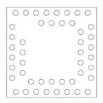
Pad Diagram
36
37
38
40
39
35
42
44
41
43
46
45
1
2
3
SE4120S
34
4
33
5
6
32
31
7
30
8
29
9
Top View
28
10
27
26
11
23
21
19
17
15
12
25
24
22
20
18
16
14
13
1
46
44
42
40
38
37
36
45
2
43
41
39
35
SE4120S
34
3
4
33
5
6
32
31
7
8
30
9
29
Bottom View
10
28
27
11
12
13
15
14
DST-00118 ! Rev 4.3 ! May-26-2009
17
16
19
18
21
20
23
22
26
24
25
2 of 24
�SE4120S
GNSS Receiver IC
Pad Description
Pad
1
Label
VCC_LNA
Function
Analogue power supply for LNA
Connection
Connect to VCC via dedicated decoupling
network, to enable LNA.
Connect to GND to disable LNA
2
GND
GND connection
Connect to GND
3
VCC_AGC
Analogue power supply for AGC
Connect to VCC
4
LNA_IN
LNA RF input
DC blocking capacitor required. Connect to
matching network in a compact RF layout.
5
GND
GND connection
6
GND
GND connection
7
NC
(reserved)
8
GND
GND connection
9
GND
GND connection
10
GND
GND connection
11
VDD_FSE1
Power supply for configuration logic
12
VDD_FSE2
Power supply for configuration logic
13
VAGC
AGC filter capacitor
14
RX_EN
Receiver enable
15
AGC_DIS
AGC Inhibit Input
Connect to GND
Leave unconnected
Connect to GND
Connect to VCC
Single capacitor to GND
(Pad also allows external control of AGC when
AGC_DIS=’1’)
Connect to VDD level to enable Radio
Connect to VSSN / GND to disable Radio
AGC Gain hold (Connect to VDD)
or
Enable AGC (Connect to VSSN / GND)
16
VSSN
Ground return for digital interface
Connect to GND, or digital ground for
baseband IC
17
VDDN
Digital power supply for digital interface
Connect to VDD, or digital supply for
baseband IC
18
NC
(reserved)
19
NC
(reserved)
20
GND
GND connection
Connect to GND
Leave unconnected
21
Fs_SEL0
Serial IF data output select (bit 0)
Select desired serial data output, sample rate,
and format, as per “Fs_SEL Hardware
Configuration” Table (Connect to RX_EN (pad
14) or VSSN / GND as required)
22
CLK_OUT
Sample clock output
ADC Sample Clock output, at VDDN logic
levels
23
DATA_OUT
Serialized IF data output
ADC serial I/Q output at VDDN logic levels
24
SYNC
IF data sync output
ADC data Sync output at VDDN logic levels
DST-00118 ! Rev 4.3 ! May-26-2009
3 of 24
�SE4120S
GNSS Receiver IC
Pad
Label
Function
Connection
25
FILT_BW
IF filter bandwidth select
Connect to RX_EN (pad 14) for dual-mode
Galileo+GPS operation
Connect to VSSN / GND for GPS only
26
Fs_SEL1
Serial IF data output select (bit 1)
Select desired serial data output, sample rate,
and format, as per “Fs_SEL Hardware
Configuration” Table (Connect to RX_EN (pad
14) or VSSN / GND as required)
27
NC
(reserved)
Leave unconnected
28
XTAL1
Crystal/TCXO connection
If using TCXO reference source:
Connect to AC coupled TCXO reference signal
If using Crystal reference source:
Connect to Crystal input 1 (XTAL1)
29
GND
GND connection
Connect to GND
30
XTAL2
Crystal connection
If using TCXO reference source:
Leave unconnected
If using Crystal reference source:
Connect to Crystal input 2 (XTAL 2)
31
VSSQ
Ground return for quiet digital circuits
Connect to GND
32
VDDQ
Power supply for quiet digital circuits
Connect to VCC
33
VSSCP
Ground return for PLL Charge-Pump
Connect to GND
34
VDDCP
Power supply for PLL Charge-Pump
Connect to VCC
35
VTUNE
VCO tuning voltage input / PLL Charge
pump output
Connect to PLL filter network
36
GND
GND connection
Connect to GND
37
GND
GND connection
Connect to GND
38
MIX_IN
Mixer input
DC coupled RF input to RF Mixer
39
OSC_EN
Crystal oscillator enable
If using TCXO reference source (NO crystal
oscillator needed):
Connect to VSSN / GND
If using Crystal reference source, with crystal
oscillator:
Connect to VDDN
40
GND
GND connection
Connect to GND
Leave unconnected
or
Connect to via resistor to analogue VCC for up
to 2x output drive current
41
RVI
Program baseband output drive current
42
VCC_RF
Analogue power supply for RF blocks
43
VCC_RF
Analogue power supply for RF blocks
44
GND
GND connection
Connect to GND
45
NC
(reserved)
Leave unconnected
46
LNA_OUT
LNA RF output
RF output from LNA. DC blocked, with 10 k"
(nom) DC impedance to ground.
DST-00118 ! Rev 4.3 ! May-26-2009
Connect both pads to VCC
4 of 24
�SE4120S
GNSS Receiver IC
Functional Description
LNA
LNA performance is the largest single contributor to
overall system sensitivity in both GPS and Galileo
signal reception. The internal LNA of the SE4120S
allows excellent performance to be achieved from a
low-power GNSS receiver without requiring any
additional active components.
The Galileo and GPS L1 input signals are both
centered on 1575.42 MHz, and can be simultaneously
applied to LNA_IN (pad 4).
The SE4120S LNA input requires a minimum of
external matching components to achieve good RF
gain with minimal noise figure: only a single series
inductor and single shunt capacitor are required. The
input requires a DC blocking cap if circuitry prior the
LNA has a DC bias. Although attention should be paid
to track lengths and interference throughout the
design, the LNA input matching circuit is the only RF
circuit critically sensitive to layout.
The LNA output includes internal 50 "#matching for
connection to the mixer input either directly or via an
optional external filter.
In applications where the internal LNA is not needed,
the LNA can be disabled by connecting VCC_LNA
(pad 1) to GND. This will save approximately 1.9 mA
of active current.
Mixer RF Input
The mixer RF input, MIX_IN (pad 38), is a single
ended 50 " input, designed to interface either to
LNA_OUT (pad 46) or to the output of an external
filter. An external active antenna can also be
connected to the mixer input.
The image reject mixer ensures that the receiver’s full
sensitivity is achieved without an external filter. For
applications where additional selectivity is required,
an external filter can be added between the
LNA_OUT and MIX_IN pads.
IF Filter
The SE4120S includes a fully integrated Intermediate
Frequency (IF) filter which provides excellent
interference rejection with no additional external
components. The filter has a 3rd order Butterworth
bandpass response.
The IF filter operates in two modes. In one mode,
Galileo and GPS signals are allowed to pass; in the
other, only GPS signals are captured. The two modes
can be set by a Logic ‘1’ on FILT_BW (pad 25) for
Galileo + GPS (4.4 MHz BW), and a Logic ‘0’ on the
DST-00118 ! Rev 4.3 ! May-26-2009
same pin for GPS only (2.2 MHz BW). In both cases,
the nominal center frequency of the filter is preset to
4.092 MHz.
AGC and ADC
The SE4120S features a linear IF chain with a multibit analogue-to-digital converter (ADC).
An Automatic Gain Control (AGC) system is included.
This provides gain control over a range greater than
40 dB so that signals are presented at an optimum
level to the input of the ADC.
The ADC quantizes the IF signal into a traditional 2-bit
real digital IF data comprising MAG and SIGN
components. The MAG values control the AGC loop,
such that the MAG bit is active (HIGH) for
approximately 33% of the time.
The SIGN and MAG signals are fed into a data
downconverter and serializer, which in turn generates
I/Q digital data that is ultimately available from
DATA_OUT (pad 23). Refer to the “Digital Down
Sampler” section below for further information.
The AGC time constant is determined by a single
external capacitor connected between the VAGC pin,
and VSSN / GND. The settling-time of the AGC is
within 10 ms with a 10nF capacitor.
The AGC system also features a control-inhibit
facility, via AGC_DIS (pad 15). By connecting
AGC_DIS to VDDN, the internal AGC controller is
inhibited and the gain held at the level set prior to the
inhibition. While the AGC controller is inhibited, it is
possible to control the AGC gain from an external
source by applying a low-impedance voltage to VAGC
(pad 13).
Digital Downconverter / Serializer
The SE4120S includes a digital signal conditioning
and serial interface function which prepares the
digitized GNSS signal data for baseband signal
processing. This interface provides a near-zero IF
signal data at a minimum data rate and formatted for
efficient processing via synchronous serial interface
hardware commonly found on microprocessor
integrated circuits.
The
2-bit
real
IF
data
input
to
the
Downconverter/Serializer is downconverted and
represented as 2-bit in-phase (I) and 2-bit quadrature
(Q) components of the signal bandwidth centered at
near-zero frequency (0 Hz when using a 16.368 MHz
reference).
5 of 24
�SE4120S
GNSS Receiver IC
To allow the lowest possible sample rate, the
downconverted IF signal is further filtered to re-shape
the noise spectrum and remove any significant
degradation from aliasing. Both frequency conversion
and filtering functions are performed digitally, avoiding
the tolerance, offset and imbalance imperfections
associated with analogue converters.
The output data is can be presented in two ways:
1)
a series of 8-bit streams of alternating I and
Q samples with an Active LO SYNC framing
pulse at the beginning of every 8 bits of data.
This format is referred to as “Byte Sync.”
2)
a continuous stream of alternating I and Q
samples with an Active HI SYNC pulse
coinciding with every SIGN I bit. This format
is referred to as “Pulse Sync.”
Each sample is presented as alternate I & Q bit
values. In 2-bit I/Q mode, a single bit is allocated to I
and a single bit allocated to Q. In 4-bit I/Q mode, a
SIGN bit and a MAG bit are allocated to each of the I
& Q samples.
Serial Data Output format / Sampling
Frequency Selection
The serial IF data output is available on a three-wire
bus system comprising a single-bit DATA_OUT
(pad 13), SYNC (pad 24) and CLK_OUT (pad 22).
The output of the data can be configured to be either
Byte Sync (distinct 8-bit sequences of data) or Pulse
Sync (continuous datastream). The data which is
encoded in these formats is derived from the internal
ADC in either 2-bit I/Q (1-bit I & 1-bit Q) or 4-bit I/Q (2bit I and 2-bit Q). Diagrams showing Pulse Sync and
Byte Sync serial data appear below.
DST-00118 ! Rev 4.3 ! May-26-2009
The following truth table gives the permutations for
the serial IF data output. The required configuration
may be set by wiring the Fs_SEL[1:0] pads (26, 21)
HIGH or LOW to select the required mode. In each of
the modes, the same frequency appears at CLK_OUT
(pad 22), but in Byte-Sync, wait-states (clock-idle
cycles) will be inserted.
Fs_SEL Hardware Configuration
Fs_SEL
[1:0]
Data Output
Sampling
Rate
Data
Output
Format
Serial
Output
Format
00
8.184 MSPS
2 bit I/Q
Pulse
01
5.456 MSPS
2 bit I/Q
Byte
10
4.092 MSPS
2 bit I/Q
Byte
11
4.092 MSPS
4-bit I/Q
Pulse
Power-up Sequencing
To use the SE4120S device with either the Fs_SEL0
(pad 21), Fs_SEL1 (pad 26) or FILT_BW (pad 25)
connections set to a logic ‘1’ to enable one of the
Hardware Configurations described above, the pins
concerned should be connected directly to the signal
driving RX_EN (pad 14). The RX_EN signal should be
set to VDD levels (logic ‘1’) a short time (>100us) after
main VCC/VDD power is applied to the SE4120S
device.
6 of 24
�SE4120S
GNSS Receiver IC
Pulse-Sync Serial Data Output Formats
8.184 MSPS 2-bit I/Q, pulse sync
DATA_OUT
Fs_SEL =00
SI SQ SI SQ SI SQ SI SQ SI SQ SI SQ SI SQ SI SQ SI SQ SI SQ SI SQ SI SQ SI SQ SI SQ SI SQ SI SQ SI SQ SI SQ SI SQ SI SQ SI SQ SI SQ
SYNC
CLK_OUT
(16.368MHz)
4.092 MSPS 4-bit I/Q, pulse sync
DATA_OUT
Fs_SEL =11
SI MI SQ MQ SI MI SQ MQ SI MI SQ MQ SI MI SQ MQ SI MI SQ MQ SI MI SQ MQ SI MI SQ MQ SI MI SQ MQ SI MI SQ MQ SI MI SQ MQ SI MI SQ MQ
SYNC
CLK_OUT
(16.368MHz)
Byte-Sync Serial Data Output Formats
5.456 MSPS 2-bit I/Q, byte sync
DATA_OUT
Fs_SEL=01
SI SQ SI SQ SI SQ SI SQ
SI SQ SI SQ SI SQ SI SQ
SI SQ SI SQ SI SQ SI SQ
SI SQ SI SQ
SYNC
(4 clocks
idle)
CLK_OUT
(16.368MHz)
4.092 MSPS 2-bit I/Q, byte sync
DATA_OUT
(4 clocks
idle)
(4 clocks
idle)
Fs_SEL=10
SI SQ SI SQ SI SQ SI SQ
SI SQ SI SQ SI SQ SI SQ
SI SQ SI SQ SI SQ SI SQ
SYNC
CLK_OUT
(16.368MHz)
DST-00118 ! Rev 4.3 ! May-26-2009
(8 clocks idle)
(8 clocks idle)
7 of 24
�SE4120S
GNSS Receiver IC
PLL and Loop Filter
The entire phase-locked loop (PLL) generating the
local oscillator for the mixer is contained on-chip, with
the exception of the PLL loop filter.
A PLL loop filter can be implemented by attaching a
series capacitor (220 pF) and a resistor (33 k")
between VTUNE (pad 35) and GND / VSSN. The PLL
rd
follows a classic 3 -order response; this is achieved
in conjunction with an on-chip 10 pF capacitor
connected between VTUNE and GND / VSSN.
Typical PLL Loop Bandwidth is set to be 200 kHz.
should provide a clipped sinewave signal. The XTAL2
pad should be left unconnected in this configuration.
SE4120S TCXO Connection
SE4120S
XTAL 1
(28)
10nF
TCXO
XTAL 2
(30)
The reference frequency for the PLL may be supplied
either externally or using the on-chip crystal oscillator.
Clock and Data Output Coupling
Crystal Oscillator
The SE4120S features a very low power crystal
oscillator which may be used to provide the frequency
reference. The oscillator is primarily designed to work
with parallel resonant crystals, but can equally be
driven from an external TCXO.
The crystal drive level is carefully controlled so that
the device is well suited for use with miniature surface
mount crystals. The crystal oscillator is a Pierce
configuration, as shown in the following diagram. The
application circuit is designed to work with parallel
resonant crystals with a parallel load capacitance of
approx. 10 pF.
For this reason the CLK_OUT (pad 22), DATA_OUT
(pad 23) and SYNC (pad 24) outputs provide carefully
controlled current and slew-rate. The data and clock
outputs of the SE4120S are specified to drive up to 10
pF load (max standard CMOS input capacitance). The
output drive of the SE4120S can be adjusted with a
resistor, connected between VDDQ (pad 32) and RVI
(pad 41), as shown in the Logic Level Characteristics
section below.
The output current drive is determined by a bias
current ratio internal to the SE4120S and the external
resistor.
SE4120S Crystal Oscillator
SE4120S
The high input sensitivity achieved by the SE4120S’s
internal LNA requires careful control of harmonically
related sources of interference.
XTAL 1
(28)
Power Management
The SE4120S has 3 levels of power control: standby,
oscillator only and active. These are controlled by two
enable inputs, RX_EN (pad 14) and OSC_EN
(pad
39). A table showing the Power Control states follows:
XTAL
XTAL 2
(30)
22pF
22pF
The PCB layout should avoid excessive track length
between XTAL1 (pad 28) and XTAL2 (pad 30) and
the crystal. The capacitors at each terminal of the
crystal should be mounted adjacent to the crystal and
have a low impedance connection to the ground
plane, in order to maintain the Oscillator Loop Gain
and Phase-Noise performance under all conditions.
The SE4120S can also be used with an external
TCXO as shown in the following diagram. The TCXO
DST-00118 ! Rev 4.3 ! May-26-2009
SE4120S Power Control States
RX_EN
OSC_EN
Power State
0
0
Standby
0
1
Oscillator only
1
0
Fully active
(external reference)
1
1
Fully active
(internal oscillator)
In standby mode all circuits are off and the device
consumes only leakage current.
The oscillator-only mode is provided for applications
where it is required to keep the sample clock
8 of 24
�SE4120S
GNSS Receiver IC
(CLK_OUT (pad 22)) available when active GPS
reception is not needed. This feature allows a clock to
be maintained with reduced current consumption.
lower voltage baseband ICs down to 1.7 V. The
SE4120S Logic Input signals are shown in the
following table:
There are two settings in the SE4120S Power Control
States table for fully active operation depending on
whether an external signal or the internal crystal
oscillator is used to provide the reference frequency.
When using an external reference, approximately
0.4 mA of supply current is saved.
SE4120S Logic Inputs
The RX_EN input, (pad 14), has a 1.5 M" pull-down
resistor to GND, on-chip. This ensures that the RFIC
will put itself in standby (or oscillator only mode if
OSC_EN is controlled separately) when the RX_EN
controller on the baseband is tri-stated to an
impedance much greater than 1.5 M".
The internal LNA can be disabled by connecting the
Vcc supply connection to the LNA, VCC_LNA (pad 1)
to GND. This may be desirable in some applications,
and prevents the LNA from consuming any current,
saving approximately 1.9 mA.
Pad
Name
Description
14
RX_EN
Radio enable
‘1’ Enable radio
‘0’ Standby mode
15
AGC_DIS
AGC inhibit
input
‘1’ Hold AGC Gain
‘0’ Enable AGC
21
Fs_SEL0
Serial IF data
format select
(bit 0)
DST-00118 ! Rev 4.3 ! May-26-2009
See table:
“Fs_SEL
Hardware
Configuration”
26
Fs_SEL1
Serial IF data
format select
(bit 1)
25
FILT_BW
IF Filter
bandwidth
select
‘1’ Dual-mode
Galileo/GPS
(4.4MHz)
‘0’ GPS only
(2.2MHz)
39
OSC_EN
Crystal
oscillator
enable
‘1’ Crystal source
with osc enabled
‘0’ TCXO source
with osc disabled
Logic Interfacing
The SE4120S Logic inputs can either be driven from
an external Baseband IC, or permanently set, by
connecting to either VDDN (pad 17) for Logic ‘1’, or
VSSN (pad 16) for Logic ‘0’. The digital interface on
the SE4120S, supplied from VDDN has been
designed to operate at the same voltage as the GPS
baseband IC across a wider voltage range than the
RF sections of the device. It will accommodate the
Logic
9 of 24
�1572.42
1573.42
1574.42
Frequency (MHz)
1575.42
4.092MHz
2.046MHz
1576.42
1577.42
1578.42
1579.42
SE4120S
Galileo Spectrum
GPS Spectrum
GPS - 1.023MBPS BPSK
Galileo - 1.023MBPS BOC(1,1)
GNSS Receiver IC
DST-00118 ! Rev 4.3 ! May-26-2009
10 of 24
The GPS signal is a Binary Phase-Shift Keying (BPSK) modulated spread spectrum signal with a chip rate of 1.023 MSPS.
The Galileo signal is a Binary Offset Carrier (BOC) modulated spread-spectrum signal with sub-carrier at 1 MHz offset and a chip-rate of 1.023 MSPS.
0
1571.42
0.2
0.4
0.6
0.8
1
L1 Band GPS & Galileo Signal Spectra
Relative Amplitude
�SE4120S
GNSS Receiver IC
Absolute Maximum Ratings
These are stress ratings only. Exposure to stresses beyond these maximum ratings may cause permanent damage
to, or affect the reliability of the device. Avoid operating the device outside the recommended operating conditions
defined below. This device can be damaged by electro-static discharges. Handling and assembly of this device
should be at ESD protected workstations.
Note
Min.
Max.
Unit
Supply Voltage
1
-0.3
+3.6
V
Voltage on any pad with respect to VSS
1
-0.3
VDD+0.3
V
LNA input power
1
-
+3
dBm
1, 2
-
2
kV
Symbol
Parameter
VCC/VDD
VXSS
LNA_INMAX
ESD
Electrostatic discharge immunity (HBM)
TSTG
Storage temperature range
1
-40
+150
$C
TSLDR
Solder reflow temperature
1
-
+250
$C
Note:
(1) No damage assuming only one parameter is set at limit at a time with all other parameters set at or
below the recommended operating conditions.
(2) ESD checked to the Human Body Model (HBM). A charged 100 pF capacitor discharged through a
switch and 1.5k ohm series resistor into the component.
Recommended Operating Conditions
Symbol
Parameter
Note
Min.
Max.
Unit
TA
Ambient Operating Temperature
-
-40
+85
$C
VCC
Main Supply Voltage
1
2.7
3.6
V
VDDN
Digital I/O Supply Voltage
-
1.7
3.6
V
Note:
(1) All supply pads except VDDN.
DC Electrical Characteristics
Conditions: VCC = VDD = 3.3 V, TA = 25 $C
Symbol
ICC
Parameter
Total supply current, all circuits active
Note
Min.
Typ.
Max.
Unit
1
-
10
-
mA
ICC(OSC)
Total supply current, receiver shut down,
clock circuits only active
-
1
-
mA
ICC(OFF)
Supply current, all circuits shut down
-
3
10
%A
ICC(LNA)
LNA supply current
-
1.9
-
mA
Note:
(1)
Using on-chip crystal oscillator with CLK_OUT (pad 22), DATA_OUT (pad 23) and SYNC (pad 24)
outputs unloaded.
DST-00118 ! Rev 4.3 ! May-26-2009
11 of 24
�SE4120S
GNSS Receiver IC
AC Electrical Characteristics, LNA
Conditions: VCC = VDDN = 3.3 V, TA = 25 $C, fRF = 1575.42 MHz unless otherwise stated
Symbol
Parameter
Note
Min.
Typ.
Max.
Unit
S21
Forward Gain
-
-
18.5
-
dB
NF
Noise Figure
1
-
1.65
-
dB
S11
Input 50 " return loss
1
-
7
-
dB
S22
Output 50 " return loss,
fRF=1570 MHz to 1580 MHz
-
-
18
-
dB
P1dB
1dB Gain Compression
-
-
-29
-
dBm
1dB GPS Signal Gain Compression
(1575.42MHz) in presence of CW Blocking
Signal
-
-
-
-
-
2, 3
-
-24.0
-22.7
-22.0
-22.8
-19.0
-16.2
-7.0
-
dBm
4
-
1.3
-
%s
-
P1dBLNBLK
Recovery Time From 0 dBm Input Overload
Signal
tR
Note:
1227.6 MHz (GPS L2)
824 - 849 MHz (GSM850)
880 - 915 MHz (GSM900)
1710 - 1785 MHz (DCS)
1850 - 1910 MHz (PCS)
1920 - 1980 MHz (W-CDMA)
2.4 -2.5 GHz (WLAN/Bluetooth)
(1)
(2)
(3)
(4)
With specified input matching network
Levels do not include effects of any external RF filtering
1575.42 MHz signal for blocking measurement is CW at a fixed level of -50 dBm
LNA has recovered when forward gain (S21) has resettled to achieve its minimum specification limit.
DST-00118 ! Rev 4.3 ! May-26-2009
12 of 24
�SE4120S
GNSS Receiver IC
AC Electrical Characteristics, Receiver
Conditions: VCC= VDD =3.3 V, TA =25 $C, fRF = 1575.42 MHz unless otherwise stated
Symbol
Parameter
Note
Min.
Typ.
NFRX_GPS
Noise figure, fRF=1570 to 1580 MHz, input
to ‘MIX_IN’ – GPS mode
-
-
8.2
-
dB
NFRX_GAL
Noise figure, fRF=1570 to 1580 MHz, input
to ‘MIX_IN’ – Galileo mode
-
-
9.8
-
dB
Input 50 " return loss,
fRF=1570 MHz to 1580 MHz
-
-
19
-
dB
fIF_ADC
IF center frequency at input to ADC
(16.368 MHz reference)
-
-
4.092
-
MHz
fIF_DATA_OUT
IF center frequency at DATA_OUT
1
-
0
-
Hz
MIX_IR
Mixer image rejection
2
20
40
-
dB
PMAX
Maximum signal load at MIX_IN (Pin 21)
(for normal AGC operation)
3
-
-
-137
dBm/Hz
4, 5
-
-36.2
-37.7
-38.0
-34.8
-33.4
-32.3
-28.0
-
dBm
6
-
2
S11
Max.
Unit
1dB GPS signal gain compression
(1575.42MHz) in presence of CW blocking
signal
P1dBRXBLK
tR
Note:
1227.6 MHz (GPS L2)
824 - 849 MHz (GSM850)
880 - 915 MHz (GSM900)
1710 - 1785 MHz (DCS)
1850 - 1910 MHz (PCS)
1920 – 1980 MHz (W-CDMA)
2.4 -2.5 GHz (WLAN/Bluetooth)
Recovery time from -20 dBm Input
overload signal
ms
(1) Near-zero IF
(2) Ratio of level through mixer between wanted input signal at 1575.42 MHz and image signal at
1567.236MHz.
(3) The application should be designed to meet this maximum level across 1575.42 ±5 MHz. An absence
of strong interferers is assumed.
(4) Levels do not include effects of any external RF filtering.
(5) 1575.42MHz signal for blocking measurement is CW at a fixed level of -101 dBm.
(6) AGC loop disabled. Receiver is deemed to have recovered when the rms signal level in the ADC has
resettled to its initial value ±1.5 dB.
DST-00118 ! Rev 4.3 ! May-26-2009
13 of 24
�SE4120S
GNSS Receiver IC
AC Electrical Characteristics, IF Filter – GPS Mode
Conditions: VCC= VDD =3.3 V, TA =25 $C
Symbol
Note
Min.
Typ.
Max.
Unit
IF center frequency
-
-
4.092
-
MHz
BWGPS
-3dB bandwidth
-
-
2.05
-
MHz
ARIPGPS
Amplitude ripple , fC & 512 kHz
-
-
0.4
-
dBpp
'TgGPS
Group delay variation, fC & 512 kHz
-
-
75
-
ns
Av2GPS
Selectivity at fC & 2 MHz
-
-
12
-
dB
Av4GPS
Selectivity at fC & 4 MHz
-
-
25
-
dB
fIF
Parameter
AC Electrical Characteristics, IF Filter – Galileo + GPS Mode
Conditions: VCC= VDD =3.3 V, TA =25 $C
Symbol
Note
Min.
Typ.
Max.
Unit
IF center frequency
-
-
4.092
-
MHz
BWGAL
-3dB bandwidth
-
-
4.4
-
MHz
ARIPGAL
Amplitude ripple , fC & 1.023 MHz
-
-
1.0
-
dBpp
'TgGAL
Group delay variation, fC & 1.023 MHz
-
-
68
-
ns
Av2GAL
Selectivity at fC & 3.5 MHz
-
-
8
-
dB
Av5GAL
Selectivity at fC + 5 MHz
-
-
18
-
dB
Note
Min.
Typ.
fIF
Parameter
AC Electrical Characteristics, VCO and Local Oscillator
Conditions: VCC= VDD =3.3 V, TA =25 $C, TCXO frequency = 16.368 MHz
Symbol
Note:
Parameter
Max.
Unit
fLO
LO center frequency
1
-
1571.328
-
MHz
L1k
LO SSB phase noise at 1 kHz offset
-
-
-84
-65
dBc/Hz
L10k
LO SSB phase noise at 10 kHz offset
-
-
-89
-65
dBc/Hz
L100k
LO SSB phase noise at 100 kHz offset
-
-
-87
-80
dBc/Hz
(1) VCO runs at twice the local oscillator frequency.
DST-00118 ! Rev 4.3 ! May-26-2009
14 of 24
�SE4120S
GNSS Receiver IC
AC Electrical Characteristics, Crystal Oscillator
Conditions: VCC = VDDN = 3.3 V, TA = 25 $C
Symbol
Parameter
Note
Min.
Typ.
Max.
Unit
-
16.368
-
MHz
50
22
-
80
-
"
pF
µW
fXTAL
Oscillator Frequency
-
RX
CLOAD
PX
Recommended crystal parameters
ESR
Load capacitance
Drive power specification
1
Oscillator Startup Time To 95 % Of Final
Amplitude And Within 10 ppm Of Final
Frequency
-
-
2
-
ms
External oscillator drive level
-
0.2
1
-
V p-p
tSTART
VIN
Note:
(1) Recommended crystal parameters assume a parallel, fundamental mode crystal is used.
DST-00118 ! Rev 4.3 ! May-26-2009
15 of 24
�SE4120S
GNSS Receiver IC
Logic Level Characteristics
Conditions: VCC = VDDN = 3.3 V, TA = 25 $C
Symbol
Parameter
Note
Min.
Typ.
Max.
Unit
VIH
Logic High Input Voltage
1
0.7VDDN
-
VDDN
V
VIL
Logic Low Input Voltage
1
0
-
0.3VDDN
V
II_H
Input Current Logic High Voltage
1
-
200
-
nA
Input Current Logic High Voltage for RX_EN
Input (pad 14)
2
-
2.2
-
!A
Input Current Logic Low Voltage
1
-
-200
-
nA
Input Load Capacitance
1
-
-
2
pF
VOH
Logic High Output Voltage
3
VDDN - 0.1V
-
VDDN
V
VOL
Logic Low Output Voltage
3
0
-
0.1
V
IOH
Output Current Logic High Voltage
3, 4
-
1.45
-
mA
IOL
Output Current Logic Low Voltage
3, 4
-
-1.45
-
mA
3
-
-
10
pF
IIH_RX_EN
IIL
CILOAD
COLOAD
Note:
Output Load Capacitance
(1) Applies to all Logic pads used as inputs: AGC_DIS (pad 15), Fs_SEL0 (pad 21), Fs_SEL1 (pad 26),
FILT_BW (pad 25), OSC_EN (pad 39), and RX_EN (pad 14).
(2) Applies to RX_EN (pad 14) only. Figure dominated by 1.5 M" (nom) on-chip pull-down resistor.
(3) Applies to all Logic pads used as outputs: CLK_OUT (pad 22), DATA_OUT (pad 23), and
SYNC (pad 24).
(4) Output Current set at Nominal level; no Current Setting Resistor on RVI (pad 41). Positive value
indicates current source; negative value indicates current sink.
Logic Output Current Drive Adjustment Settings
The Logic Outputs on the SE4120S can be adjusted to compensate for parasitics in application board layout. This
can be achieved by adding a resistor between RVI (pad 41) and VDDQ (pad 32) as shown below.
The additional interface capacitance of PCB tracking and connectors between the SE4120S output and baseband IC
input is included in these figures.
These figures are Typical only, and are not guaranteed across temperature and silicon process.
Conditions:
VCC = VDD = 3.3 V, TA = 25 $C
Current Setting Resistor Value
(RVI (pad 41) to VDDQ (pad 32))
Maximum Allowable
Capacitive Loading
(")
(pF)
Not Fitted
5
Nominal
100K
6
X 1.2
39K
7
X 1.4
0R
10
X 2.0
DST-00118 ! Rev 4.3 ! May-26-2009
Current Drive
Level
16 of 24
�SE4120S
GNSS Receiver IC
Logic Timing Characteristics
Conditions: CL # 10 pF, VCC = VDD = 3.3 V, TA = 25 $C at Maximum Buffer Current
Symbol
Parameter
Note
Min.
Typ.
Max.
Unit
tPER
Clock Period
-
-
61.1
-
ns
tPWL
Clock Low Width
1
10
-
-
ns
tPWH
Clock High Width
1
10
-
-
ns
tDEL
Clock To Data Delay Time
2
-
-
12
ns
tSETUP
Setup Time
1
10
-
-
ns
tHOLD
Hold Time
-
10
-
-
ns
tR
Rise Time, 10-90%
1
-
-
17
ns
tR/F
Rise and Fall Time, 10 - 90%
1
-
-
17
ns
Note:
(1) Values dependent on output drive set.
(2) Maximum Values dependent on load capacitance and output drive current level; determined by resistor
on RVI (pad 41).
Logic Output Data Timing Diagram
tPER
tPWH
CLK_OUT
tPWL
tDEL
tR(10-90%)
tSETUP
tHOLD
DATA_OUT,
SYNC
tR/F(10-90%)
Conditions: CL # 10 pF at Maximum Buffer Current
DST-00118 ! Rev 4.3 ! May-26-2009
17 of 24
�22pF
1.5pF
10nH
10nF
VCC
10nF
VCC_LNA
VCC_AGC
12pF
33nH
VCC
LNA_IN
GND
GND
GND
GND
1
2
4
6
8
46
3
5
7
9
11
44
GND
43
VCC_RF
RVI
40
100k
22pF
42
41
Top View
VCC_VCO
Optional SAW Filter,
1575.42MHz CF,
20MHz BW
1nF
VCC
45
19
20
21
39
SE4120S
17
18
GND
DST-00118 ! Rev 4.3 ! May-26-2009
GNSS RF
INPUT
FROM
ANTENNA
Optional SAW Filter,
1575.42MHz CF,
20MHz BW
10
RX_EN
GND
GND
AGC_DIS
15
VSSN
16
GND
14
38
22
CLK_OUT
12
13
10nF
Fs_SEL0
100nF
10nF
VDD
23
37
33
31
29
27
24
SYNC
VCC
Typical Applications Circuit Diagram
DATA_OUT
GND
MIX_IN
OSC_EN
LNA_OUT
VAGC
36
35
34
32
30
28
26
25
VCC
10nF
10nF
33k
VCC
220pF
PLL LOOP
FILTER
TCXO
16.368MHz
NOTE:
FILT_BW, Fs_SEL0 & Fs_SEL1 are userselectable inputs. These can be connected to
Logic “1” or Logic “0” (shown connected to
Logic “0" in this diagram).
VTUNE
VDDCP
VDDQ
XTAL1
18 of 24
GND
VSSCP
VSSQ
GND
Fs_SEL1
FILT_BW
SYNC
DATA_OUT
OUTPUTS
TO GNSS
BASEBAND
RECEIVER ENABLE
(INPUT FROM GNSS
BASEBAND IC)
CLK_OUT
SE4120S
GNSS Receiver IC
�Package Information
DST-00118 ! Rev 4.3 ! May-26-2009
WLCSP MARKING [BOTTOM VIEW]
SiGe
4120S
Lot Code
WLCSP SOLDER BUMPED DIE [SIDE VIEW]
WLCSP SOLDER BUMPED DIE [TOP VIEW]
WLCSP DIE INFORMATION
19 of 24
SE4120S WLCSP OUTLINE DRAWING & MARKING
SiGe
SE4120S
GNSS Receiver IC
�SE4120S
GNSS Receiver IC
Recommended Reflow Temperature Profile
Profile Feature
SnPb Eutectic Assembly
Lead (Pb) Free Assembly
3 °C/Second Max.
3 °C/Second Max.
Temperature min. (Tsmin)
100 °C
150 °C
Temperature max. (Tsmax)
150 °C
200 °C
60-120 s
60-80 s
-
3 °C/s Max.
6 Minutes Max.
8 Minutes Max.
183 °C
217 °C
60-150 s
60-150 s
240 +/-5 °C
260 +0/-5 °C
10-30 s
20-40 s
6 °C/s Max.
6 °C/s Max.
Average ramp-up rate (TL to TP)
Preheat
Time (min. to max) (ts)
Ramp Up
Tsmax to tL
Time 25 °C to peak temperature
Reflow
Temperature (tL)
Time maintained above tL
Peak temperature (tp)
Time within 5 °C of actual peak
temperature (tp)
Ramp-Down
Ramp-down rate
Reflow Profile (Reference JEDEC J-STD-020)
DST-00118 ! Rev 4.3 ! May-26-2009
20 of 24
�SE4120S
GNSS Receiver IC
Tape and Reel Information
Parameter
Devices per reel
Reel diameter
Tape width
Value
3000
7 inches
12 mm
Underfill Requirements
The assembly of a CSP onto an electrical substrate requires special handling, and will normally need an underfill
liquid epoxy mold compound. When fully cured, the underfill material forms a rigid, low stress seal that dissipates
stress on solder joints and extends thermal cycling performance. SiGe Semiconductor recommends the use of Loctite
Hysol 4549 as an underfill material, and this should be cured for 30 minutes at +165° Celcius.
Attaching the CSP without an underfill will make the circuit more susceptible to mechanical damage. This damage
can even occur if components in close proximity to the CSP are soldered or unsoldered on the substrate, without
evenly preheating the entire board and die, prior to soldering or unsoldering. This can ultimately result in mechanical
damage to the solder joint between the board and the die, which may impact electrical connectivity.
Contact SiGe Semiconductor for more information.
DST-00118 ! Rev 4.3 ! May-26-2009
21 of 24
�SE4120S
GNSS Receiver IC
Pad Coordinates
The SE4120S pad coordinates are shown below.
The origin of the coordinates (i.e. X = 0, Y = 0) is located at the center of the SE4120S package.
Please refer to the Pad Diagram at the front of this datasheet when interpreting the coordinates in the table below.
SE4120S Bump Pad Coordinates
Bump
number
Bump Label
1
Bump coordinates
X [µm]
Y [µm]
VCC_LNA
-967
875
2
GND
-967
625
3
VCC_AGC
-717
500
4
LNA_IN
-967
375
5
GND
-717
250
6
GND
-967
125
7
NC
-717
0
8
GND
-967
-125
9
GND
-717
-250
10
GND
-967
-375
11
VDD_FSE1
-717
-500
12
VDD_FSE2
-967
-625
13
VAGC
-967
-875
14
RX_EN
-625
-954
15
AGC_DIS
-500
-704
16
VSSN
-375
-954
17
VDDN
-250
-704
18
NC
-125
-954
19
NC
0
-704
20
GND
125
-954
21
Fs_SEL0
250
-704
22
CLK_OUT
375
-954
23
DATA_OUT
500
-704
24
SYNC
625
-954
25
FILT_BW
967
-875
26
Fs_SEL1
967
-625
27
NC
717
-500
DST-00118 ! Rev 4.3 ! May-26-2009
22 of 24
�SE4120S
GNSS Receiver IC
Bump
number
Bump Label
28
Bump coordinates
X [µm]
Y [µm]
XTAL1
967
-375
29
GND
717
-250
30
XTAL2
967
-125
31
VSSQ
717
0
32
VDDQ
967
125
33
VSSCP
717
250
34
VDDCP
967
375
35
VTUNE
967
625
36
GND
967
875
37
GND
625
954
38
MIX_IN
375
954
39
OSC_EN
250
704
40
GND
125
954
41
RVI
0
704
42
VCC_RF
-125
954
43
VCC_RF
-250
704
44
GND
-375
954
45
NC
-500
704
46
LNA_OUT
-625
954
DST-00118 ! Rev 4.3 ! May-26-2009
23 of 24
�SE4120S
GNSS Receiver IC
http://www.sige.com
Email: sales@sige.com
Customer Service Locations:
North America:
1050 Morrison Drive, Suite 100
Ottawa ON K2H 8K7 Canada
Hong Kong
Phone: +852 3428 7222
Fax: +852 3579 5450
Phone: +1 613 820 9244
Fax: +1 613 820 4933
San Diego
Phone: +1 858 668 3541 (ext. 226)
Fax: +1 858 668 3546
United Kingdom
Phone: +44 1279 464217
Fax: +44 1279 464201
Product Preview
The datasheet contains information from the product concept specification. SiGe Semiconductor, Inc. reserves the right to change
information at any time without notification.
Preliminary Information
The datasheet contains information from the design target specification. SiGe Semiconductor, Inc. reserves the right to change
information at any time without notification.
Production testing may not include testing of all parameters.
Information furnished is believed to be accurate and reliable and is provided on an “as is” basis. SiGe Semiconductor, Inc. assumes
no responsibility or liability for the direct or indirect consequences of use of such information nor for any infringement of patents or
other rights of third parties, which may result from its use. No license or indemnity is granted by implication or otherwise under any
patent or other intellectual property rights of SiGe Semiconductor, Inc. or third parties. Specifications mentioned in this publication
are subject to change without notice. This publication supersedes and replaces all information previously supplied. SiGe
Semiconductor, Inc. products are NOT authorized for use in implantation or life support applications or systems without express
written approval from SiGe Semiconductor, Inc.
Copyright 2009 SiGe Semiconductor, Inc.
All Rights Reserved
DST-00118 ! Rev 4.3 ! May-26-2009
24 of 24
�


 工商网监
湘ICP备2023018690号
工商网监
湘ICP备2023018690号
