M 54/74HCT564 M54/74HCT574
OCTAL D-TYPE FLIP FLOP WITH 3 STATE OUTPUT HCT564 INVERTING - HCT574 NON INVERTING
. . . . . . .
HIGH SPEED fMAX = 62 MHz (TYP.) AT VCC = 5 V LOW POWER DISSIPATION ICC = 4 µA (MAX.) AT TA = 25 °C COMPATIBLE WITH TTL OUTPUTS VIH = 2V (MIN.) VIL = 0.8V (MAX) OUTPUT DRIVE CAPABILITY 15 LSTTL LOADS SYMMETRICAL OUTPUT IMPEDANCE IOL = IOH= 6 mA (MIN.) BALANCED PROPAGATION DELAYS tPLH = tPHL PIN AND FUNCTION COMPATIBLE WITH 54/74LS564/574
B1R (Plastic Package)
F1R (Ceramic Package)
M1R (Micro Package)
C1R (Chip Carrier)
ORDER CODES : M54HCTXXXF1R M74HCTXXXM1R M74HCTXXXB1R M74HCTXXXC1R
DESCRIPTION The M54/74HCT564 and M54HCT574 are high speed CMOS OCTAL D-TYPE FLIP FLOP WITH 3STATE OUTPUTS fabricated in silicon gate C2MOS technology. They have the same high speed performance of LSTTL combined with true CMOS low power comsuption. These 8-bit D-type flip-flops are controlled by a clock input (CK) and an ouput enable input (OE). On the positive transition of the clock, the Q outputs will be set to the logic state that were setup at the D inputs (HCT574) or their complements (HCT564). While the OE input is low, the eight outputs will be in a normal logic state (high or low logic level), and while high level, the outputs will be in a high impedance state. The output control does not affect the inPIN CONNECTION (top view)
ternal operation of flip-flops. That is, the old data can be retained or the new data can be entered even while the outputs are off. The application engineer has a choice of combination of inverting and non-inverting outputs. The 3-state output configuration and the wide choice of outline make bus-organized systems simple. All inputs are equipped with protection circuits against static discharge and transient excess voltage. This integrated circuit has input and output characteristics that are fully compatible with 54/74 LSTTL logic families. M54/74HCT devices 2 are designed to directly interface HSC MOS systems with TTL and NMOS components. They are also plug in replacements for LSTTL devices giving a reduction of power consumption.
HCT564
HCT574
HCT564
HCT574
September 1993
1/13
�M54/M74HCT564/574
I NPUT AND OUTPUT EQUIVALENT CIRCUIT
PIN DESCRIPTION (HCT564)
PIN No 1 2, 3, 4, 5, 6, 7, 8, 9 12, 13, 14, 15, 16, 17, 18, 19 11 10 20 SYMBOL OE D0 to D7 Q0 to Q7 NAME AND FUNCTION 3 State output Enable Input (Active LOW) Data Inputs 3 State outputs
PIN DESCRIPTION (HCT574)
PIN No 1 2, 3, 4, 5, 6, 7, 8, 9 12, 13, 14, 15, 16, 17, 18, 19 11 10 20 SYMBOL OE D0 to D7 Q0 to Q7 NAME AND FUNCTION 3 State output Enable Input (Active LOW) Data Inputs 3 State outputs
CLOCK GND V CC
Clock Input (LOW to HIGH, edge triggered) Ground (0V) Positive Supply Voltage
CLOCK GND VCC
Clock Input (LOW to HIGH, edge triggered) Ground (0V) Positive Supply Voltage
IEC LOGIC SYMBOLS
HCT564 HCT574
2/13
�M54/M74HCT564/574
T RUTH TABLE
INPUTS OE H L L L CK X D X X L H Q (HCT574) Z NO CHANGE L H OUTPUTS Q (HCT564) Z NO CHANGE H L
LOGIC DIAGRAMS
HCT574
HCT564
3/13
�M54/M74HCT564/574
A BSOLUTE MAXIMUM RATINGS
Symbol VCC VI VO IIK IOK IO ICC or IGND PD Tstg TL Supply Voltage DC Input Voltage DC Output Voltage DC Input Diode Current DC Output Diode Current DC Output Source Sink Current Per Output Pin DC VCC or Ground Current Power Dissipation Storage Temperature Lead Temperature (10 sec) Parameter Value -0.5 to +7 -0.5 to VCC + 0.5 -0.5 to VCC + 0.5 ± 20 ± 20 ± 35 ± 70 500 (*) -65 to +150 300 Unit V V V mA mA mA mA mW
o o
C C
Absolute Maximum Ratings are those values beyond which damage to the device may occur. Functional operation under these condition isnotimplied. (*) 500 mW: ≅ 65 oC derate to 300 mW by 10mW/oC: 65 oC to 85 oC
RECOMMENDED OPERATING CONDITIONS
Symbol VCC VI VO Top tr, tf Parameter Supply Voltage Input Voltage Output Voltage Operating Temperature: M54HC Series M74HC Series Input Rise and Fall Time (VCC = 4.5 to 5.5V) Value 4.5 to 5.5 0 to VCC 0 to VCC -55 to +125 -40 to +85 0 to 500 Unit V V V C o C ns
o
4/13
�M54/M74HCT564/574
D C SPECIFICATIONS
Test Conditions Symbol Parameter VCC (V) 4.5 to 5.5 4.5 to 5.5 4.5 VI = IO=-20 µA VIH or IO=-6.0 mA V IL VI = IO= 20 µA VIH or IO= 6.0 mA V IL VI = VCC or GND VI = VCC or GND Per Input pin VI = 0.5V or V I = 2.4V Other Inputs at V CC or GND IO= 0 4.4 4.18 4.5 4.31 0.0 0.17 0.1 0.26 ±0.1 4 2.0 TA = 25 oC 54HC and 74HC Min. Typ. Max. 2.0 Value -40 to 85 oC -55 to 125 oC 74HC 54HC Min. Max. Min. Max. 2.0 2.0 Unit
VIH
High Level Input Voltage Low Level Input Voltage High Level Output Voltage
V
V IL
0.8
0.8
0.8
V
V OH
4.4 4.13 0.1 0.33 ±1 40 2.9
4.4 4.10 0.1 V 0.4 ±1 80 3.0 µA µA mA V
VOL
Low Level Output Voltage
4.5
II ICC ∆ICC
Input Leakage Current Quiescent Supply Current Additional worst case supply current
5.5 5.5 5.5
5/13
�M54/M74HCT564/574
A C ELECTRICAL CHARACTERISTICS (C L = 50 pF, Input t r = t f = 6 ns)
Test Conditions Symbol Parameter VCC (V) 4.5 4.5 4.5 4.5 4.5 4.5 4.5 4.5 4.5 4.5 CL (pF) 50 50 150 50 150 50 50 50 50 50 5 10 HCT564 HCT574 67 63 RL = 1 KΩ RL = 1 KΩ RL = 1 KΩ 31 TA = 25 oC 54HC and 74HC Min. Typ. 7 20 24 19 23 19 50 8 7 15 15 0 10 Max. 12 30 36 30 36 30 25 19 19 0 10 Value -40 to 85 oC -55 to 125 oC 74HC 54HC Min. Max. 15 38 45 38 45 38 21 22 22 0 10 Min. Max. 18 45 54 45 54 45
Unit
tTLH tTHL tPLH tPHL tPZL tPZH tPLZ tPHZ fMAX tW(L) tW(H) ts th CIN COUT CPD (*)
Output Transition Time Propagation Delay Time 3 State Output Enable Time 3 State Output Disable Time Maximum CLock Frequency Minimum Pulse Width (CLOCK) Minimum Set-up Time Minimum Hold Time Input Capacitance Out put Capacitance Power Dissipation Capacitance
ns ns ns ns ns ns ns ns pF pF pF
(*) CPD is defined as the value of the IC’s internal equivalent capacitance which is calculated from the operating current consumption without load. (Refer to Test Circuit). Average operting current can be obtained by the following equation. ICC(opr) = CPD •VCC •fIN + ICC (per Flip-Flop)
6/13
�M54/M74HCT564/574
SWITCHING CHARACTERISTICS TEST WAVEFORM
CLOCK DUTY : 50% 1 fMAX = TCK
EACH FLIP-FLOP SHALL BE SET HIGH WHEN SWITCH IS CONNECTED TO GND LINE AND IT SHALL BE SET LOW WHEN SWITCH IS CONNECTED TO VCC LINE.
7/13
�M54/M74HCT564/574
TEST CIRCUIT ICC (Opr.)
INPUT WAVEFORM IS THE SAME AS THAT IN CASE OF SWITCHING CHARACTERISTICS TEST.
8/13
�M54/M74HCT564/574
Plastic DIP20 (0.25) MECHANICAL DATA
mm MIN. a1 B b b1 D E e e3 F I L Z 3.3 1.34 8.5 2.54 22.86 7.1 3.93 0.130 0.053 0.254 1.39 0.45 0.25 25.4 0.335 0.100 0.900 0.280 0.155 1.65 TYP. MAX. MIN. 0.010 0.055 0.018 0.010 1.000 0.065 inch TYP. MAX.
DIM.
P001J
9/13
�M54/M74HCT564/574
Ceramic DIP20 MECHANICAL DATA
mm MIN. A B D E e3 F G I L M N1 P Q 7.9 2.29 0.4 1.27 0.22 0.51 0.5 22.86 2.79 0.55 1.52 0.31 1.27 0.090 0.016 0.050 0.009 0.020 3.3 1.78 0.020 0.900 0.110 0.022 0.060 0.012 0.050 TYP. MAX. 25 7.8 0.130 0.070 MIN. inch TYP. MAX. 0.984 0.307
DIM.
4° (min.), 15° (max.) 8.13 5.71 0.311 0.320 0.225
P057H
10/13
�M54/M74HCT564/574
SO20 MECHANICAL DATA
DIM. MIN. A a1 a2 b b1 C c1 D E e e3 F L M S 7.40 0.50 12.60 10.00 1.27 11.43 7.60 1.27 0.75 8° (max.) 0.291 0.19 13.00 10.65 0.35 0.23 0.50 45° (typ.) 0.496 0.393 0.050 0.450 0.299 0.050 0.029 0.512 0.419 0.10 mm TYP. MAX. 2.65 0.20 2.45 0.49 0.32 0.013 0.009 0.020 0.004 MIN. inch TYP. MAX. 0.104 0.007 0.096 0.019 0.012
P013L
11/13
�M54/M74HCT564/574
PLCC20 MECHANICAL DATA
mm MIN. A B D d1 d2 E e e3 F G M M1 1.27 1.14 7.37 1.27 5.08 0.38 0.101 0.050 0.045 9.78 8.89 4.2 2.54 0.56 8.38 0.290 0.050 0.200 0.015 0.004 TYP. MAX. 10.03 9.04 4.57 MIN. 0.385 0.350 0.165 0.100 0.022 0.330 inch TYP. MAX. 0.395 0.356 0.180
DIM.
P027A
12/13
�M54/M74HCT564/574
Information furnished is believed to be accurate and reliable. However, SGS-THOMSON Microelectronics assumes no responsability for the consequences of use of such information nor for any infringement of patents or other rights of third parties which may results from its use. No license is granted by implication or otherwise under any patent or patent rights of SGS-THOMSON Microelectronics. Specifications mentioned in this publication are subject to change without notice. This publication supersedes and replaces all information previously supplied. SGS-THOMSON Microelectronics products are not authorized for use ascritical components in life support devices or systems without express written approval of SGS-THOMSON Microelectonics. © 1994 SGS-THOMSON Microelectronics - All Rights Reserved SGS-THOMSON Microelectronics GROUP OF COMPANIES Australia - Brazil - France - Germany - Hong Kong - Italy - Japan - Korea - Malaysia - Malta - Morocco - The Netherlands Singapore - Spain - Sweden - Switzerland - Taiwan - Thailand - United Kingdom - U.S.A
13/13
�
很抱歉,暂时无法提供与“M74HCT574B1R”相匹配的价格&库存,您可以联系我们找货
免费人工找货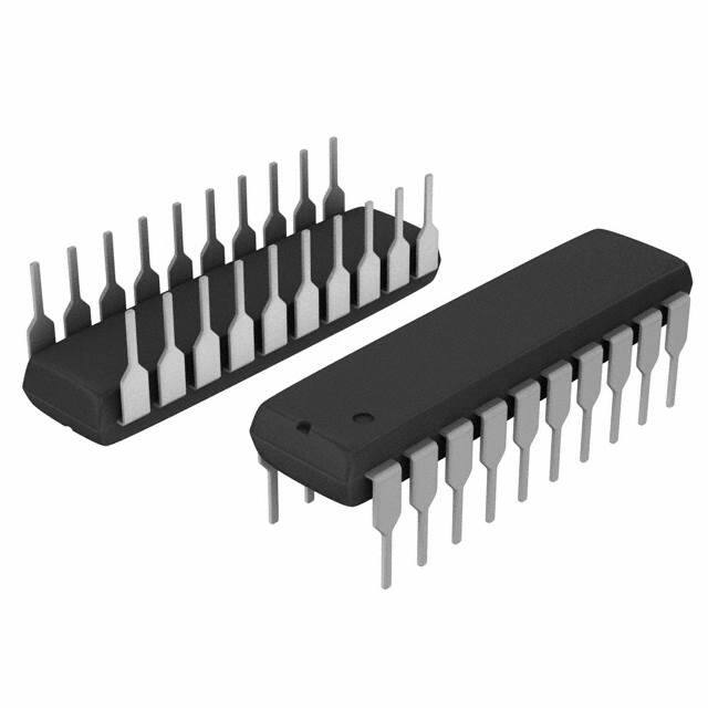


 工商网监
湘ICP备2023018690号
工商网监
湘ICP备2023018690号
