®
SMP75-8
TRISIL™ FOR TELECOM EQUIPMENT PROTECTION
FEATURES
■ ■ ■ ■ ■
Bidirectional crowbar protection Voltage: 8V Low leakage current : IR = 2µA max Holding current: IH = 150 mA min Repetitive peak pulse current : IPP = 75 A (10/1000µs)
MAIN APPLICATIONS Any sensitive equipment requiring protection against lightning strikes and power crossing:
■
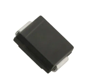
SMB (JEDEC DO-214AA)
Ethernet, T1/E1 Table 1: Order Code Part Number SMP75-8
DESCRIPTION The SMP75-8 is a very low voltage transient surge arrestor especially designed to protect sensitive telecommunication equipment against lightning strikes and other transients. Its low voltage makes it suitable to protect low voltage transformer in T1/ E1, ethernet links without saturation of the transformer. BENEFITS Trisils are not subject to ageing and provide a fail safe mode in short circuit for a better protection. They are used to help equipment to meet main standards such as UL1950, IEC950 / CSA C22.2 and UL1459. They have UL94 V0 approved resin. SMB package is JEDEC registered (DO-214AA). Trisils comply with the following standards GR1089 Core, ITU-T-K20/K21, VDE0433, VDE0878, IEC61000-4-5 and FCC part 68.
Marking L08
Figure 1: Schematic Diagram
TM: TRISIL is a trademark of STMicroelectronics.
January 2006
REV. 4
1/8
�SMP75-8
Table 2: In compliances with the following standards STANDARD GR-1089 Core First level GR-1089 Core Second level GR-1089 Core Intra-building ITU-T-K20/K21 ITU-T-K20 (IEC61000-4-2) VDE0433 VDE0878 IEC61000-4-5 FCC Part 68, lightning surge type A FCC Part 68, lightning surge type B Peak Surge Voltage (V) 2500 1000 5000 1500 6000 1500 8000 15000 4000 2000 4000 2000 4000 4000 1500 800 1000 Waveform Voltage 2/10 µs 10/1000 µs 2/10 µs 2/10 µs 10/700 µs 1/60 ns 10/700 µs 1.2/50 µs 10/700 µs 1.2/50 µs 10/160 µs 10/560 µs 9/720 µs Required peak current (A) 500 100 500 100 150 37.5 Current waveform 2/10 µs 10/1000 µs 2/10 µs 2/10 µs 5/310 µs Minimum serial resistor to meet standard (Ω) 5 3.3 10 0 10 0 0 0 0 0 0 0 0 0 2.5 0 0
ESD contact discharge ESD air discharge 100 50 100 50 100 100 200 100 25 5/310 µs 1/20 µs 5/310 µs 8/20 µs 10/160 µs 10/560 µs 5/320 µs
Table 3: Absolute Ratings (Tamb = 25°C) Symbol Parameter 10/1000 µs 8/20 µs 10/560 µs 5/310 µs 10/160 µs 1/20 µs 2/10 µs 8/20 µs t = 0.2 s t=1s t=2s t = 15 mn t = 16.6 ms t = 20 ms Value 75 250 100 120 150 250 250 5 14 8 6.5 2 12 12.2 -55 to 150 150 260 Unit
IPP
Repetitive peak pulse current
A
IFS ITSM
Fail-safe mode : maximum current (note 1) Non repetitive surge peak on-state current (sinusoidal)
kA A
I2t Tstg Tj TL
I2t value for fusing Storage temperature range Maximum junction temperature Maximum lead temperature for soldering during 10 s.
A2s °C °C
Note 1: in fail safe mode, the device acts as a short circuit
2/8
�SMP75-8
Table 4: Thermal Resistances Symbol Parameter Rth(j-a) Junction to ambient (with recommended footprint) Rth(j-l) Junction to leads Value 100 20 Unit °C/W °C/W
Table 5: Electrical Characteristics (Tamb = 25°C) Symbol VRM VBR VBO IRM IPP IBO IH VR IR C Parameter Stand-off voltage Breakdown voltage Breakover voltage Leakage current Peak pulse current Breakover current Holding current Continuous reverse voltage Leakage current at VR Capacitance Dynamic VBO max. note 2 V 8 V 20 V 15 Static VBO @ IBO max. max.
IRM @ VRM Types µA SMP75-8
Note 1: Note 2: Note 3: Note 4: Note 5:
IR @ VR max. note1
IH typ. note 4 mA 50
C max. note 5 pF 60
max. V 6
note 3 mA 800
µA 5
2
IR measured at VR guarantee VBR min ≥ VR see functional test circuit 1 see test circuit 2 see functional holding current test circuit 3 VR = 2V bias, VRMS=1V, F=1MHz
Figure 2: Pulse waveform
Figure 3: Non repetitive surge peak on-state current versus overload duration
ITSM(A)
Repetitive peak pulse current tr = rise time (µs) tp = pulse duration time (µs)
% I PP 100
50 45 40 35 30
F=50Hz Tj initial = 25°C
50
25 20 15
0 tr tp
10
t
5
t(s)
0 1E-2 1E-1 1E+0 1E+1 1E+2 1E+3
3/8
�SMP75-8
Figure 4: On-state voltage versus on-state current (typical values)
IT(A)
100
Tj=25°C
Figure 5: Relative variation of holding current versus junction temperature
IH[Tj] / IH[Tj=25°C]
2.0 1.8 1.6 1.4 1.2 1.0 0.8 0.6 0.4
VT(V)
10 0 1 2 3 4 5 6 7 8
0.2 0.0 -40 -30 -20 -10 0 10 20 30
Tj(°C)
40 50 60 70 80 90 100 110 120 130
Figure 6: Relative variation of breakover voltage versus junction temperature
VBO[Tj] / VBO[Tj=25°C]
1.08 1.07 1.06 1.05 1.04 1.03 1.02 1.01 1.00 0.99 0.98 0.97 0.96 0.95 0.94 -40 -30 -20 -10 0 10 20 30 40 50 60 70 80 90 100 110 120 130
Figure 7: Relative variation of leakage current versus reverse voltage applied (typical values)
10000
IR[Tj] / IR[Tj=25°C]
1000
100
10
Tj(°C)
1 25 50
Tj(°C)
75 100 125
Figure 8: Variation of thermal impedance junction to ambient versus pulse duration (Printed circuit board FR4, SCu=35µm, recommended pad layout)
Zth(j-a)/Rth(j-a)
1.0 0.9 0.8 0.7 0.6 0.5 0.4 0.3 0.2 0.1 0.0 1.E-02 1.E-01 1.E+00 1.E+01 1.E+02 1.E+03
Figure 9: Relative variation of junction capacitance versus reverse voltage applied (typical values)
C [VR] / C [VR=2V]
1.2 1.1 1.0 0.9 0.8 0.7 0.6 0.5 0.4 0.3 0.2
F =1MHz VOSC = 1VRMS Tj = 25°C
tp(s)
0.1 0.0 1
VR(V)
10
4/8
�SMP75-8
Figure 10: Test circuit 1 for dynamic IBO and VBO parameters
100 V / µs, di /dt < 10 A / µs, Ipp = 75 A
2Ω
45 Ω 66 Ω 470 Ω
83 Ω 0.36 nF
46 µH
U
10 µF
KeyTek 'System 2' generator with PN246I module
1 kV / µs, di /dt < 10 A / µs, Ipp = 10 A
26 µH
250 Ω 12 Ω
47 Ω
46 µH
U
60 µF
KeyTek 'System 2' generator with PN246I module
Figure 11: Test circuit 2 for IBO and VBO parameters
K
ton = 20ms
R1 = 140Ω R2 = 240Ω
220V 50Hz Vout
DUT
VBO measurement
1/4 IBO measurement
TEST PROCEDURE
Pulse test duration (tp = 20ms): ● for Bidirectional devices = Switch K is closed ● for Unidirectional devices = Switch K is open VOUT selection: ● Device with VBO < 200V ➔ VOUT = 250 VRMS, R1 = 140Ω ● Device with VBO ≥ 200V ➔ VOUT = 480 VRMS, R2 = 240Ω
5/8
�SMP75-8
Figure 12: Test circuit 3 for dynamic IH parameter
R
Surge generator
VBAT = - 48 V
D.U.T
This is a GO-NOGO test which allows to confirm the holding current (IH) level in a functional test circuit.
TEST PROCEDURE
1/ Adjust the current level at the IH value by short circuiting the AK of the D.U.T. 2/ Fire the D.U.T. with a surge current ➔ IPP = 10A, 10/1000µs. 3/ The D.U.T. will come back off-state within 50ms maximum.
Figure 12: Ordering Information Scheme
SMP
Trisil Surface Mount Repetitive Peak Pulse Current 75 = 75A Voltage 8 = 8V
75
-
8
6/8
�SMP75-8
Figure 13: SMB Package Mechanical data
E1
REF.
D
E
A1
C L
A2
b
A1 A2 b c E E1 D L
DIMENSIONS Millimeters Inches Min. Max. Min. Max. 1.90 2.45 0.075 0.096 0.05 0.20 0.002 0.008 1.95 2.20 0.077 0.087 0.15 0.41 0.006 0.016 5.10 5.60 0.201 0.220 4.05 4.60 0.159 0.181 3.30 3.95 0.130 0.156 0.75 1.60 0.030 0.063
Figure 14: Foot Print Dimensions (in millimeters)
2.3
1.52
2.75
1.52
In order to meet environmental requirements, ST offers these devices in ECOPACK® packages. These packages have a Lead-free second level interconnect . The category of second level interconnect is marked on the package and on the inner box label, in compliance with JEDEC Standard JESD97. The maximum ratings related to soldering conditions are also marked on the inner box label. ECOPACK is an ST trademark. ECOPACK specifications are available at: www.st.com. Table 6: Ordering Information Part Number SMP75-8 Marking L08 Package SMB Weight 0.11 g Base qty 2500 Delivery mode Tape & reel
Table 7: Revision History Date 19-July-2005 02-Jan-2006 Revision 3 4 Previous issue Added ECOPACK statement and changed page layout. Minor updates to technical values in Tables 2, 3, and 5. Description of Changes
7/8
�SMP75-8
Information furnished is believed to be accurate and reliable. However, STMicroelectronics assumes no responsibility for the consequences of use of such information nor for any infringement of patents or other rights of third parties which may result from its use. No license is granted by implication or otherwise under any patent or patent rights of STMicroelectronics. Specifications mentioned in this publication are subject to change without notice. This publication supersedes and replaces all information previously supplied. STMicroelectronics products are not authorized for use as critical components in life support devices or systems without express written approval of STMicroelectronics. The ST logo is a registered trademark of STMicroelectronics. All other names are the property of their respective owners © 2006 STMicroelectronics - All rights reserved STMicroelectronics group of compagnies Australia - Belgium - Brazil - Canada - China - Czech Republic - Finland - France - Germany - Hong Kong - India - Israel - Italy - Japan Malaysia - Malta - Morocco - Singapore - Spain - Sweden - Switzerland - United Kingdom - United States of America www.st.com
8/8
�
很抱歉,暂时无法提供与“SMP75-8”相匹配的价格&库存,您可以联系我们找货
免费人工找货- 国内价格
- 1+2.47123
- 30+2.38602
- 100+2.21559
- 500+2.04516
- 1000+1.95994
- 国内价格 香港价格
- 2500+1.296042500+0.15723
- 5000+1.289995000+0.15649
- 7500+1.289967500+0.15649
- 12500+1.2899312500+0.15649
- 25000+1.2899125000+0.15648


 工商网监
湘ICP备2023018690号
工商网监
湘ICP备2023018690号
