STGB7NC60HD,
STGF7NC60HD, STGP7NC60HD
N-channel 14 A, 600 V, very fast IGBT with Ultrafast diode
Datasheet − production data
Features
TAB
■
Low on-voltage drop (VCE(sat))
■
Off losses include tail current
■
Losses include diode recovery energy
■
High frequency operation up to 70 kHz
■
Very soft ultra fast recovery anti parallel diode
TAB
3
1
3
12
D²PAK (TO-263)
I²PAK (TO-262)
TAB
Applications
■
3
High frequency inverters
3
■
SMPS and PFC in both hard switch and
resonant topologies
■
Motor drivers
1
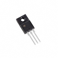
TO-220
Figure 1.
Description
1
2
2
TO-220FP
Internal schematic diagram
C (2, TAB)
These devices are very fast IGBT developed
using advanced PowerMESH™ technology. This
process guarantees an excellent trade-off
between switching performance and low on-state
behavior. These devices are well-suited for
resonant or soft-switching applications.
G (1)
E (3)
Table 1.
Device summary
Order codes
Markings
STGB7NC60HD-1
Packages
Packaging
I²PAK (TO-262)
Tube
D²PAK (TO-263)
Tape and reel
GB7NC60HD
STGB7NC60HDT4
STGF7NC60HD
GF7NC60HD
TO-220FP
Tube
STGP7NC60HD
GP7NC60HD
TO-220
Tube
June 2012
This is information on a product in full production.
Doc ID 10042 Rev 10
1/22
www.st.com
22
�Contents
STGB7NC60HD, STGF7NC60HD, STGP7NC60HD
Contents
1
Electrical ratings . . . . . . . . . . . . . . . . . . . . . . . . . . . . . . . . . . . . . . . . . . . . 3
2
Electrical characteristics . . . . . . . . . . . . . . . . . . . . . . . . . . . . . . . . . . . . . 4
2.1
Electrical characteristics (curves) . . . . . . . . . . . . . . . . . . . . . . . . . . . . . . . 6
2.2
Operating frequency . . . . . . . . . . . . . . . . . . . . . . . . . . . . . . . . . . . . . . . . . . 9
3
Test circuits . . . . . . . . . . . . . . . . . . . . . . . . . . . . . . . . . . . . . . . . . . . . . . . 10
4
Package mechanical data . . . . . . . . . . . . . . . . . . . . . . . . . . . . . . . . . . . . 11
5
Packaging mechanical data . . . . . . . . . . . . . . . . . . . . . . . . . . . . . . . . . . 19
6
Revision history . . . . . . . . . . . . . . . . . . . . . . . . . . . . . . . . . . . . . . . . . . . 21
2/22
Doc ID 10042 Rev 10
�STGB7NC60HD, STGF7NC60HD, STGP7NC60HD
1
Electrical ratings
Electrical ratings
Table 2.
Absolute maximum ratings
Value
Symbol
Parameter
I2PAK, D2PAK,
TO-220
Unit
TO-220FP
VCES
Collector-emitter voltage (VGS = 0)
600
V
VECR
Emitter-collector voltage
20
V
VGE
Gate-emitter voltage
±20
V
IC
IC
ICM
(2)
IF
PTOT
Collector current (continuous) at TC = 25 °C (1)
Collector current (continuous) at TC = 100 °C
(1)
10
A
14
6
A
Collector current (pulsed)
50
A
Diode RMS forward current at TC = 25°C
20
A
Total dissipation at TC = 25°C
Derating factor
VISO
Insulation withstand voltage A.C. (t = 1 sec;
TC = 25°C)
Tstg
Storage temperature
Tj
25
80
25
W
0.64
0.20
W/°C
--
2500
V
– 55 to 150
°C
Operating junction temperature
1. Calculated according to the iterative formula:
Tj ( max ) – T C
I C ( TC ) = ------------------------------------------------------------------------------------------------------R thj – c × VCE ( sat ) ( max ) ( T j ( max ), IC ( T C ) )
2. Pulse width limited by maximum junction temperature and turn-off within RBSOA.
Table 3.
Thermal data
Value
Symbol
Parameter
RthJC
Thermal resistance junction-case
RthJA
Thermal resistance junction-ambient
Doc ID 10042 Rev 10
Unit
I2PAK, D2PAK,
TO-220
TO-220FP
1.56
5.0
62.5
°C/W
°C/W
3/22
�Electrical characteristics
2
STGB7NC60HD, STGF7NC60HD, STGP7NC60HD
Electrical characteristics
TCASE = 25°C unless otherwise specified.
Table 4.
Symbol
Electrical characteristics
Parameter
Test conditions
Collector-emitter
breakdown voltage
IC = 1 mA, VGE = 0
ICES
Collector cut-off current
(VGE = 0)
VCE = 600 V
VCE = 600 V, TC = 125 °C
IGES
Gate-emitter leakage
current (VCE = 0)
VGE = ± 20 V
VGE(th)
Gate threshold voltage
VCE = VGE, IC = 250 µA
VCE(sat)
Collector-emitter
saturation voltage
VGE = 15V, IC = 7 A
VGE = 15V, IC = 7 A, TC= 125°C
V(BR)CES
Table 5.
Symbol
Min.
Typ.
Max.
600
Unit
V
3.75
1.85
1.7
10
1
µA
mA
±100
nA
5.75
V
2.5
V
V
Max.
Unit
Dynamic
Parameter
Test conditions
gfs (1)
Forward
transconductance
Cies
Input capacitance
Coes
Output capacitance
Cres
Reverse transfer
capacitance
Qg
Qge
Qgc
Total gate charge
Gate-emitter charge
Gate-collector charge
VCE = 390 V, IC = 7 A,
VGE = 15 V
ICL
Turn-off SOA minimum
current
Vclamp = 480 V , Tj =150°C
RG = 10 Ω, VGE = 15 V
Min.
VCE = 15 V , IC = 7 A
VCE = 25 V, f = 1 MHz,
VGE = 0
Typ.
4.30
S
720
pF
81
pF
17
pF
35
7
16
48
50
nC
nC
nC
A
1. Pulsed: Pulse duration= 300 µs, duty cycle 1.5%
Table 6.
Symbol
4/22
Switching on
Parameter
Test conditions
td(on)
tr
(di/dt)on
Turn-on delay time
Current rise time
Turn-on current slope
VCC = 390 V, IC = 7 A
RG = 10 Ω, VGE = 15V
(see Figure 21)
td(on)
tr
(di/dt)on
Turn-on delay time
Current rise time
Turn-on current slope
VCC = 390 V, IC = 7 A
RG = 10 Ω, VGE = 15V,
Tj = 125°C (see Figure 21)
Min.
Typ.
18.5
8.5
1060
-
Doc ID 10042 Rev 10
Max.
Unit
ns
ns
A/µs
18.5
7
1000
ns
ns
A/µs
�STGB7NC60HD, STGF7NC60HD, STGP7NC60HD
Table 7.
Symbol
tr(Voff)
td(off)
tf
Switching off
Parameter
Test conditions
Turn-off delay time
Current fall time
72
ns
ns
-
VCC = 390 V, IC = 7 A,
RG = 10 Ω , VGE = 15 V
Tj = 125 °C
Current fall time
Unit
ns
60
Turn-off delay time
Eon (1)
Max.
27
-
td(off)
Symbol
Typ.
VCC = 390 V, IC = 7 A,
RG = 10 Ω , VGE = 15 V
Off voltage rise time
Table 8.
Min.
Off voltage rise time
tr(Voff)
tf
Electrical characteristics
56
ns
116
ns
105
ns
Switching energy
Parameter
Test conditions
(2)
Eoff
Ets
Turn-on switching losses
Turn-off switching loss
Total switching loss
VCC = 390 V, IC = 7 A
RG = 10 Ω, VGE = 15 V,
Eon (1)
Eoff (2)
Ets
Turn-on switching losses
Turn-off switching loss
Total switching loss
VCC = 390 V, IC = 7 A
RG = 10 Ω, VGE = 15 V,
Tj = 125°C
Min.
Typ.
Max
Unit
95
115
210
125
150
275
µJ
µJ
µJ
140
215
355
µJ
µJ
µJ
1. Eon is the turn-on losses when a typical diode is used in the test circuit. If the IGBT is offered in a package
with a co-pack diode, the co-pack diode is used as external diode. IGBTs and diode are at the same
temperature (25°C and 125°C).
2. Turn-off losses include also the tail of the collector current.
Table 9.
Symbol
Vf
Collector-emitter diode
Parameter
Forward on-voltage
trr
ta
Qrr
Irrm
S
Reverse recovery time
trr
ta
Qrr
Irrm
S
Reverse recovery time
Reverse recovery charge
Reverse recovery current
Softness factor of the diode
Reverse recovery charge
Reverse recovery current
Softness factor of the diode
Test conditions
Min.
Typ.
Max.
Unit
If = 3.5 A
If = 3.5 A, Tj = 125 °C
1.3
1.1
1.9
V
V
If = 7 A, VR = 40 V,
di/dt = 100 A/µs
37
22
40
2.1
0.68
ns
ns
nC
A
61
34
98
3.2
0.79
ns
ns
nC
A
-
If = 7 A, VR = 40 V,
Tj = 125 °C, di/dt = 100 A/µs
Doc ID 10042 Rev 10
5/22
�Electrical characteristics
STGB7NC60HD, STGF7NC60HD, STGP7NC60HD
2.1
Electrical characteristics (curves)
Figure 2.
Output characteristics
Figure 3.
Transfer characteristics
Figure 4.
Transconductance
Figure 5.
Collector-emitter on voltage vs.
temperature
Figure 6.
Collector-emitter on voltage vs.
collector current
Figure 7.
Normalized gate threshold vs.
temperature
6/22
Doc ID 10042 Rev 10
�STGB7NC60HD, STGF7NC60HD, STGP7NC60HD
Figure 8.
Normalized breakdown voltage vs
temperature
Electrical characteristics
Figure 9.
Gate charge vs. gate-emitter
voltage
Figure 10. Capacitance variations
Figure 11. Total switching losses vs.
temperature
Figure 12. Total switching losses vs. gate
resistance
Figure 13. Total switching losses vs collector
current
Doc ID 10042 Rev 10
7/22
�Electrical characteristics
STGB7NC60HD, STGF7NC60HD, STGP7NC60HD
Figure 14. Emitter-collector diode
characteristics
Figure 15. Turn-off SOA
Figure 16. Thermal impedance for I2PAK,
D2PAK and TO-220
Figure 17. Thermal impedance for TO-220FP
8/22
Doc ID 10042 Rev 10
�STGB7NC60HD, STGF7NC60HD, STGP7NC60HD
2.2
Electrical characteristics
Operating frequency
Figure 18. IC vs. frequency
For a fast IGBT suitable for high frequency applications, the typical collector current vs.
maximum operating frequency curve is reported. That frequency is defined as follows:
Equation 1
fMAX = (PD - PC) / (EON + EOFF)
The maximum power dissipation is limited by maximum junction to case thermal resistance:
Equation 2
PD = ΔT / RTHJ-C
considering ΔT = TJ - TC = 125 °C- 75 °C = 50°C
The conduction losses are:
Equation 3
PC = IC * VCE(SAT) * δ
with 50% of duty cycle, VCE(sat) typical value TC = 125°C.
Power dissipation during ON & OFF commutations is due to the switching frequency:
Equation 4
PSW = (EON + EOFF) * freq.
Typical values TC = 125°C for switching losses are used (test conditions: VCE = 390 V,
VGE = 15 V, RG = 3.3 Ω). Furthermore, diode recovery energy is included in the EON, while
the tail of the collector current is included in the EOFF measurements.
Doc ID 10042 Rev 10
9/22
�Test circuits
3
STGB7NC60HD, STGF7NC60HD, STGP7NC60HD
Test circuits
Figure 19. Test circuit for inductive load
switching
Figure 20. Gate charge test circuit
AM01505v1
Figure 21. Switching waveform
Figure 22. Diode recovery time waveform
VG
IF
trr
90%
VCE
Qrr
di/dt
90%
10%
ta
tb
10%
Tr(Voff)
t
Tcross
90%
IRRM
IRRM
IC
10%
Td(off)
Td(on)
Tr(Ion)
Ton
Tf
Toff
VF
dv/dt
AM01506v1
10/22
Doc ID 10042 Rev 10
AM01507v1
�STGB7NC60HD, STGF7NC60HD, STGP7NC60HD
4
Package mechanical data
Package mechanical data
In order to meet environmental requirements, ST offers these devices in different grades of
ECOPACK® packages, depending on their level of environmental compliance. ECOPACK®
specifications, grade definitions and product status are available at: www.st.com. ECOPACK
is an ST trademark.
Table 10.
I²PAK (TO-262) mechanical data
mm.
Dim.
Min.
Typ.
Max.
A
4.40
4.60
A1
2.40
2.72
b
0.61
0.88
b1
1.14
1.70
c
0.49
0.70
c2
1.23
1.32
D
8.95
9.35
e
2.40
2.70
e1
4.95
5.15
E
10
10.40
L
13
14
L1
3.50
3.93
L2
1.27
1.40
Doc ID 10042 Rev 10
11/22
�Package mechanical data
STGB7NC60HD, STGF7NC60HD, STGP7NC60HD
Figure 23. I²PAK (TO-262) drawing
0004982_Rev_H
12/22
Doc ID 10042 Rev 10
�STGB7NC60HD, STGF7NC60HD, STGP7NC60HD
Table 11.
Package mechanical data
D²PAK (TO-263) mechanical data
mm
Dim.
Min.
Typ.
Max.
A
4.40
4.60
A1
0.03
0.23
b
0.70
0.93
b2
1.14
1.70
c
0.45
0.60
c2
1.23
1.36
D
8.95
9.35
D1
7.50
E
10
E1
8.50
10.40
e
2.54
e1
4.88
5.28
H
15
15.85
J1
2.49
2.69
L
2.29
2.79
L1
1.27
1.40
L2
1.30
1.75
R
V2
0.4
0°
8°
Doc ID 10042 Rev 10
13/22
�Package mechanical data
STGB7NC60HD, STGF7NC60HD, STGP7NC60HD
Figure 24. D²PAK (TO-263) drawing
0079457_T
Figure 25. D²PAK footprint(a)
16.90
12.20
5.08
1.60
3.50
9.75
a. All dimensions are in millimeters
14/22
Doc ID 10042 Rev 10
Footprint
�STGB7NC60HD, STGF7NC60HD, STGP7NC60HD
Table 12.
Package mechanical data
TO-220FP mechanical data
mm
Dim.
Min.
Typ.
Max.
A
4.4
4.6
B
2.5
2.7
D
2.5
2.75
E
0.45
0.7
F
0.75
1
F1
1.15
1.70
F2
1.15
1.70
G
4.95
5.2
G1
2.4
2.7
H
10
10.4
L2
16
L3
28.6
30.6
L4
9.8
10.6
L5
2.9
3.6
L6
15.9
16.4
L7
9
9.3
Dia
3
3.2
Doc ID 10042 Rev 10
15/22
�Package mechanical data
STGB7NC60HD, STGF7NC60HD, STGP7NC60HD
Figure 26. TO-220FP drawing
7012510_Rev_K_B
16/22
Doc ID 10042 Rev 10
�STGB7NC60HD, STGF7NC60HD, STGP7NC60HD
Table 13.
Package mechanical data
TO-220 type A mechanical data
mm
Dim.
Min.
Typ.
Max.
A
4.40
4.60
b
0.61
0.88
b1
1.14
1.70
c
0.48
0.70
D
15.25
15.75
D1
1.27
E
10
10.40
e
2.40
2.70
e1
4.95
5.15
F
1.23
1.32
H1
6.20
6.60
J1
2.40
2.72
L
13
14
L1
3.50
3.93
L20
16.40
L30
28.90
∅P
3.75
3.85
Q
2.65
2.95
Doc ID 10042 Rev 10
17/22
�Package mechanical data
STGB7NC60HD, STGF7NC60HD, STGP7NC60HD
Figure 27. TO-220 type A drawing
0015988_typeA_Rev_S
18/22
Doc ID 10042 Rev 10
�STGB7NC60HD, STGF7NC60HD, STGP7NC60HD
5
Packaging mechanical data
Packaging mechanical data
Table 14.
D²PAK (TO-263) tape and reel mechanical data
Tape
Reel
mm
mm
Dim.
Dim.
Min.
Max.
Min.
A0
10.5
10.7
A
B0
15.7
15.9
B
1.5
D
1.5
1.6
C
12.8
D1
1.59
1.61
D
20.2
E
1.65
1.85
G
24.4
F
11.4
11.6
N
100
K0
4.8
5.0
T
P0
3.9
4.1
P1
11.9
12.1
Base qty
1000
P2
1.9
2.1
Bulk qty
1000
R
50
T
0.25
0.35
W
23.7
24.3
Doc ID 10042 Rev 10
Max.
330
13.2
26.4
30.4
19/22
�Packaging mechanical data
STGB7NC60HD, STGF7NC60HD, STGP7NC60HD
Figure 28. Tape
10 pitches cumulative
tolerance on tape +/- 0.2 mm
T
P0
Top cover
tape
P2
D
E
F
W
K0
B0
A0
P1
D1
User direction of feed
R
Bending radius
User direction of feed
AM08852v2
Figure 29. Reel
T
REEL DIMENSIONS
40mm min.
Access hole
At sl ot location
B
D
C
N
A
Full radius
Tape slot
in core for
tape start 25 mm min.
width
G measured at hub
AM08851v2
20/22
Doc ID 10042 Rev 10
�STGB7NC60HD, STGF7NC60HD, STGP7NC60HD
6
Revision history
Revision history
Table 15.
Document revision history
Date
Revision
Changes
07-Jun-2004
4
Stylesheet update. No content change.
19-Aug-2004
5
Complete version
17-Sep-2004
6
Figure 14 has been added
09-Nov-2004
7
Final datasheet
19-Jan-2005
8
Datasheet updated
09-Jun-2005
9
Modified title
27-Jun-2012
10
Inserted commercial type STGB7NC60HD.
Minor text changes.
Doc ID 10042 Rev 10
21/22
�STGB7NC60HD, STGF7NC60HD, STGP7NC60HD
Please Read Carefully:
Information in this document is provided solely in connection with ST products. STMicroelectronics NV and its subsidiaries (“ST”) reserve the
right to make changes, corrections, modifications or improvements, to this document, and the products and services described herein at any
time, without notice.
All ST products are sold pursuant to ST’s terms and conditions of sale.
Purchasers are solely responsible for the choice, selection and use of the ST products and services described herein, and ST assumes no
liability whatsoever relating to the choice, selection or use of the ST products and services described herein.
No license, express or implied, by estoppel or otherwise, to any intellectual property rights is granted under this document. If any part of this
document refers to any third party products or services it shall not be deemed a license grant by ST for the use of such third party products
or services, or any intellectual property contained therein or considered as a warranty covering the use in any manner whatsoever of such
third party products or services or any intellectual property contained therein.
UNLESS OTHERWISE SET FORTH IN ST’S TERMS AND CONDITIONS OF SALE ST DISCLAIMS ANY EXPRESS OR IMPLIED
WARRANTY WITH RESPECT TO THE USE AND/OR SALE OF ST PRODUCTS INCLUDING WITHOUT LIMITATION IMPLIED
WARRANTIES OF MERCHANTABILITY, FITNESS FOR A PARTICULAR PURPOSE (AND THEIR EQUIVALENTS UNDER THE LAWS
OF ANY JURISDICTION), OR INFRINGEMENT OF ANY PATENT, COPYRIGHT OR OTHER INTELLECTUAL PROPERTY RIGHT.
UNLESS EXPRESSLY APPROVED IN WRITING BY TWO AUTHORIZED ST REPRESENTATIVES, ST PRODUCTS ARE NOT
RECOMMENDED, AUTHORIZED OR WARRANTED FOR USE IN MILITARY, AIR CRAFT, SPACE, LIFE SAVING, OR LIFE SUSTAINING
APPLICATIONS, NOR IN PRODUCTS OR SYSTEMS WHERE FAILURE OR MALFUNCTION MAY RESULT IN PERSONAL INJURY,
DEATH, OR SEVERE PROPERTY OR ENVIRONMENTAL DAMAGE. ST PRODUCTS WHICH ARE NOT SPECIFIED AS "AUTOMOTIVE
GRADE" MAY ONLY BE USED IN AUTOMOTIVE APPLICATIONS AT USER’S OWN RISK.
Resale of ST products with provisions different from the statements and/or technical features set forth in this document shall immediately void
any warranty granted by ST for the ST product or service described herein and shall not create or extend in any manner whatsoever, any
liability of ST.
ST and the ST logo are trademarks or registered trademarks of ST in various countries.
Information in this document supersedes and replaces all information previously supplied.
The ST logo is a registered trademark of STMicroelectronics. All other names are the property of their respective owners.
© 2012 STMicroelectronics - All rights reserved
STMicroelectronics group of companies
Australia - Belgium - Brazil - Canada - China - Czech Republic - Finland - France - Germany - Hong Kong - India - Israel - Italy - Japan Malaysia - Malta - Morocco - Philippines - Singapore - Spain - Sweden - Switzerland - United Kingdom - United States of America
www.st.com
22/22
Doc ID 10042 Rev 10
�


 工商网监
湘ICP备2023018690号
工商网监
湘ICP备2023018690号

