DG9421E, DG9422E
www.vishay.com
Vishay Siliconix
1.7 , Low On Resistance, +12 V, +5 V, +3 V, ± 5 V,
SPST Switches
DESCRIPTION
FEATURES
The
DG9421E
and
DG9422E
are
monolithic
single-pole-single-throw (SPST) analog switches. The
DG9421E has a normally closed function. The DG9422E has
a normally open function.
• 3 V to 16 V single supply or ± 3 thru ± 8 V dual
supply operation
Available
• Low on resistance: 1.7 typical at 12 V
Available
• 2.4 V logic compatible for control
• Bi-directional rail to rail signal switching
• Fast switching speed
• High bandwidth: 161 MHz
• Control logic input can be over V+
• Material categorization: for definitions of compliance
please see www.vishay.com/doc?99912
Processed with high density BiCMOS technology, the parts
achieve low resistance, fast switching speed, low power
dissipation, high -3dB bandwidth, and low voltage logic
control threshold.
The DG9421E and DG9422E operate on single and dual
supplies. Single supply voltage ranges from +3 V to +16 V
while dual supply operation is recommended with ± 3 V to
± 8 V. Each switch conducts equally well in both direction
when on, and blocks input voltages up to the supply levels
when off.
The low and flat on resistance over the full input signal
voltage range brings excellent linearity, reduces insertion
loss and signal distortion, makes them ideal for data
acquisition and programmable gain control applications.
These switch characters also make them ideal fit for audio
signal switch and reed relay replacement.
Operation temperature is specified from -40 °C to +85 °C.
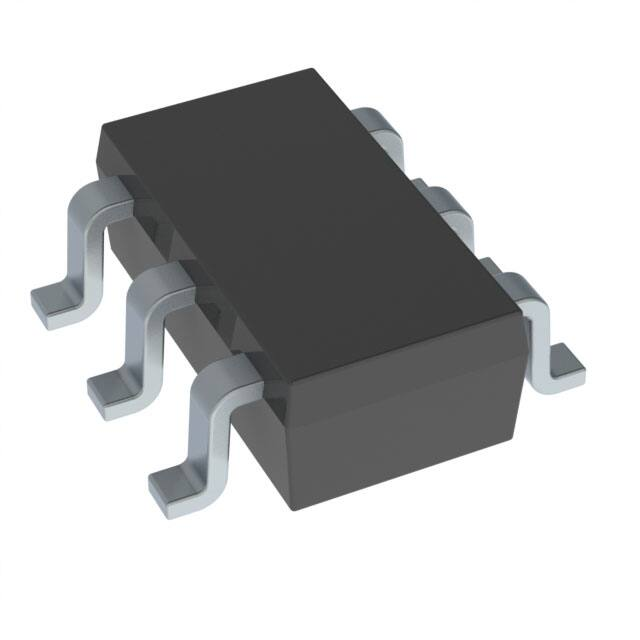
The DG9421E and DG9422E are available in 6 lead TSSOP
packages.
BENEFITS
•
•
•
•
Wide operation voltage range
Low signal errors and distortion
Fast switching time
Simple interfacing
Note
* This datasheet provides information about parts that are
RoHS-compliant and / or parts that are non RoHS-compliant. For
example, parts with lead (Pb) terminations are not RoHS-compliant.
Please see the information / tables in this datasheet for details
APPLICATIONS
•
•
•
•
•
•
•
•
•
•
Automatic test equipment
Data acquisition systems
Meters and instruments
Medical and healthcare systems
Communication systems
Audio and video signal routing
Relay replacement
Battery powered systems
Computer peripherals
Audio and video signal routing
FUNCTIONAL BLOCK DIAGRAM AND PIN CONFIGURATION
TSOP-6
V+
1
6
IN
COM
2
5
NC
V-
4
3
GND
Top View
Device Marking:
DG9421EDV = 4Mxxx
TRUTH TABLE
LOGIC
DG9421E
DG9422E
0
On
Off
1
Off
On
Notes
• Logic “0” 0.8 V
• Logic “1” 2.4 V
• Switches shown for logic “0” input
TSOP-6
V+
1
6
IN
COM
2
5
NO
V-
3
4
GND
Top View
Device Marking:
DG9422EDV = 4Nxxx
S18-0592-Rev. A, 25-Jun-2018
ORDERING INFORMATION
TEMP. RANGE
PACKAGE
-40 °C to +85 °C
6-pin TSOP
PART NUMBER
DG9421EDV-T1-GE3
DG9422EDV-T1-GE3
Document Number: 75411
1
For technical questions, contact: powerictechsupport@vishay.com
THIS DOCUMENT IS SUBJECT TO CHANGE WITHOUT NOTICE. THE PRODUCTS DESCRIBED HEREIN AND THIS DOCUMENT
ARE SUBJECT TO SPECIFIC DISCLAIMERS, SET FORTH AT www.vishay.com/doc?91000
�DG9421E, DG9422E
www.vishay.com
Vishay Siliconix
ABSOLUTE MAXIMUM RATINGS
PARAMETER
V+ reference to VIN
V+ reference to GND
GND reference to V-
LIMIT
-0.3 to +18
-0.3 to +18
-0.3 to +18
-0.3 to +18
(V-) - 0.3 V to (V+) + 0.3 V
or 50 mA, whichever occurs first
50
100
-65 to +150
570
2000
2000
300
COM, NC, NO a
UNIT
V
-
Continuous current (any terminal)
mA
Peak current, NO, NC or COM (pulsed at 1 ms, 10 % duty cycle)
Storage temperature
°C
6-pin TSOP c
mW
Power dissipation (packages) b
ESD / HBM
JS-001
V
ESD / CDM
JS-002
Latch up
per JEDEC78
mA
Notes
a. Signals on NO, NC, COM exceeding V+ or V- will be clamped by internal diodes. Limit forward diode current to maximum current ratings
b. All leads welded or soldered to PC board
c. Derate 7 mW/°C above 25 °C
Stresses beyond those listed under “Absolute Maximum Ratings” may cause permanent damage to the device. These are stress ratings only, and functional operation
of the device at these or any other conditions beyond those indicated in the operational sections of the specifications is not implied. Exposure to absolute maximum
rating conditions for extended periods may affect device reliability.
SPECIFICATIONS
a
(Single supply 12 V)
PARAMETER
Analog Switch
Analog signal range a
Drain-source
on-resistance
Switch off
leakage current g
Channel-on
leakage current g
Digital Control
Input current, VIN low
Input current, VIN high
Dynamic Characteristics
Turn-on time e
Turn-off time e
Charge injection e
Bandwidth e
Off-isolation e
Source off capacitance e
Drain off capacitance e
Channel on capacitance e
Power Supplies
SYMBOL
VANALOG
RDS(on)
VCOM = 1 V / 11 V, VNO/NC = 11 V / 1 V
ICOM(off)
ICOM(on)
VNO/NC = VCOM = 11 V / 1 V
IIL
IIH
VIN under test = 0.8 V
VIN under test = 2.4 V
tON
RL = 300 , CL = 35 pF, VS = 5 V
tOFF
Q
BW
OIRR
Vg = 0 V, Rg = 0 , CL = 1 nF
RL = 50 , CL = 5 pF
RL = 50 , CL = 5 pF, f = 1 MHz
CNO/NC(off)
CCOM(off)
CCOM(on)
f = 1 MHz
I+
Negative supply current
I-
S18-0592-Rev. A, 25-Jun-2018
V+ = 10.8 V, V- = 0 V,
INO/NC = 5 mA, VCOM = 2 V / 9 V
INO/NC(off)
Positive supply current
Ground current
TEST CONDITIONS
UNLESS OTHERWISE SPECIFIED
V+ = 12 V, V- = 0 V, VIN = 2.4 V, 0.8 V f
IGND
VIN = 0 V or 12 V
LIMITS
-40 °C to +85°C
TEMP. b
UNIT
MIN. d
TYP. c
MAX. d
Full
Room
Full
Room
Full
Room
Full
Room
Full
0
-1
-10
-1
-10
-1
-10
1.7
± 0.004
± 1.06
± 0.004
± 0.23
± 0.002
± 0.454
12
2.7
3.2
1
10
1
10
1
10
Full
Full
-1
-1
0.001
0.001
1
1
Room
Full
Room
Full
Room
Room
Room
Room
Room
Room
-
28
12
19
161
-58
34
36
68
36
41
20
22
-
Room
Full
Room
Full
Room
Full
-1
-5
-1
-5
0.001
-0.001
-0.001
-
1
5
-
V
nA
μA
ns
pC
MHz
dB
pF
μA
Document Number: 75411
2
For technical questions, contact: powerictechsupport@vishay.com
THIS DOCUMENT IS SUBJECT TO CHANGE WITHOUT NOTICE. THE PRODUCTS DESCRIBED HEREIN AND THIS DOCUMENT
ARE SUBJECT TO SPECIFIC DISCLAIMERS, SET FORTH AT www.vishay.com/doc?91000
�DG9421E, DG9422E
www.vishay.com
SPECIFICATIONS
a
Vishay Siliconix
(Dual supply ± 5 V)
PARAMETER
SYMBOL
TEST CONDITIONS
UNLESS OTHERWISE SPECIFIED
V+ = 5 V, V- = -5 V, VIN = 2.4 V, 0.8 V f
LIMITS
-40 °C to +85 °C
TEMP. b
MIN. d
TYP. c
UNIT
MAX. d
Analog Switch
Analog signal range e
Drain-source
on-resistance
Switch off
leakage current g
VANALOG
RDS(on)
INO/NC(off)
ICOM(off)
Channel-on
leakage current g
ICOM(on)
V+ = 5 V, V- = 5 V
INO/NC = 5 mA, VCOM = ± 3.5 V
V+ = 5.5 V, V- = 5.5 V
4.5 V
VCOM = ± 4.5 V, VNO/NC =
Full
-5
-
5
V
Room
-
1.9
2.9
Full
-
-
3.4
Room
-1
± 0.004
1
Full
-10
± 1.012
10
Room
-1
± 0.003
1
Full
-10
± 0.188
10
V+ = 5.5 V, V- = -5.5 V
VNO/NC = VCOM = ± 4.5 V
Room
-1
± 0.002
1
Full
-10
± 0.425
10
nA
Digital Control
Input current, VIN low e
IIL
VIN under test = 0.8 V
Full
-1
0.001
1
Input current, VIN high e
IIH
VIN under test = 2.4 V
Full
-1
0.001
1
Room
-
39
54
Full
-
-
62
Room
-
28
33
μA
Dynamic Characteristics
Turn-on time
tON
Turn-off time
tOFF
RL = 300 , CL = 35 pF, VS = ± 3.5 V
Charge injection e
Bandwidth e
Off-isolation e
Source off capacitance e
ns
Full
-
-
42
Q
Vg = 0 V, Rg = 0 , CL = 1 nF
Room
-
57
-
pC
BW
RL = 50 , CL = 5 pF
Room
-
179
-
MHz
OIRR
RL = 50 , CL = 5 pF, f = 1 MHz
Room
-
-58
-
dB
Room
-
34
-
Room
-
36
-
Room
-
68
-
Room
-
0.001
1
Full
-
-
5
Room
-1
-0.001
-
Full
-5
-
-
Room
-1
-0.001
-
Full
-5
-
-
CNO/NC(off)
Drain off capacitance e
CCOM(off)
Channel on capacitance e
CCOM(on)
f = 1 MHz
pF
Power Supplies
Positive supply current e
Negative supply current e
Ground current e
S18-0592-Rev. A, 25-Jun-2018
I+
IIGND
VIN = 0 V or 5 V
μA
Document Number: 75411
3
For technical questions, contact: powerictechsupport@vishay.com
THIS DOCUMENT IS SUBJECT TO CHANGE WITHOUT NOTICE. THE PRODUCTS DESCRIBED HEREIN AND THIS DOCUMENT
ARE SUBJECT TO SPECIFIC DISCLAIMERS, SET FORTH AT www.vishay.com/doc?91000
�DG9421E, DG9422E
www.vishay.com
SPECIFICATIONS
a
Vishay Siliconix
(Single supply 5 V)
PARAMETER
SYMBOL
TEST CONDITIONS
UNLESS OTHERWISE SPECIFIED
V+ = 5 V, V- = 0 V, VIN = 2.4 V, 0.8 V f
LIMITS
-40 °C to +85 °C
TEMP. b
UNIT
MIN. d
TYP. c
MAX. d
0
-
5
V
Room
-
3.04
5.4
Full
-
-
7
Room
-
57
82
Hot
-
-
95
Room
-
24
34
Analog Switch
Analog signal range e
Drain-source
on-resistance
VANALOG
RDS(on)
Full
V+ = 4.5 V, INO/NC = 5 mA,
VCOM = 1 V, 3.5 V
Dynamic Characteristics
Turn-on time e
tON
RL = 300 , CL = 35 pF, VS = 3.5 V
Turn-off time e
Charge injection e
tOFF
Q
Vg = 0 V, Rg = 0 , CL = 1 nF
Hot
-
-
40
Room
-
12
-
Room
-
0.001
1
Hot
-
-
5
Room
-1
-0.001
-
Hot
-5
-
-
Room
-1
-0.001
-
Hot
-5
-
-
ns
pC
Power Supplies
Positive supply current e
Negative supply current e
Ground current e
S18-0592-Rev. A, 25-Jun-2018
I+
IIGND
VIN = 0 V or 5 V
μA
Document Number: 75411
4
For technical questions, contact: powerictechsupport@vishay.com
THIS DOCUMENT IS SUBJECT TO CHANGE WITHOUT NOTICE. THE PRODUCTS DESCRIBED HEREIN AND THIS DOCUMENT
ARE SUBJECT TO SPECIFIC DISCLAIMERS, SET FORTH AT www.vishay.com/doc?91000
�DG9421E, DG9422E
www.vishay.com
SPECIFICATIONS
a
Vishay Siliconix
(Single supply 3 V)
PARAMETER
SYMBOL
TEST CONDITIONS
UNLESS OTHERWISE SPECIFIED
V+ = 3 V, V- = 0 V, VIN = 2.4 V, 0.4 V f
LIMITS
-40 °C to +85 °C
TEMP. b
UNIT
MIN. d
TYP. c
MAX. d
0
-
3
V
Room
-
7.3
11.5
Full
-
-
18
Room
-1
± 0.003
1
Full
-10
± 0.9
10
Room
-1
± 0.0008
1
Full
-10
± 0.042
10
Analog Switch
Analog signal range e
Drain-source
on-resistance
VANALOG
RDS(on)
Switch off
leakage current g
INO/NC(off)
ICOM(off)
Channel-on
leakage current g
ICOM(on)
Full
V+ = 2.7 V, V- = 0 V
INO/NC = 5 mA, VCOM = 0.5 V, 2.2 V
V+ = 3.3 V, V- = 0 V
VNO/NC = 1 V, 2 V, VCOM = 2 V, 1 V
V+ = 3.3 V, V- = 0 V
VCOM = VNO/NC = 1 V, 2 V
Room
-1
± 0.0014
1
Full
-10
± 0.41
10
nA
Digital Control
Input current, VIN low e
IIL
VIN under test = 0.4 V
Full
-1
0.001
1
Input current, VIN high e
IIH
VIN under test = 2.4 V
Full
-1
0.001
1
Room
-
124
215
Full
-
-
222
Room
-
58
101
Full
-
-
106
μA
Dynamic Characteristics
Turn-on time
tON
Turn-off time
tOFF
RL = 300 , CL = 35 pF, VS = 1.5 V
Charge injection
e
Off-isolation e
Source off capacitance e
ns
Q
Vg = 0 V, Rg = 0 , CL = 1 nF
Room
-
6
-
pC
OIRR
RL = 50 , CL = 5 pF, f = 1 MHz
Room
-
-58
-
dB
Room
-
36
-
Room
-
38
-
Room
-
70
-
CNO/NC(off)
Drain off capacitance e
CCOM(off)
Channel on capacitance e
CCOM(on)
f = 1 MHz
pF
Notes
a. Refer to PROCESS OPTION FLOWCHART
b. Room = 25 °C, full = as determined by the operating temperature suffix
c. Typical values are for DESIGN AID ONLY, not guaranteed nor subject to production testing
d. The algebraic convention whereby the most negative value is a minimum and the most positive a maximum, is used in this datasheet
e. Guaranteed by design, not subject to production test
f. VIN = input voltage to perform proper function
g. Leakage parameters are guaranteed by worst case test conditions and not subject to test
S18-0592-Rev. A, 25-Jun-2018
Document Number: 75411
5
For technical questions, contact: powerictechsupport@vishay.com
THIS DOCUMENT IS SUBJECT TO CHANGE WITHOUT NOTICE. THE PRODUCTS DESCRIBED HEREIN AND THIS DOCUMENT
ARE SUBJECT TO SPECIFIC DISCLAIMERS, SET FORTH AT www.vishay.com/doc?91000
�DG9421E, DG9422E
www.vishay.com
Vishay Siliconix
TYPICAL CHARACTERISTICS (25 °C, unless otherwise noted)
Axis Title
Axis Title
14
INO/NC = 5 mA
V+ = +2.7 V
3
10000
10000
1000
V+ = +3.3 V
8
6
V+ = +5.0 V
4
100
V+ = +12 V
V+ = +16 V
2
0
+25 °C
2
1
100
-40 °C
V± = ± 5 V
INO/NC = 5 mA
0
10
10
-6 -5 -4 -3 -2 -1
0 1 2 3 4 5 6 7 8 9 10 11 12 13 14 15 16
0
1
2
4
5
6
VCOM - Analog Voltage (V)
2nd line
RON vs. VCOM and Single Supply Voltage
RDS(on) vs. Analog Voltage and Temperature
Axis Title
Axis Title
INO/NC = 5 mA
10000
10000
5
1.5
100
1
V± = ± 8 V
4
+25 °C
1000
1st line
2nd line
1st line
2nd line
1000
2nd line
RDS(ON) - On-Resistance (Ω)
+85 °C
V± = ± 5 V
2
0.5
3
100
2
-40 °C
V+ = +5 V
INO/NC = 5 mA
1
10
-9 -8 -7 -6 -5 -4 -3 -2 -1 0 1 2 3 4 5 6 7 8 9
0
10
1
2
3
4
VCOM - Analog Voltage (V)
2nd line
RON vs. VCOM and Dual Supply Voltage
RDS(on) vs. Analog Voltage and Temperature
Axis Title
Axis Title
10000
1000
1st line
2nd line
2
1
100
-40 °C
V+ = +12 V
INO/NC = 5 mA
0
1
2
3
10
4
5
6
7
8
9 10 11 12
12
-40 °C
+25 °C
10
1000
1st line
2nd line
+25 °C
2nd line
RDS(ON) - On-Resistance (Ω)
+85 °C
10000
V+ = +3 V
INO/NC = 5 mA
14
0
5
VCOM - Analog Voltage (V)
2nd line
3
2nd line
RDS(ON) - On-Resistance (Ω)
3
VCOM - Analog Voltage (V)
2nd line
2.5
2nd line
RDS(ON) - On-Resistance (Ω)
1000
1st line
2nd line
10
2nd line
RDS(ON) - On-Resistance (Ω)
+85 °C
V+ = +3.0 V
1st line
2nd line
2nd line
RDS(ON) - On-Resistance (Ω)
12
8
6
100
+85 °C
4
2
0
10
0
1
2
3
VCOM - Analog Voltage (V)
2nd line
VCOM - Analog Voltage (V)
2nd line
RDS(on) vs. Analog Voltage and Temperature
RDS(on) vs. Analog Voltage and Temperature
S18-0592-Rev. A, 25-Jun-2018
Document Number: 75411
6
For technical questions, contact: powerictechsupport@vishay.com
THIS DOCUMENT IS SUBJECT TO CHANGE WITHOUT NOTICE. THE PRODUCTS DESCRIBED HEREIN AND THIS DOCUMENT
ARE SUBJECT TO SPECIFIC DISCLAIMERS, SET FORTH AT www.vishay.com/doc?91000
�DG9421E, DG9422E
www.vishay.com
Vishay Siliconix
TYPICAL CHARACTERISTICS (25 °C, unless otherwise noted)
Axis Title
Axis Title
20
INO/NC(OFF), VCOM = 1 V, VNO/NC = 11 V
V+ = +12 V
1000
ICOM(OFF), VCOM = 11 V, VNO/NC = 1 V
100
0
-500
0
20
40
60
80
10
8
100
6
4
V+ = +3 V
IN = V+ or GND
10
-40
100
-20
0
ICOM(OFF), VCOM = 4.5 V, VNO/NC = -4.5 V
100
2nd line
Loss, OIRR (dB)
1000
1st line
2nd line
2nd line
Leakage Current (pA)
ICOM(ON), VCOM = 4.5 V
0
ICOM(OFF), VCOM = -4.5 V, VNO/NC = 4.5 V
-500
10
-20
0
20
40
60
80
100
Temperature (°C)
2nd line
20
10
Loss
0
-10
-20
-30
-40
-50
-60
-70
-80
-90
-100
V+ = + 12 V
-110
100K
1M
Axis Title
INO/NC(OFF), VCOM = 1 V, VNO/NC = 2 V
V+ = 3.3 V
1000
ICOM(OFF), VCOM = 2 V, VNO/NC = 1 V
100
0
ICOM(OFF), VCOM = 1 V, VNO/NC = 2 V
-500
10
60
80
Temperature (°C)
2nd line
Leakage Current vs. Temperature
S18-0592-Rev. A, 25-Jun-2018
100
2nd line
Loss, OIRR (dB)
ICOM(ON), VCOM = 2 V
ICOM(ON), VCOM = 1 V
1st line
2nd line
2nd line
Leakage Current (pA)
INO/NC(OFF), VCOM = 2 V, VNO/NC = 1 V
40
100
10
10M
100M
1G
Axis Title
10000
20
OIRR
Insertion Loss, Off-Isolation vs. Frequency
1500
0
1000
Frequency (Hz)
Leakage Current vs. Temperature
-20
10000
1st line
2nd line
V± = ± 5.5 V
ICOM(ON), VCOM = -4.5 V
-40
100 120
Axis Title
INO/NC(OFF), VCOM = 4.5 V, VNO/NC = -4.5 V
500
80
Supply Current vs. Temperature
INO/NC(OFF), VCOM = -4.5 V, VNO/NC = +4.5 V
1000
60
Leakage Current vs. Temperature
10000
-40
40
Temperature (°C)
2nd line
Axis Title
500
20
Temperature (°C)
2nd line
1500
1000
1000
V+ = +5 V
IN = V+ or GND
12
0
10
-20
14
2
ICOM(OFF), VCOM = 1 V, VNO/NC = 11 V
-40
V+ = +12 V
IN = V+ or GND
16
20
10
Loss
0
-10
-20
-30
-40
-50
-60
-70
-80
-90
-100
V± = ± 5 V
-110
100K
1M
10000
1000
1st line
2nd line
500
2nd line
I+ - Supply Current (nA)
ICOM(ON), VCOM = 11 V
ICOM(ON), VCOM = 1 V
1st line
2nd line
2nd line
Leakage Current (pA)
INO/NC(OFF), VCOM = 11 V, VNO/NC = 1 V
1000
10000
18
1st line
2nd line
10000
1500
OIRR
100
10
10M
100M
1G
Frequency (Hz)
Insertion Loss, Off-Isolation vs. Frequency
Document Number: 75411
7
For technical questions, contact: powerictechsupport@vishay.com
THIS DOCUMENT IS SUBJECT TO CHANGE WITHOUT NOTICE. THE PRODUCTS DESCRIBED HEREIN AND THIS DOCUMENT
ARE SUBJECT TO SPECIFIC DISCLAIMERS, SET FORTH AT www.vishay.com/doc?91000
�DG9421E, DG9422E
www.vishay.com
Vishay Siliconix
TYPICAL CHARACTERISTICS (25 °C, unless otherwise noted)
Axis Title
Axis Title
50
10000
10000
V+ = +5 V
2nd line
I+ - Supply Current (µA)
1000
100
1000
V+ = +12 V
1st line
2nd line
10
1
V+ = +3 V
0.1
100
0.01
0.001
2nd line
tON, tOFF - Switching Time (ns)
10000
V± = ± 5.0 V, tON
40
V+ = +12 V, tON
1000
30
1st line
2nd line
100000
V± = ± 5.0 V, tOFF
20
100
V+ = +12 V, tOFF
10
0.0001
0.00001
10
100
1000
10K
100K
0
10
10M
1M
10
-50
0
50
Input Switching Frequency (Hz)
2nd line
Temperature (°C)
2nd line
Supply Current vs. Input Switching Frequency
Switching Time vs. Temperature
Axis Title
Axis Title
V± = ± 5 V
1000
1
0.1
I-
IGND
0.01
100
0.001
0.0001
0.00001
10
1000
100K
2nd line
VIN - Switching Threshold (V)
I+
10
1st line
2nd line
10
10M
10000
-40 °C to +85 °C
VINL
100
10
2 3 4 5 6 7 8 9 10 11 12 13 14 15 16 17 18
Input Switching Frequency (Hz)
2nd line
V+ - Supply Voltage (V)
2nd line
Supply Current vs. Input Switching Frequency
Switching Threshold vs. Supply Voltage
Axis Title
Axis Title
10000
140
V+ = +3 V, tON
1000
100
1000
V+ = +5 V, tON
V+ = +3 V, tOFF
60
100
V+ = +5 V, tOFF
40
20
2nd line
I+ - Supply Current (µA)
120
80
10000
10 000
1st line
2nd line
2nd line
tON, tOFF - Switching Time (ns)
1000
VINH
100
V+ = 12 V
1000
10
V+ = 5 V
1
1st line
2nd line
2nd line
ICC - Supply Current (µA)
1000
3.0
2.8
2.6
2.4
2.2
2.0
1.8
1.6
1.4
1.2
1.0
0.8
0.6
0.4
0.2
0
1st line
2nd line
10000
10 000
100
100
0.1
0.01
100
V+ = 3.0 V
0.001
0.0001
0
10
-50
0
50
100
0.00001
0
5.0
10.0
10
15.0
Temperature (°C)
2nd line
VIN (V)
2nd line
Switching Time vs. Temperature
Supply Current vs. Enable Input Voltage
S18-0592-Rev. A, 25-Jun-2018
Document Number: 75411
8
For technical questions, contact: powerictechsupport@vishay.com
THIS DOCUMENT IS SUBJECT TO CHANGE WITHOUT NOTICE. THE PRODUCTS DESCRIBED HEREIN AND THIS DOCUMENT
ARE SUBJECT TO SPECIFIC DISCLAIMERS, SET FORTH AT www.vishay.com/doc?91000
�DG9421E, DG9422E
www.vishay.com
Vishay Siliconix
TYPICAL CHARACTERISTICS (25 °C, unless otherwise noted)
Axis Title
10000
100.0
V+ = 12 V
V± = ± 5 V
60.0
1000
40.0
1st line
2nd line
2nd line
QINJ - Charge Injection (pC)
80.0
20.0
0
-20.0
100
V+ = 3 V
-40.0
V+ = 5 V
-60.0
10
-80.0
-10
-5
0
5
10
15
VNO/NC - Analog Voltage (V)
Charge Injection vs. Analog Voltage
SCHEMATIC DIAGRAM (typical channel)
V+
NC/NO
IN
IN buffer
Level
shifter
Body
snatcher
PCH
Body
snatcher
GND
COM
VIN
S18-0592-Rev. A, 25-Jun-2018
Document Number: 75411
9
For technical questions, contact: powerictechsupport@vishay.com
THIS DOCUMENT IS SUBJECT TO CHANGE WITHOUT NOTICE. THE PRODUCTS DESCRIBED HEREIN AND THIS DOCUMENT
ARE SUBJECT TO SPECIFIC DISCLAIMERS, SET FORTH AT www.vishay.com/doc?91000
�DG9421E, DG9422E
www.vishay.com
Vishay Siliconix
TEST CIRCUITS
V+
V NC/NO
Logic
input
0V
V+
VS
S
D
tOFF
VO
Switch
input (1)
IN
RL
300
V-
GND
tr < 5 ns
tf < 5 ns
50 %
VO
CL
35 pF
tON
VSwitch
input (1)
CL (includes fixture and stray capacitance)
RL
90 %
0V
Switch
output
V O = VS
VS
90 %
VO
- VS
Note
(1) Logic input waveform is inverted for switches that
have the opposite logic sense control
R L + rDS(on)
Fig. 1 - Switching Time
ΔV O
V+
VO
V+
Rg
S
INX
D
IN
Vg
OFF
VO
ON
OFF
CL
10 nF
3V
V-
GND
INX
V-
OFF
ON
Q = ΔVO x CL
OFF
INX dependent on switch configuration Input polarity determined
by sense of switch.
Fig. 2 - Charge Injection
V+
V+
C
C
V+
S
VS
VO
D
S
Rg = 50
0 V, 2.4 V
V+
RL
50
IN
Meter
IN
GND
V-
C
HP4192A
impedance
analy zer
or equi valent
0 V, 2.4 V
D
GND
VOff isolation = 20 log
V-
C
VS
VO
V-
C = RF Bypass
Fig. 3 - Off Isolation
Fig. 4 - Source/Drain Capacitances
Vishay Siliconix maintains worldwide manufacturing capability. Products may be manufactured at one of several qualified locations. Reliability data for Silicon
Technology and Package Reliability represent a composite of all qualified locations. For related documents such as package / tape drawings, part marking, and
reliability data, see www.vishay.com/ppg?75411.
S18-0592-Rev. A, 25-Jun-2018
Document Number: 75411
10
For technical questions, contact: powerictechsupport@vishay.com
THIS DOCUMENT IS SUBJECT TO CHANGE WITHOUT NOTICE. THE PRODUCTS DESCRIBED HEREIN AND THIS DOCUMENT
ARE SUBJECT TO SPECIFIC DISCLAIMERS, SET FORTH AT www.vishay.com/doc?91000
�Legal Disclaimer Notice
www.vishay.com
Vishay
Disclaimer
ALL PRODUCT, PRODUCT SPECIFICATIONS AND DATA ARE SUBJECT TO CHANGE WITHOUT NOTICE TO IMPROVE
RELIABILITY, FUNCTION OR DESIGN OR OTHERWISE.
Vishay Intertechnology, Inc., its affiliates, agents, and employees, and all persons acting on its or their behalf (collectively,
“Vishay”), disclaim any and all liability for any errors, inaccuracies or incompleteness contained in any datasheet or in any other
disclosure relating to any product.
Vishay makes no warranty, representation or guarantee regarding the suitability of the products for any particular purpose or
the continuing production of any product. To the maximum extent permitted by applicable law, Vishay disclaims (i) any and all
liability arising out of the application or use of any product, (ii) any and all liability, including without limitation special,
consequential or incidental damages, and (iii) any and all implied warranties, including warranties of fitness for particular
purpose, non-infringement and merchantability.
Statements regarding the suitability of products for certain types of applications are based on Vishay's knowledge of typical
requirements that are often placed on Vishay products in generic applications. Such statements are not binding statements
about the suitability of products for a particular application. It is the customer's responsibility to validate that a particular product
with the properties described in the product specification is suitable for use in a particular application. Parameters provided in
datasheets and / or specifications may vary in different applications and performance may vary over time. All operating
parameters, including typical parameters, must be validated for each customer application by the customer's technical experts.
Product specifications do not expand or otherwise modify Vishay's terms and conditions of purchase, including but not limited
to the warranty expressed therein.
Hyperlinks included in this datasheet may direct users to third-party websites. These links are provided as a convenience and
for informational purposes only. Inclusion of these hyperlinks does not constitute an endorsement or an approval by Vishay of
any of the products, services or opinions of the corporation, organization or individual associated with the third-party website.
Vishay disclaims any and all liability and bears no responsibility for the accuracy, legality or content of the third-party website
or for that of subsequent links.
Except as expressly indicated in writing, Vishay products are not designed for use in medical, life-saving, or life-sustaining
applications or for any other application in which the failure of the Vishay product could result in personal injury or death.
Customers using or selling Vishay products not expressly indicated for use in such applications do so at their own risk. Please
contact authorized Vishay personnel to obtain written terms and conditions regarding products designed for such applications.
No license, express or implied, by estoppel or otherwise, to any intellectual property rights is granted by this document or by
any conduct of Vishay. Product names and markings noted herein may be trademarks of their respective owners.
© 2021 VISHAY INTERTECHNOLOGY, INC. ALL RIGHTS RESERVED
Revision: 09-Jul-2021
1
Document Number: 91000
�


 工商网监
湘ICP备2023018690号
工商网监
湘ICP备2023018690号
