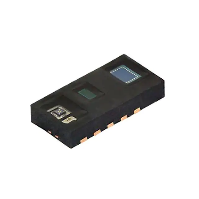
VCNL4020C
www.vishay.com
Vishay Semiconductors
High Resolution Digital Biosensor for Wearable Applications
With I2C Interface
FEATURES
• Package type: surface-mount
• Package form: SMD
• Dimensions (L x W x H in mm): 4.90 x 2.40 x 0.83
• Integrated modules: infrared emitter (IRED),
ambient light sensor (ALS), photo diode (PD),
and signal conditioning IC
• Interrupt function
• Supply voltage range VDD: 2.5 V to 3.6 V
• Supply voltage range IR anode: 2.5 V to 5 V
• Communication via I2C interface
IR anode
1
10 IR cathode
• I2C bus H-level range: 1.7 V to 5 V
SDA
2
9
GND
INT
3
• Floor life: 72 h, MSL 4, according to J-STD-020
8
GND
7
nc
6
nc
SCL
4
VDD
5
• Low stand by current consumption: 1.5 μA
• Material categorization: for definitions of compliance
please see www.vishay.com/doc?99912
22620
OPTICAL BIOSENSORS FUNCTION
DESCRIPTION
The VCNL4020C is a fully integrated biosensor and ambient
light sensor. Fully integrated means that the infrared emitter
is included in the package. It has 16 bit resolution. It
includes a signal processing IC and features standard I2C
communication interface. It features an interrupt function.
• Built-in infrared emitter and broader sensitivity
photodiode allows to also work with green and red LEDs
• 16 bit effective resolution ensures excellent cross talk
immunity
• Programmable LED drive current from 10 mA to 200 mA in
10 mA steps
• Excellent ambient light suppression through signal
modulation
APPLICATIONS
• Wearables
• Health monitoring
AMBIENT LIGHT FUNCTION
• Pulse oximetry
• Built-in
ambient
light
photo-pin-diode
close-to-human-eye sensitivity
with
• 16 bit dynamic range from 0.25 lx to 16 klx
• 100 Hz and 120 Hz flicker noise rejection
PRODUCT SUMMARY
PART
NUMBER
OPERATING
VOLTAGE
RANGE
(V)
I2C BUS
VOLTAGE
RANGE
(V)
LED PULSE
CURRENT (1)
(mA)
AMBIENT
LIGHT
RANGE
(lx)
SPECTRAL
BANDWIDTH
RANGE
λ0.5 (nm)
OUTPUT
CODE
ADC RESOLUTION
BIOSENSOR / AMBIENT
LIGHT SENSOR
2.5 to 3.6
1.7 to 5
10 to 200
0.25 to 16 383
550 to 970
16 bit, I2C
16 bit / 16 bit
VCNL4020C
Note
(1) Adjustable through I2C interface
Rev. 1.1, 20-Mar-18
Document Number: 84350
1
For technical questions, contact: sensorstechsupport@vishay.com
THIS DOCUMENT IS SUBJECT TO CHANGE WITHOUT NOTICE. THE PRODUCTS DESCRIBED HEREIN AND THIS DOCUMENT
ARE SUBJECT TO SPECIFIC DISCLAIMERS, SET FORTH AT www.vishay.com/doc?91000
�VCNL4020C
www.vishay.com
Vishay Semiconductors
ORDERING INFORMATION
ORDERING CODE
VOLUME (1)
PACKAGING
VCNL4020C-GS08
Tape and reel
VCNL4020C-GS18
REMARKS
MOQ: 3300 pcs
4.90 mm x 2.40 mm x 0.83 mm
MOQ: 13 000 pcs
Note
(1) MOQ: minimum order quantity
ABSOLUTE MAXIMUM RATINGS (Tamb = 25 °C, unless otherwise specified)
PARAMETER
SYMBOL
MIN.
MAX.
Supply voltage
TEST CONDITION
VDD
-0.3
5.5
V
Operation temperature range
Tamb
-25
+85
°C
Tstg
-25
+85
°C
Ptot
-
50
mW
Tj
-
100
°C
Storage temperature range
Total power dissipation
Tamb ≤ 25 °C
Junction temperature
UNIT
BASIC CHARACTERISTICS (Tamb = 25 °C, unless otherwise specified)
PARAMETER
MIN.
TYP.
MAX.
UNIT
Supply voltage VDD
TEST CONDITION
SYMBOL
2.5
-
3.6
V
Supply voltage IR anode
2.5
-
5
V
I2C bus H-level range
1.7
-
5
V
INT H-level range
1.7
-
5
V
INT low voltage
3 mA sink current
-
-
0.4
V
Current consumption
Standby current,
no LED-operation
-
1.5
2
μA
2 measurements per second,
LED current 20 mA
-
5
-
μA
250 measurements per second,
LED current 20 mA
-
520
-
μA
2 measurements per second,
LED current 200 mA
-
35
-
μA
250 measurements per second,
LED current 200 mA
-
4
-
mA
2 measurements per second
averaging = 1
-
2.5
-
μA
8 measurements per second
averaging = 1
-
10
-
μA
2 measurements per second
averaging = 64
-
160
-
μA
8 measurements per second
averaging = 64
-
640
-
μA
Digital resolution (LSB count )
-
0.25
-
lx
EV = 100 lx
averaging = 64
-
400
-
counts
-
-
3400
kHz
Current consumption
pulse mode incl. LED
(averaged)
Current consumption ambient
light mode
Ambient light resolution
Ambient light output
I2C clock rate range
Rev. 1.1, 20-Mar-18
fSCL
Document Number: 84350
2
For technical questions, contact: sensorstechsupport@vishay.com
THIS DOCUMENT IS SUBJECT TO CHANGE WITHOUT NOTICE. THE PRODUCTS DESCRIBED HEREIN AND THIS DOCUMENT
ARE SUBJECT TO SPECIFIC DISCLAIMERS, SET FORTH AT www.vishay.com/doc?91000
�VCNL4020C
www.vishay.com
Vishay Semiconductors
CIRCUIT BLOCK DIAGRAM
1
SDA
2
INT
3
SCL
4
VDD
5
30 mm x 30 mm
10 IR cathode
IRED
PD
9
GND
8
GND
7
nc
6
nc
Kodak gray card
(18 % reflectivity)
d = 20 mm
IR anode
TEST CIRCUIT
Ambi
VCNL4020C
ASIC
PD
VCNL4020C
IRED
PD
Note
• nc must not be electrically connected
Pads 6 and 7 are only considered as solder pads
BASIC CHARACTERISTICS (Tamb = 25 °C, unless otherwise specified)
100 000
LED current 200 mA
2.2
10 000
2.0
VDD = 3.6 V
VDD = 3.5 V
VDD = 3.3 V
VDD = 3.1 V
1.8
Proximity Value (cts)
IDD - Supply Current Idle Mode (μA)
2.4
VDD = 2.5 V
VDD = 2.7 V
VDD = 2.9 V
1.6
1.4
LED current 100 mA
100
LED current 20 mA
10
1.2
Media: Kodak gray card
Mod. frequency = 390 kHz
1.0
- 50 - 30 - 10
1
10
30
50
70
90
110
0.1
10
1
100
Tamb - Ambient Temperature (°C)
Distance to Reflecting Card (mm)
Fig. 1 - Idle Current vs. Ambient Temperature
Fig. 3 - Proximity Value vs. Distance
22301
250
IIRED - Forward Current IRED (mA)
2.4
IDD - Supply Current Idle Mode (μA)
1000
100 °C
2.2
2.0
80 °C
1.8
55 °C
1.6
25 °C
1.4
-10 °C
1.2
-40 °C
VIRED = 2.5 V
200 mA
200
160 mA
150
2.4
2.6
2.8
3.0
3.2
3.4
VDD - Supply Voltage (V)
Fig. 2 - Idle Current vs. VDD
Rev. 1.1, 20-Mar-18
3.6
140 mA
120 mA
100 mA
100
80 mA
60 mA
50
1.0
22302
180 mA
40 mA
20 mA
0
-60
3.8
22304
-20
20
60
100
140
Tamb - Ambient Temperature (°C)
Fig. 4 - Forward Current vs. Temperature
Document Number: 84350
3
For technical questions, contact: sensorstechsupport@vishay.com
THIS DOCUMENT IS SUBJECT TO CHANGE WITHOUT NOTICE. THE PRODUCTS DESCRIBED HEREIN AND THIS DOCUMENT
ARE SUBJECT TO SPECIFIC DISCLAIMERS, SET FORTH AT www.vishay.com/doc?91000
�VCNL4020C
www.vishay.com
Vishay Semiconductors
0°
Srel - Relative Sensitivity
0.9
0.8
0.7
0.6
0.5
0.4
0.3
0.2
1.0
0.9
40°
0.8
0.7
60°
0.6
ϕ - Angular Displacement
1.0
80°
0.1
0
750
800
850
900
950
1000
0.5 0.4 0.3 0.2 0.1 0
1050
λ - Wavelength (nm)
22305
22308
Fig. 8 - Relative Radiant Sensitivity vs. Angular Displacement
(Proximity Sensor)
Fig. 5 - Relative Radiant Intensity vs. Wavelength
20°
100 000
1.0
0.9
40°
0.8
0.7
60°
0.6
ϕ - Angular Displacement
0°
Irel - Relative Radiant Intensity
20°
IF = 100 mA
Ambient Light Signal (cts)
Ie, rel - Relative Radiant Intensity
1.1
10 000
1000
100
10
80°
1
0.1
0.5 0.4 0.3 0.2 0.1 0
1
Fig. 6 - Relative Radiant Intensity vs. Angular Displacement
100
1000
10 000
Fig. 9 - Ambient Light Value vs. Illuminance
1.1
S(λ)rel - Relative Spectral Sensitivity
S(λ)rel - Relative Spectral Sensitivity
10
EV - Illuminance (lx)
22306
1.0
0.9
0.8
0.7
0.6
0.5
0.4
0.3
0.2
0.1
0
400
500
600
700
800
900 1000 1100
λ - Wavelength (nm)
Fig. 7 - Relative Spectral Sensitivity vs. Wavelength
(Biosensor)
Rev. 1.1, 20-Mar-18
1.0
Human eye
VCNL4020C
0.8
0.6
0.4
0.2
0
400
500
600
700
800
900
1000 1100
λ - Wavelength (nm)
Fig. 10 - Relative Spectral Sensitivity vs. Wavelength
(Ambient Light Sensor)
Document Number: 84350
4
For technical questions, contact: sensorstechsupport@vishay.com
THIS DOCUMENT IS SUBJECT TO CHANGE WITHOUT NOTICE. THE PRODUCTS DESCRIBED HEREIN AND THIS DOCUMENT
ARE SUBJECT TO SPECIFIC DISCLAIMERS, SET FORTH AT www.vishay.com/doc?91000
�VCNL4020C
www.vishay.com
Vishay Semiconductors
20°
1.0
0.9
40°
Vertical
Horizontal
0.8
0.7
60°
0.6
ϕ - Angular Displacement
Srel - Relative Sensitivity
0°
80°
0.5 0.4 0.3 0.2 0.1 0
22311
Fig. 11 - Relative Radiant Sensitivity vs. Angular Displacement
(Ambient Light Sensor)
APPLICATION INFORMATION
The digital biosensor VCNL4020C needs just one decoupling-C at VDD if connected to a regulated power supply.
IR cathode needs no external connection as the connection to the driver is done internally, but this allows also for adding
external LEDs / IREDs to the driver.
1. Application Circuit
VSMD66694
(2)
IR
(3)
C1
2.5 V
to
3.6 V
(4)
RED
2.5 V
to
5.0 V
(1)
2.5 V
to
3.6 V
C2
R2 R3 R4
22 μF 100 nF
IR anode (1) IR cathode (10)
R1
10R
1.7 V
to
5.0 V
C4
C3
IR anode (1)
VDD (5)
C1
10 μF 100 nF
VCNL4020C
INT (3)
GND (8, 9)
SCL (4)
SDA (2)
Host
Micro Controller
VDD (5)
470 nF
VCNL4020C
GPIO
I2C bus clock SCL
I2C bus data SDA
INT (3)
GND (8, 9)
SCL (4)
SDA (2)
Fig. 12 - Application Circuit
(x) = Pin Number
Note
• The interrupt pin is an open drain output. The needed pull-up resistor may be connected to the same supply voltage as the application
controller and the pull-up resistors at SDA / SCL. Proposed value R2 should be >1 kΩ , e.g. 10 kΩ to 100 kΩ.
Proposed value for R3 and R4, e.g. 2.2 kΩ to 4.7 kΩ, depend also on the I2C bus speed.
For detailed description about set-up and use of the interrupt as well as more application related information see AN: “Designing
VCNL4020C into an Application”.
Rev. 1.1, 20-Mar-18
Document Number: 84350
5
For technical questions, contact: sensorstechsupport@vishay.com
THIS DOCUMENT IS SUBJECT TO CHANGE WITHOUT NOTICE. THE PRODUCTS DESCRIBED HEREIN AND THIS DOCUMENT
ARE SUBJECT TO SPECIFIC DISCLAIMERS, SET FORTH AT www.vishay.com/doc?91000
�VCNL4020C
www.vishay.com
Vishay Semiconductors
2. I2C Interface
The VCNL4020C contains seventeen 8 bit registers for operation control, parameter setup and result buffering. All registers are
accessible via I2C communication. Figure 13 shows the basic I2C communication with VCNL4020C.
The built in I2C interface is compatible with all I2C modes (standard, fast and high speed).
I2C H-level range = 1.7 V to 5 V.
Please refer to the I2C specification from NXP for details.
Send byte
S
Write command to VCNL4020C
Slave address
Receive byte
Wr
A
Register address
Data byte
A
A
P
Read data from VCNL4020C
S
Slave address
Wr
A
Register address
A
P
S
Slave address
Rd
A
Data byte
A
P
S = start condition
P = stop condition
A = acknowledge
Host action
VCNL4020C response
Fig. 13 - Send Byte/Receive Byte Protocol
Device Address
Register Addresses
The VCNL4020C has a fix slave address for the host
programming and accessing selection. The predefined 7 bit
I2C bus address is set to 0010 011 = 13h. The least
significant bit (LSB) defines read or write mode. Accordingly
the bus address is set to 0010 011x = 26h for write, 27h for
read.
VCNL4020C has seventeen user accessible 8 bit registers.
The register addresses are 80h (register #0) to 90h
(register #16).
REGISTER FUNCTIONS
Register #0 Command Register
Register address = 80h
The register #0 is for starting ambient light or biosensor measurements. This register contains 2 flag bits for data ready
indication.
TABLE 1 - COMMAND REGISTER #0
Bit 7
Bit 6
Bit 5
Bit 4
Bit 3
Bit 2
Bit 1
Bit 0
config_lock
als_data_rdy
bs_data_rdy
als_od
bs_od
als_en
bs_en
selftimed_en
Description
config_lock
Read only bit. Value = 1
als_data_rdy
Read only bit. Value = 1 when ambient light measurement data is available in the result registers. This bit
will be reset when one of the corresponding result registers (reg #5, reg #6) is read.
bs_data_rdy
Read only bit. Value = 1 when biosensor measurement data is available in the result registers. This bit
will be reset when one of the corresponding result registers (reg #7, reg #8) is read.
als_od
R/W bit. Starts a single on-demand measurement for ambient light. If averaging is enabled, starts a
sequence of readings and stores the averaged result. Result is available at the end of conversion for
reading in the registers #5(HB) and #6(LB).
bs_od
R/W bit. Starts a single on-demand measurement for biosensor.
Result is available at the end of conversion for reading in the registers #7(HB) and #8(LB).
als_en
R/W bit. Enables periodic als measurement
bs_en
R/W bit. Enables periodic biosensor measurement
selftimed_en
R/W bit. Enables state machine and LP oscillator for self timed measurements; no measurement is
performed until the corresponding bit is set
Note
• With setting bit 3 and bit 4 at the same write command, a simultaneously measurement of ambient light and biosensor is done. Beside als_en
and / or bs_en first selftimed_en needs to be set. On-demand measurement modes are disabled if selftimed_en bit is set. For the
selftimed_en mode changes in reading rates (reg #4 and reg #2) can be made only when b0 (selftimed_en bit) = 0. For the als_od mode
changes to the reg #4 can be made only when b4 (als_od bit) = 0; this is to avoid synchronization problems and undefined states between
the clock domains. In effect this means that it is only reasonable to change rates while no selftimed conversion is ongoing.
Rev. 1.1, 20-Mar-18
Document Number: 84350
6
For technical questions, contact: sensorstechsupport@vishay.com
THIS DOCUMENT IS SUBJECT TO CHANGE WITHOUT NOTICE. THE PRODUCTS DESCRIBED HEREIN AND THIS DOCUMENT
ARE SUBJECT TO SPECIFIC DISCLAIMERS, SET FORTH AT www.vishay.com/doc?91000
�VCNL4020C
www.vishay.com
Vishay Semiconductors
Register #1 Product ID Revision Register
Register address = 81h. This register contains information about product ID and product revision.
Register data value of current revision = 21h.
TABLE 2 - PRODUCT ID REVISION REGISTER #1
Bit 7
Bit 6
Bit 5
Bit 4
Bit 3
Bit 2
Product ID
Bit 1
Bit 0
Bit 1
Bit 0
Revision ID
Description
Product ID
Read only bits. Value = 2
Revision ID
Read only bits. Value = 1
Register #2 Rate of Biosensor Measurement
Register address = 82h.
TABLE 3 - BIOSENSOR RATE REGISTER #2
Bit 7
Bit 6
Bit 5
Bit 4
Bit 3
Bit 2
Rate of biosensor Measurement (no. of
measurements per second)
n/a
Description
Biosensor rate
R/W bits.
000 - 1.95 measurements/s (DEFAULT)
001 - 3.90625 measurements/s
010 - 7.8125 measurements/s
011 - 16.625 measurements/s
100 - 31.25 measurements/s
101 - 62.5 measurements/s
110 - 125 measurements/s
111 - 250 measurements/s
Note
• If self_timed measurement is running, any new value written in this register will not be taken over until the mode is actualy cycled.
Register #3 LED Current Setting for Biosensor Mode
Register address = 83h. This register is to set the LED current value for biosensor measurement.
The value is adjustable in steps of 10 mA from 0 mA to 200 mA.
This register also contains information about the used device fuse program ID.
TABLE 4 - LED CURRENT REGISTER #3
Bit 7
Bit 6
Bit 5
Bit 4
Bit 3
Bit 2
Bit 1
Fuse prog ID
LED current value
Fuse prog ID
Read only bits.
Information about fuse program revision used for initial setup/calibration of the device.
Bit 0
Description
LED current value
Rev. 1.1, 20-Mar-18
R/W bits. LED current = Value (dec.) x 10 mA.
Valid Range = 0 to 20d. e.g. 0 = 0 mA, 1 = 10 mA, …., 20 = 200 mA (2 = 20 mA = DEFAULT)
LED Current is limited to 200 mA for values higher as 20d.
Document Number: 84350
7
For technical questions, contact: sensorstechsupport@vishay.com
THIS DOCUMENT IS SUBJECT TO CHANGE WITHOUT NOTICE. THE PRODUCTS DESCRIBED HEREIN AND THIS DOCUMENT
ARE SUBJECT TO SPECIFIC DISCLAIMERS, SET FORTH AT www.vishay.com/doc?91000
�VCNL4020C
www.vishay.com
Vishay Semiconductors
Register #4 Ambient Light Parameter Register
Register address = 84h.
TABLE 5 - AMBIENT LIGHT PARAMETER REGISTER #4
Bit 7
Bit 6
Cont. conv.
mode
Bit 5
Bit 4
Bit 3
Auto offset
compensation
als_rate
Bit 2
Bit 1
Bit 0
Averaging function
(number of measurements per run)
Description
Cont. conversion mode
Ambient light measurement rate
Auto offset compensation
Averaging function
R/W bit. Continuous conversion mode.
Enable = 1; Disable = 0 = DEFAULT
This function can be used for performing faster ambient light measurements. This mode should only be
used with ambient light on-demand measurements. Do not use with self-timed mode. Please refer to the
application information chapter 3.3 for details about this function.
R/W bits. Ambient light measurement rate
000 - 1 samples/s
001 - 2 samples/s = DEFAULT
010 - 3 samples/s
011 - 4 samples/s
100 - 5 samples/s
101 - 6 samples/s
110 - 8 samples/s
111 - 10 samples/s
R/W bit. Automatic offset compensation.
Enable = 1 = DEFAULT; Disable = 0
In order to compensate a technology, package or temperature related drift of the ambient light values
there is a built in automatic offset compensation function.
With active auto offset compensation the offset value is measured before each ambient light
measurement and subtracted automatically from actual reading.
R/W bits. Averaging function.
Bit values sets the number of single conversions done during one measurement cycle. Result is the
average value of all conversions.
Number of conversions = 2decimal_value e.g. 0 = 1 conv., 1 = 2 conv, 2 = 4 conv., ….7 = 128 conv.
DEFAULT = 32 conv. (bit 2 to bit 0: 101)
Note
• If self_timed measurement is running, any new value written in this register will not be taken over until the mode is actualy cycled.
Register #5 and #6 Ambient Light Result Register
Register address = 85h and 86h. These registers are the result registers for ambient light measurement readings.
The result is a 16 bit value. The high byte is stored in register #5 and the low byte in register #6.
TABLE 6 - AMBIENT LIGHT RESULT REGISTER #5
Bit 7
Bit 6
Bit 5
Bit 4
Bit 3
Bit 2
Bit 1
Bit 0
Bit 1
Bit 0
Description
Read only bits. High byte (15:8) of ambient light measurement result
TABLE 7 - AMBIENT LIGHT RESULT REGISTER #6
Bit 7
Bit 6
Bit 5
Bit 4
Bit 3
Bit 2
Description
Read only bits. Low byte (7:0) of ambient light measurement result
Rev. 1.1, 20-Mar-18
Document Number: 84350
8
For technical questions, contact: sensorstechsupport@vishay.com
THIS DOCUMENT IS SUBJECT TO CHANGE WITHOUT NOTICE. THE PRODUCTS DESCRIBED HEREIN AND THIS DOCUMENT
ARE SUBJECT TO SPECIFIC DISCLAIMERS, SET FORTH AT www.vishay.com/doc?91000
�VCNL4020C
www.vishay.com
Vishay Semiconductors
Register #7 and #8 Biosensor Measurement Result Register
Register address = 87h and 88h. These registers are the result registers for biosensor measurement readings.
The result is a 16 bit value. The high byte is stored in register #7 and the low byte in register #8.
TABLE 8 - BIOSENSOR RESULT REGISTER #7
Bit 7
Bit 6
Bit 5
Bit 4
Bit 3
Bit 2
Bit 1
Bit 0
Bit 1
Bit 0
Description
Read only bits. High byte (15:8) of biosensor measurement result
TABLE 9 - BIOSENSOR RESULT REGISTER #8
Bit 7
Bit 6
Bit 5
Bit 4
Bit 3
Bit 2
Description
Read only bits. Low byte (7:0) of biosensor measurement result
Register #9 Interrupt Control Register
Register address = 89h.
TABLE 10 - INTERRUPT CONTROL REGISTER #9
Bit 7
Bit 6
Int count exceed
Bit 5
Bit 4
Bit 3
Bit 2
Bit 1
Bit 0
n/a
INT_BS_
ready_EN
INT_ALS_
ready_EN
INT_THRES_EN
INT_THRES_
SEL
Description
Int count exceed
INT_BS_ready_EN
INT_ALS_ ready_EN
R/W bits. These bits contain the number of consecutive measurements needed above/below the
threshold
000 - 1 count = DEFAULT
001 - 2 count
010 - 4 count
011 - 8 count
100 -16 count
101 - 32 count
110 - 64 count
111 - 128 count
R/W bit. Enables interrupt generation at biosensor data ready
R/W bit. Enables interrupt generation at ambient data ready
INT_THRES_EN
R/W bit. Enables interrupt generation when high or low threshold is exceeded
INT_THRES_SEL
R/W bit. If 0: thresholds are applied to biosensor measurements
If 1: thresholds are applied to als measurements
Rev. 1.1, 20-Mar-18
Document Number: 84350
9
For technical questions, contact: sensorstechsupport@vishay.com
THIS DOCUMENT IS SUBJECT TO CHANGE WITHOUT NOTICE. THE PRODUCTS DESCRIBED HEREIN AND THIS DOCUMENT
ARE SUBJECT TO SPECIFIC DISCLAIMERS, SET FORTH AT www.vishay.com/doc?91000
�VCNL4020C
www.vishay.com
Vishay Semiconductors
Register #10 and #11 Low Threshold
Register address = 8Ah and 8Bh. These registers contain the low threshold value. The value is a 16 bit word. The high byte is
stored in register #10 and the low byte in register #11.
TABLE 11 - LOW THRESHOLD REGISTER #10
Bit 7
Bit 6
Bit 5
Bit 4
Bit 3
Bit 2
Bit 1
Bit 0
Bit 2
Bit 1
Bit 0
Description
R/W bits. High byte (15:8) of low threshold value
TABLE 12 - LOW THRESHOLD REGISTER #11
Bit 7
Bit 6
Bit 5
Bit 4
Bit 3
Description
R/W bits. Low byte (7:0) of low threshold value
Register #12 and #13 High Threshold
Register address = 8Ch and 8Dh. These registers contain the high threshold value. The value is a 16 bit word. The high byte is
stored in register #12 and the low byte in register #13.
TABLE 13 - HIGH THRESHOLD REGISTER #12
Bit 7
Bit 6
Bit 5
Bit 4
Bit 3
Bit 2
Bit 1
Bit 0
Bit 1
Bit 0
Description
R/W bits. High byte (15:8) of high threshold value
TABLE 14 - HIGH THRESHOLD REGISTER #13
Bit 7
Bit 6
Bit 5
Bit 4
Bit 3
Bit 2
Description
R/W bits. Low byte (7:0) of high threshold value
Register #14 Interrupt Status Register
Register address = 8Eh. This register contains information about the interrupt status for either biosensor or ALS function and
indicates if high or low going threshold exceeded.
TABLE 15 - INTERRUPT STATUS REGISTER #14
Bit 7
Bit 6
Bit 5
n/a
Bit 4
Bit 3
Bit 2
Bit 1
Bit 0
int_bs_ready
int_als_ready
int_th_low
int_th_hi
Description
int_bs_ready
R/W bit. Indicates a generated interrupt for biosensor
int_als_ready
R/W bit. Indicates a generated interrupt for als
int_th_low
R/W bit. Indicates a low threshold exceed
int_th_hi
R/W bit. Indicates a high threshold exceed
Note
• Once an interrupt is generated the corresponding status bit goes to 1 and stays there unless it is cleared by writing a 1 in the corresponding
bit. The int pad will be pulled down while at least one of the status bit is 1.
Rev. 1.1, 20-Mar-18
Document Number: 84350
10
For technical questions, contact: sensorstechsupport@vishay.com
THIS DOCUMENT IS SUBJECT TO CHANGE WITHOUT NOTICE. THE PRODUCTS DESCRIBED HEREIN AND THIS DOCUMENT
ARE SUBJECT TO SPECIFIC DISCLAIMERS, SET FORTH AT www.vishay.com/doc?91000
�VCNL4020C
www.vishay.com
Vishay Semiconductors
Register #15 Biosensor Modulator Timing Adjustment
Register address = 8Fh.
TABLE 16 - BIOSENSOR MODULATOR TIMING ADJUSTMENT #15
Bit 7
Bit 6
Bit 5
Bit 4
Modulation delay time
Bit 3
Bit 2
Biosensor frequency
Bit 1
Bit 0
Modulation dead time
Description
Modulation delay time
R/W bits. Setting a delay time between LED signal and detectors input signal evaluation.
This function is for compensation of delays from LED and photo diode. Also in respect to the possibility
for setting different proximity signal frequency. Correct adjustment is optimizing measurement signal
level. (DEFAULT = 0)
Biosensor frequency
R/W bits. Setting the biosensor test signal frequency
The biosensor measurement is using a square signal as measurement signal. Four different values are
possible:
00 = 390.625 kHz (DEFAULT)
01 = 781.25 kHz
10 = 1.5625 MHz
11 = 3.125 MHz
Modulation dead time
R/W bits. Setting a dead time in evaluation of LED signal at the slopes of the signal. (DEFAULT = 1)
This function is for reducing of possible disturbance effects.
This function is reducing signal level and should be used carefully.
Note
• The settings for best performance will be provided by Vishay. With first samples this is evaluated to:
Delay time = 0; dead time = 1 and BS frequency = 00. With that register #15 should be programmed with 1 (= default value).
Register #16 Ambient IR Light Level Register
Register address = 90h.
This register is not intended to be used by customer.
3. IMPORTANT APPLICATION HINTS AND EXAMPLES
3.1 Receiver standby mode
In standby mode the receiver has the lowest current consumption of about 1.5 μA. In this mode only the I2C interface is active.
This is always valid, when there are no measurement demands executed. Also the current sink for the LED is inactive, so there
is no need for changing register #3 (LED current).
3.2 Data Read
In order to get a certain register value, the register has to be addressed without data like shown in the following scheme. After
this register addressing, the data from the addressed register is written after a subsequent read command.
Receive byte
Read data from VCNL4020C
S
Slave address
Wr
A
Register address
A
P
S
Slave address
Rd
A
Data byte
A
P
S = start condition
P = stop condition
A = acknowledge
Host action
VCNL4020C response
Fig. 14 - Send Byte / Receive Byte Protocol
The stop condition between these write and read sequences is not mandatory. It works also with a repeated start condition.
Note
• For reading out 2 (or more) subsequent registers like the result registers, it is not necessary to address each of the registers separately. After
one read command the internal register counter is increased automatically and any subsequent read command is accessing the next
register.
Rev. 1.1, 20-Mar-18
Document Number: 84350
11
For technical questions, contact: sensorstechsupport@vishay.com
THIS DOCUMENT IS SUBJECT TO CHANGE WITHOUT NOTICE. THE PRODUCTS DESCRIBED HEREIN AND THIS DOCUMENT
ARE SUBJECT TO SPECIFIC DISCLAIMERS, SET FORTH AT www.vishay.com/doc?91000
�VCNL4020C
www.vishay.com
Vishay Semiconductors
Example: read register “Ambient Light Result Register” #5 and #6:
Addressing:command: 26h, 85h (VCNL4020C_I2C_Bus_Write_Adr., Ambient Light Result Register #5 [85])
Read register #5:command: 27h, data (VCNL4020C_I2C_Bus_Read_Adr., {High Byte Data of Ambient Light Result register #5
[85])}
Read register #6:command: 27h, data (VCNL4020C_I2C_Bus_Read_Adr., {Low Byte Data of Ambient Light Result register #6
[86])}
3.3 Continuous Conversion Mode in Ambient Light Measurement
In the following is a detail description of the function “continuous conversion” (bit 7 of register #4)
Standard mode (bit 7 of reg #4 = 0):
In standard mode the ambient light measurement is done during a fixed time frame of 100 ms. The single measurement itself
takes actually only appr. 300 μs.
The following figures show examples of this measurement timing in standard mode using averaging function 2 and 8 as
examples for illustration (possible values up to 128).
Start
Start
50 ms
12.5 ms
100 ms
100 ms
22316
22315
Fig. 15 - Ambient Light Measurement with Averaging = 2;
Final Measurement Result = Average of these 2 Measurements
Fig. 16 - Ambient Light Measurement with Averaging = 8;
Final Measurement Result = Average of these 8 Measurements
Note
• ≥ Independent of setting of averaging the result is available only after 100 ms.
Continuous conversion mode (bit 7 of register #4 = 1):
In continuous conversion mode the single measurements are done directly subsequent after each other.
See following examples in figure 17 and 18
Start
Start
460 μs
460 μs
1.5 ms
4.2 ms
22317
22318
Fig. 17 - Ambient Light Measurement with Averaging = 2;
using Continuous Conversion Mode
Rev. 1.1, 20-Mar-18
Fig. 18 - Ambient Light Measurement with Averaging = 8;
using Continuous Conversion Mode
Document Number: 84350
12
For technical questions, contact: sensorstechsupport@vishay.com
THIS DOCUMENT IS SUBJECT TO CHANGE WITHOUT NOTICE. THE PRODUCTS DESCRIBED HEREIN AND THIS DOCUMENT
ARE SUBJECT TO SPECIFIC DISCLAIMERS, SET FORTH AT www.vishay.com/doc?91000
�VCNL4020C
www.vishay.com
Vishay Semiconductors
PACKAGE DIMENSIONS in millimeters
4.15
VDD
SCL
INT
Cathode
PD
Cathode
PD
VDD
SCL
VSS
INT
SDA
Anode
Emitter
0.83
0.15
technical drawings
according to DIN
specifications
Proposed PCB Footprint
(4.9)
0.69
1.75
0.83
Not indicated tolerances ± 0.1
0.2
0.2
0.45
0.4
0.8
Drawing-No.: 6.550-5319
(2.4)
1.27
4.9
1.1
0.4
0.28
1.5
2.4
0.37
0.4
0.25
0.8
2.03
Rev. 1.1, 20-Mar-18
VSS
Anode
Emitter
Cathode
Emitter
Pinning Top view
Cathode
Emitter
0.78
0.73 0.95 0.98
1.49 1.62
0.24
0.3
0.65
0.55
0.685
SDA
Pinning Bottom view
4x0.685=2.74
4x 0.685=2.74
Document Number: 84350
13
For technical questions, contact: sensorstechsupport@vishay.com
THIS DOCUMENT IS SUBJECT TO CHANGE WITHOUT NOTICE. THE PRODUCTS DESCRIBED HEREIN AND THIS DOCUMENT
ARE SUBJECT TO SPECIFIC DISCLAIMERS, SET FORTH AT www.vishay.com/doc?91000
�VCNL4020C
www.vishay.com
Vishay Semiconductors
TAPE AND REEL DIMENSIONS in millimeters
Rev. 1.1, 20-Mar-18
Document Number: 84350
14
For technical questions, contact: sensorstechsupport@vishay.com
THIS DOCUMENT IS SUBJECT TO CHANGE WITHOUT NOTICE. THE PRODUCTS DESCRIBED HEREIN AND THIS DOCUMENT
ARE SUBJECT TO SPECIFIC DISCLAIMERS, SET FORTH AT www.vishay.com/doc?91000
�VCNL4020C
www.vishay.com
Vishay Semiconductors
SOLDER PROFILE
DRYPACK
Devices are packed in moisture barrier bags (MBB) to
prevent the products from moisture absorption during
transportation and storage. Each bag contains a desiccant.
Axis Title
10000
300
Max. 260 °C
255 °C
240 °C
217 °C
245 °C
FLOOR LIFE
1000
200
Max. 30 s
1st line
2nd line
2nd line
Temperature (°C)
250
150
Max. 120 s
100
Max. 100 s
Max. ramp down 6 °C/s
100
Floor life (time between soldering and removing from MBB)
must not exceed the time indicated on MBB label:
Floor life: 72 h
Conditions: Tamb < 30 °C, RH < 60 %
Moisture sensitivity level 4, according to J-STD-020.
Max. ramp up 3 °C/s
50
DRYING
10
0
0
50
100
150
200
250
300
Time (s)
19841
Fig. 19 - Lead (Pb)-free Reflow Solder Profile
According to J-STD-020
Rev. 1.1, 20-Mar-18
In case of moisture absorption devices should be baked
before soldering. Conditions see J-STD-020 or label.
Devices taped on reel dry using recommended conditions
192 h at 40 °C (+ 5 °C), RH < 5 %.
Document Number: 84350
15
For technical questions, contact: sensorstechsupport@vishay.com
THIS DOCUMENT IS SUBJECT TO CHANGE WITHOUT NOTICE. THE PRODUCTS DESCRIBED HEREIN AND THIS DOCUMENT
ARE SUBJECT TO SPECIFIC DISCLAIMERS, SET FORTH AT www.vishay.com/doc?91000
�Legal Disclaimer Notice
www.vishay.com
Vishay
Disclaimer
ALL PRODUCT, PRODUCT SPECIFICATIONS AND DATA ARE SUBJECT TO CHANGE WITHOUT NOTICE TO IMPROVE
RELIABILITY, FUNCTION OR DESIGN OR OTHERWISE.
Vishay Intertechnology, Inc., its affiliates, agents, and employees, and all persons acting on its or their behalf (collectively,
“Vishay”), disclaim any and all liability for any errors, inaccuracies or incompleteness contained in any datasheet or in any other
disclosure relating to any product.
Vishay makes no warranty, representation or guarantee regarding the suitability of the products for any particular purpose or
the continuing production of any product. To the maximum extent permitted by applicable law, Vishay disclaims (i) any and all
liability arising out of the application or use of any product, (ii) any and all liability, including without limitation special,
consequential or incidental damages, and (iii) any and all implied warranties, including warranties of fitness for particular
purpose, non-infringement and merchantability.
Statements regarding the suitability of products for certain types of applications are based on Vishay's knowledge of typical
requirements that are often placed on Vishay products in generic applications. Such statements are not binding statements
about the suitability of products for a particular application. It is the customer's responsibility to validate that a particular product
with the properties described in the product specification is suitable for use in a particular application. Parameters provided in
datasheets and / or specifications may vary in different applications and performance may vary over time. All operating
parameters, including typical parameters, must be validated for each customer application by the customer's technical experts.
Product specifications do not expand or otherwise modify Vishay's terms and conditions of purchase, including but not limited
to the warranty expressed therein.
Hyperlinks included in this datasheet may direct users to third-party websites. These links are provided as a convenience and
for informational purposes only. Inclusion of these hyperlinks does not constitute an endorsement or an approval by Vishay of
any of the products, services or opinions of the corporation, organization or individual associated with the third-party website.
Vishay disclaims any and all liability and bears no responsibility for the accuracy, legality or content of the third-party website
or for that of subsequent links.
Except as expressly indicated in writing, Vishay products are not designed for use in medical, life-saving, or life-sustaining
applications or for any other application in which the failure of the Vishay product could result in personal injury or death.
Customers using or selling Vishay products not expressly indicated for use in such applications do so at their own risk. Please
contact authorized Vishay personnel to obtain written terms and conditions regarding products designed for such applications.
No license, express or implied, by estoppel or otherwise, to any intellectual property rights is granted by this document or by
any conduct of Vishay. Product names and markings noted herein may be trademarks of their respective owners.
© 2022 VISHAY INTERTECHNOLOGY, INC. ALL RIGHTS RESERVED
Revision: 01-Jan-2022
1
Document Number: 91000
�


 工商网监
湘ICP备2023018690号
工商网监
湘ICP备2023018690号
