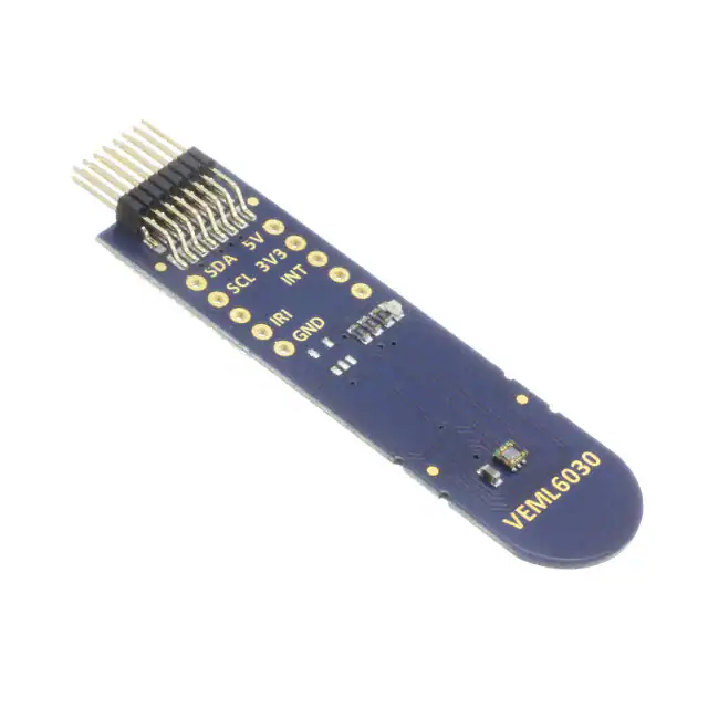
VEML6030
www.vishay.com
Vishay Semiconductors
High Accuracy Ambient Light Sensor With I2C Interface
FEATURES
• Package type: surface-mount
• Dimensions (L x W x H in mm): 2 x 2 x 0.87
• Integrated modules: ambient light sensor (ALS)
• Supply voltage range VDD: 2.5 V to 3.6 V
• Communication via I2C interface
• I2C bus H-level range: 1.7 V to 3.6 V
• Floor life: 72 h, MSL 4, according to J-STD-020
• Low stand by current consumption: typ. 0.5 μA
• Material categorization: for definitions of
compliance please see www.vishay.com/doc?99912
DESCRIPTION
AMBIENT LIGHT FUNCTION
VEML6030 is a high accuracy ambient light digital 16-bit
resolution sensor in a miniature transparent 2 mm x 2 mm
package. It includes a high sensitive photodiode, a low
noise amplifier, a 16-bit A/D converter and supports an
easy to use I2C bus communication interface and additional
interrupt feature.
• FiltronTM technology adaption: close to real human eye
response
• O-TrimTM technology adoption: ALS output tolerance
≤ 10 %
The ambient light result is as digital value available.
• 16-bit dynamic range for ambient light detection from
0 lx to about 120 klx with resolution down to 0.0036 lx/ct,
supports low transmittance (dark) lens design
APPLICATIONS
• 100 Hz and 120 Hz flicker noise rejection
• Ambient light sensor for mobile devices (e.g. smart
phones, touch phones, PDA, GPS) for backlight dimming
• Excellent temperature compensation
• Ambient light sensor for industrial on- / off-lighting
operation
• Software shutdown mode control
• High dynamic detection resolution
• Optical switch for consumer, computing, and industrial
devices and displays
PRODUCT SUMMARY
PART NUMBER
VEML6030
OPERATING
RANGE
(mm)
OPERATING
VOLTAGE
RANGE
(V)
I2C BUS
VOLTAGE
RANGE
(V)
AMBIENT
LIGHT RANGE
(lx)
AMBIENT
LIGHT
RESOLUTION
(lx)
OUTPUT
CODE
ADC RESOLUTION
PROXIMITY /
AMBIENT LIGHT
n/a
2.5 to 3.6
1.7 to 3.6
0 to 120 000
0.0036
16 bit, I2C
- / 0.0036
ORDERING INFORMATION
ORDERING CODE
VEML6030
VEML6030-GS15
PACKAGING
Tape and reel
VOLUME (1)
MOQ: 3000
MOQ: 10 000
REMARKS
2.0 mm x 2.0 mm x 0.87 mm
Note
(1) MOQ: minimum order quantity
Rev. 1.6, 28-Apr-2022
Document Number: 84366
1
For technical questions, contact: sensorstechsupport@vishay.com
THIS DOCUMENT IS SUBJECT TO CHANGE WITHOUT NOTICE. THE PRODUCTS DESCRIBED HEREIN AND THIS DOCUMENT
ARE SUBJECT TO SPECIFIC DISCLAIMERS, SET FORTH AT www.vishay.com/doc?91000
�VEML6030
www.vishay.com
Vishay Semiconductors
ABSOLUTE MAXIMUM RATINGS (Tamb = 25 °C, unless otherwise specified)
PARAMETER
SYMBOL
MIN.
MAX.
UNIT
Supply voltage
TEST CONDITION
VDD
0
4
V
Operation temperature range
Tamb
-25
+85
°C
Storage temperature range
Tstg
-25
+85
°C
Ptot
-
50
mW
Tj
-
110
°C
Tamb ≤ 25 °C
Total power dissipation
Junction temperature
BASIC CHARACTERISTICS (Tamb = 25 °C, unless otherwise specified)
PARAMETER
TEST CONDITION
SYMBOL
MIN.
TYP.
MAX.
VDD
2.5
3.3
3.6
V
VDD is 3.3 V
Isd
-
0.5
-
μA
VDD is 3.3 V, PSM = 11, refresh time 4100 ms
IDD
-
2
-
μA
VDD is 3.3 V, PSM = 00, refresh time 600 ms
IDD
-
8
-
μA
VDD is 3.3 V, PSM_EN = 0, refresh time 100 ms
IDD
-
45
-
μA
kHz
Supply voltage
Shut down current (2)
Operation mode current
(1)
I2C clock rate range
UNIT
fSCL
10
-
400
I2C bus input H-level range
VDD is 3.3 V
Vih
1.3
-
3.6
V
I2C bus input L-level range
VDD is 3.3 V
Vil
-0.3
-
0.4
V
Iol
3
-
-
mA
lx/step
Digital current out
(low, current sink)
Digital resolution (LSB count)
with ALS_GAIN = “01”
-
0.0036
-
Detectable minimum illuminance
with ALS_GAIN = “01”
EV min.
-
0.0072
-
lx
Detectable maximum illuminance
with ALS_GAIN = “10”
EV max.
-
120 000
-
lx
Dark offset (2)
with ALS_GAIN = “01”
-
3
-
step
Notes
(1) Light source: white LED
(2) Light conditions: dark
CIRCUIT BLOCK DIAGRAM
VEML6030
GND 1
6 VDD
Temperature
sensor
Low pass
filter
SDA 2
Timing
controller
Output buffer
I2C interface
ALS-PD
INT 3
5 SCL
4 ADDR
Oscillator
Fig. 1 - Block Diagram
Rev. 1.6, 28-Apr-2022
Document Number: 84366
2
For technical questions, contact: sensorstechsupport@vishay.com
THIS DOCUMENT IS SUBJECT TO CHANGE WITHOUT NOTICE. THE PRODUCTS DESCRIBED HEREIN AND THIS DOCUMENT
ARE SUBJECT TO SPECIFIC DISCLAIMERS, SET FORTH AT www.vishay.com/doc?91000
�VEML6030
www.vishay.com
Vishay Semiconductors
I2C TIMING CHARACTERISTICS (Tamb = 25 °C, unless otherwise specified)
PARAMETER
SYMBOL
Clock frequency
STANDARD MODE (1)
MIN.
MAX.
f(SMBCLK)
10
t(BUF)
4.7
t(HDSTA)
Repeated start condition setup time
Stop condition setup time
Data hold time
Data setup time
I2C clock (SCK) low period
I2C clock (SCK) high period
UNIT
MAX.
100
10
400
kHz
-
1.3
-
μs
4.0
-
0.6
-
μs
t(SUSTA)
4.7
-
0.6
-
μs
t(SUSTO)
4.0
-
0.6
-
μs
t(HDDAT)
0
3450
0
900
ns
t(SUDAT)
250
-
100
-
ns
t(LOW)
4.7
-
1.3
-
μs
Bus free time between start and stop condition
Hold time after (repeated) start condition;
after this period, the first clock is generated
FAST MODE (1)
MIN.
t(HIGH)
4.0
-
0.6
-
μs
t(TIMEOUT)
25
35
-
-
ms
Clock / data fall time
t(F)
-
300
-
300
ns
Clock / data rise time
t(R)
-
1000
-
300
ns
Detect clock / data low timeout
Note
(1) Data based on standard I2C protocol requirement, not tested in production
t(LOW)
I2C bus
clock
(SLCK)
t(R)
t(F)
VIH
VIL
t(HDSTA)
t(HIGH)
t(SUSTA)
t(SUSTO)
t(BUF)
t(HDDAT)
I2C bus
data
(SDAT)
t(SUDAT)
VIH
Start
{
S
Start condition
{
P
Stop condition
{
{
VIL
S
P
Stop
t(LOSEXT)
SCLKACK
t(LOWMEXT)
SDAACK
t(LOWMEXT)
t(LOWMEXT)
I2C bus
clock
(SLCK)
I2C bus
data
(SDAT)
Fig. 2 - I2C Timing Diagram
Rev. 1.6, 28-Apr-2022
Document Number: 84366
3
For technical questions, contact: sensorstechsupport@vishay.com
THIS DOCUMENT IS SUBJECT TO CHANGE WITHOUT NOTICE. THE PRODUCTS DESCRIBED HEREIN AND THIS DOCUMENT
ARE SUBJECT TO SPECIFIC DISCLAIMERS, SET FORTH AT www.vishay.com/doc?91000
�VEML6030
www.vishay.com
Vishay Semiconductors
PARAMETER TIMING INFORMATION
I2C bus
clock
(SCLK)
I2C bus
data
(SDAT)
SA7
SA6
SA5
SA4
SA3
SA2
SA1
SA7
W
SA6
SA5
SA4
SA3
SA2
SA1
SA0
ACK
Start by
master
ACK
I2C bus slave address byte
Command code
I2C bus
clock
(SCLK)
I2C bus
data
(SDAT)
SA7
SA6
SA5
SA4
SA3
SA2
SA1
SA0
SA6
SA7
SA5
SA4
SA3
SA2
SA1
SA0
ACK
ACK
Data byte low
Stop by
master
Data byte high
Fig. 3 - I2C Bus Timing for Sending Word Command Format
I2C bus
clock
(SCLK)
I2C bus
data
(SDAT)
SA7
SA6
SA5
SA4
SA3
SA2
SA1
SA7
W
SA6
SA5
SA4
SA3
SA2
SA1
SA0
ACK
Start by
master
ACK
I2C bus slave address byte
Command code
I2C bus
clock
(SCLK)
I2C bus
data
(SDAT)
SA7
SA6
SA5
SA4
SA3
SA2
R
SA1
SA7
SA6
SA5
SA4
SA3
ACK
Start by
master
SA2
SA1
SA0
ACK by
master
I2C bus slave address byte
Data byte low
I2C bus
clock
(SCLK)
I2C bus
data
(SDAT)
SA7
SA6
SA5
SA4
SA3
SA2
SA1
SA0
NACK by
master
Stop by
master
Data byte high
Fig. 4 - I2C Bus Timing for Receive Word Command Format
Rev. 1.6, 28-Apr-2022
Document Number: 84366
4
For technical questions, contact: sensorstechsupport@vishay.com
THIS DOCUMENT IS SUBJECT TO CHANGE WITHOUT NOTICE. THE PRODUCTS DESCRIBED HEREIN AND THIS DOCUMENT
ARE SUBJECT TO SPECIFIC DISCLAIMERS, SET FORTH AT www.vishay.com/doc?91000
�VEML6030
www.vishay.com
Vishay Semiconductors
BASIC CHARACTERISTICS (Tamb = 25 °C, unless otherwise specified)
Axis Title
120
VEML6030
80
60
V(λ)
40
20
0
400
500
600
700
800
900
1000
90
80
70
1000
60
1st line
2nd line
2nd line
S(λ)φ, rel - Relative Spectral Sensitivity
100
Normalized Responsivity
10000
100
50
40
100
30
20
10
10
0
λ - Wavelength (nm)
350
450
550
650
750
850
950 1050
λ - Wavelength (nm)
Fig. 5 - Spectral Response
Fig. 6 - White Channel Responsivity
ALS sensitivity spectrum close to human eye photopic curve V(λ). Human eye curve adaption achieved by Filtron technology.
0°
20°
0.9
40°
0.8
0.7
60°
0.6
80°
nom. -10 %
nom.
nom. +10 %
100
Reading of ALS (klx)
1.0
ϕ - Angular Displacement
Srel - Relative Sensitivity
120
80
60
40
20
0
0
0.5 0.4 0.3 0.2 0.1 0
20
40
60
80
100
120
Brightness Acc. Calibrated Luxmeter (klx)
22308
Fig. 7 - Relative Radiant Sensitivity vs. Angular Displacement
Rev. 1.6, 28-Apr-2022
Fig. 8 - ALS measurement deviation between different light sources:
≤ 10 %
Document Number: 84366
5
For technical questions, contact: sensorstechsupport@vishay.com
THIS DOCUMENT IS SUBJECT TO CHANGE WITHOUT NOTICE. THE PRODUCTS DESCRIBED HEREIN AND THIS DOCUMENT
ARE SUBJECT TO SPECIFIC DISCLAIMERS, SET FORTH AT www.vishay.com/doc?91000
�VEML6030
www.vishay.com
Vishay Semiconductors
APPLICATION INFORMATION
VEML6030 is a cost effective solution of ambient light sensor with I2C bus interface. The standard serial digital interface is easy
to access “Ambient Light Signal” without complex calculation and programming by external controller. Beside the digital output
also a flexible programmable interrupt pin is available.
1. Application Circuit
1.7 V to 3.6 V
R1 R2 R3
GND (1)
2.5 V to 3.6 V
R4
C1
10R
C2
VDD (6)
10 μF 100 nF
C1 and R4
are optional
for very
disturbed
supply
Host
Micro Controller
VEML6030
SDA (2)
I2C bus data SDA
SCL (5)
I2C bus clock SCL
ADDR (4)
INT (3)
GPIO (interrupt)
Fig. 9 - Application Circuit
(x) = Pin Number
Notes
• The interrupt pin is an open drain output. Proposed values for the pull-up resistors should be > 1 kΩ, e.g. 2.2 kΩ to 4.7 kΩ for the R1 and
R2 (at SDA and SCL) and 10 kΩ to 100 kΩ for R3 (at interrupt).
Normally just one decoupling capacitor is needed. This should be ≥ 100 nF and placed close to the VDD pin.
Pin ADDR allows for the device addresses: pin 4 = high (VDD) = 0x48, pin 4 = low (GND) = 0x10
For detailed description about set-up and use of the interrupt as well as more application related information see AN: “Designing VEML6030
into an Application”
2. I2C Interface
The VEML6030 contains actual six 16 bit command codes for operation control, parameter setup, and result buffering. All
registers are accessible via I2C communication. Figure 7 shows the basic I2C communication with VEML6030.
The built in I2C interface is compatible with I2C modes “standard” and “fast”: 10 kHz to 400 kHz.
I2C H-level range = 1.3 V to 3.6 V.
Please refer to the I2C specification from NXP for details.
Send byte
S
Slave address
Receive byte
S
Write command to VEML6030
Wr
A
Command code
A
Data byte (LSB)
A
Data byte (MSB)
A
P
Read data from VEML6030
Slave address
S = start condition
P = stop condition
A = acknowledge
N = no acknowledge
Wr
A
A
Command code
S
Slave address
Rd
A
Data byte (LSB)
A
Data byte (MSB)
N
P
Host action
VEML6030 response
Fig. 10 - Send Byte / Receive Byte Protocol
Device Address
The VEML6030 has two fix slave addresses for the host
programming and accessing selection.
With ADDR pin plugged to power supply = high = VDD, the
predefined 7 bit I2C bus address is set to 1001000 = 0x48.
The least significant bit (LSB) defines read or write mode.
Rev. 1.6, 28-Apr-2022
Accordingly the bus address is set to 1001 0000 = 90h for
write and 1001 0001 = 91h for read.
With ADDR pin plugged to ground = low, the slave address
(7 bit) is set to 0010000 = 0x10. According 8 bit the bus
address is then 0010 0000 = 20h for write and 0010 0001 =
21h for read.
Document Number: 84366
6
For technical questions, contact: sensorstechsupport@vishay.com
THIS DOCUMENT IS SUBJECT TO CHANGE WITHOUT NOTICE. THE PRODUCTS DESCRIBED HEREIN AND THIS DOCUMENT
ARE SUBJECT TO SPECIFIC DISCLAIMERS, SET FORTH AT www.vishay.com/doc?91000
�VEML6030
www.vishay.com
Vishay Semiconductors
Register Addresses
Auto-Memorization
VEML6030 has actual six user accessible 16 bit command
codes.
VEML6030 can memorize the last ambient data before
shutdown and keep this data before waking up.
The addresses are 00h to 06h (03h not defined / reserved).
When VEML6030 is in shutdown mode, the host can freely
read this data via read command directly.
When VEML6030 wakes up, the data will be refreshed by
new detection.
COMMAND REGISTER FORMAT
COMMAND CODE
REGISTER NAME
BIT
00
ALS_CONF 0
15 : 0
ALS gain, integration time, interrupt, and shut down
W
15 : 8
ALS high threshold window setting (MSB)
W
W
01
ALS_WH
02
ALS_WL
03
Power saving
04
ALS
05
WHITE
06
ALS_INT
FUNCTION / DESCRIPTION
R/W
7:0
ALS high threshold window setting (LSB)
15 : 8
ALS low threshold window setting (MSB)
W
7:0
ALS low threshold window setting (LSB)
W
15 : 0
Set (15 : 3) 0000 0000 0000 0b
15 : 8
MSB 8 bits data of whole ALS 16 bits
R
7:0
LSB 8 bits data of whole ALS 16 bits
R
15 : 8
MSB 8 bits data of whole WHITE 16 bits
R
7:0
LSB 8 bits data of whole WHITE 16 bits
R
15 : 0
ALS INT trigger event
R
Note
• Command code 0 default value is 01 = devices is shut down
Command Code #0: Configuration Register
Register address = 00h
The command code #0 is for configuration of the ambient light measurements.
TABLE 1 - CONFIGURATION REGISTER #0
REGISTER NAME
BIT
Reserved
15 : 13
Set 000b
W
ALS_GAIN
12 : 11
Gain selection
00 = ALS gain x 1
01 = ALS gain x 2
10 = ALS gain x (1/8)
11 = ALS gain x (1/4)
W
reserved
10
Set 0b
W
9:6
ALS integration time setting
1100 = 25 ms
1000 = 50 ms
0000 = 100 ms
0001 = 200 ms
0010 = 400 ms
0011 = 800 ms
W
ALS_PERS
5:4
ALS persistence protect number setting
00 = 1
01 = 2
10 = 4
11 = 8
W
Reserved
3:2
Set 00b
W
W
W
ALS_IT
FUNCTION / DESCRIPTION
ALS_INT_EN
1
ALS interrupt enable setting
0 = ALS INT disable
1 = ALS INT enable
ALS_SD
0
ALS shut down setting
0 = ALS power on
1 = ALS shut down
R/W
Note
• Light level [lx] is (ALS OUTPUT DATA [dec.] / ALS Gain x responsivity). Please study also the application note
Rev. 1.6, 28-Apr-2022
Document Number: 84366
7
For technical questions, contact: sensorstechsupport@vishay.com
THIS DOCUMENT IS SUBJECT TO CHANGE WITHOUT NOTICE. THE PRODUCTS DESCRIBED HEREIN AND THIS DOCUMENT
ARE SUBJECT TO SPECIFIC DISCLAIMERS, SET FORTH AT www.vishay.com/doc?91000
�VEML6030
www.vishay.com
Vishay Semiconductors
Command Code #1: High Threshold Windows Setting
Command code address = 01h. Once enable INT function and use high / low windows threshold, bit 15:0 provides 16 bit register
for high bound threshold windows setting.
TABLE 2 - HIGH THRESHOLD WINDOWS SETTING #1
Bit 15
Bit 14
Bit 13
Bit 12
Bit 11
Bit 10
Bit 9
Bit 8
Bit 7
Bit 6
Bit 5
Bit 4
Bit 3
Bit 2
Bit 1
Bit 0
Description
ALS high threshold window setting (15:8 MSB 8 bits of whole 16 bits)
ALS high threshold window setting (7:0 LSB 8 bits of whole 16 bits)
Command Code #2: Low Threshold Windows Setting
Command code address = 02h. Once enable INT function and use high / low windows threshold, bit 15:0 provides 16 bit register
for low bound threshold windows setting.
TABLE 3 - LOW THRESHOLD WINDOWS SETTING #2
Bit 15
Bit 14
Bit 13
Bit 12
Bit 11
Bit 10
Bit 9
Bit 8
Bit 7
Bit 6
Bit 5
Bit 4
Bit 3
Bit 2
Bit 1
Bit 0
Description
ALS low threshold window setting (15:8 MSB 8 bits of whole 16 bits)
ALS low threshold window setting (7:0 LSB 8 bits of whole 16 bits)
Command Code #3: Power Saving Mode: PSM
Command code address = 03h. Bits 2 and 1 define the power saving modes. Bits 15 : 3 are reserved.
TABLE 4 - POWER SAVING MODES
COMMAND CODE
REGISTER NAME
BIT
PSM
2:1
PSM_EN
0
03
FUNCTION / DESCRIPTION
R/W
Power saving mode; see table “Refresh time”
00 = mode 1
01 = mode 2
10 = mode 3
11 = mode 4
W
Power saving mode enable setting
0 = disable
1 = enable
W
Command Code #4: ALS High Resolution Output Data
Command code address = 04h. To access 16 bit high resolution ALS output, it is suitable to follow read protocol to read from
command code #04 16 bits register.
TABLE 5 - ALS HIGH RESOLUTION OUTPUT DATA #4
Bit 15
Bit 14
Bit 13
Bit 12
Bit 11
Bit 10
Bit 9
Bit 8
Bit 7
Bit 6
Bit 5
Bit 4
Bit 3
Bit 2
Bit 1
Bit 0
Description
ALS high resolution output data (15 : 8 MSB 8 bits of whole 16 bits)
ALS high resolution output data (7 : 0 LSB 8 bits of whole 16 bits)
Command Code #5: White Channel Output Data
Command code address = 05h. To access 16 bit WHITE output, it is suitable to follow read protocol to read from command
code #05 16 bits register.
TABLE 6 - WHITE CHANNEL OUTPUT DATA #5
Bit 15
Bit 14
Bit 13
Bit 12
Bit 11
Bit 10
Bit 9
Bit 8
Bit 7
Bit 6
Bit 5
Bit 4
Bit 3
Bit 2
Bit 1
Bit 0
Description
WHITE output data (15 : 8 MSB 8 bits of whole 16 bits)
WHITE output data (7 : 0 LSB 8 bits of whole 16 bits)
Rev. 1.6, 28-Apr-2022
Document Number: 84366
8
For technical questions, contact: sensorstechsupport@vishay.com
THIS DOCUMENT IS SUBJECT TO CHANGE WITHOUT NOTICE. THE PRODUCTS DESCRIBED HEREIN AND THIS DOCUMENT
ARE SUBJECT TO SPECIFIC DISCLAIMERS, SET FORTH AT www.vishay.com/doc?91000
�VEML6030
www.vishay.com
Vishay Semiconductors
Command Code #6: Interrupt Status
Command code address = 06h. Bit 15 defines interrupt flag while trigger occurred due to data crossing low threshold windows.
Bit 14 defines interrupt flag while trigger occurred due to data crossing high threshold windows.
TABLE 7 - INTERRUPT STATUS #6
Bit 15
Bit 14
int_th_low
int_th_high
Bit 13 to 0
reserved
Description
int_th_low
Read bit. Indicated a low threshold exceed
int_th_high
Read bit. Indicated a high threshold exceed
REFRESH TIME DETERMINATION OF PSM
VEML6030’s refresh time can be determined by PSM and ALS_IT setting in power saving mode (PSM). Cooperating with the
command register setting, the designer has a flexible method in defining the timing, power consumption, and sensitivity for light
data collection.
REFRESH TIME, IDD, AND RESOLUTION RELATION
ALS_GAIN
01
01
01
01
01
01
01
01
01
01
01
01
01
01
01
01
Rev. 1.6, 28-Apr-2022
PSM
00
01
10
11
00
01
10
11
00
01
10
11
00
01
10
11
ALS_IT
0000
0000
0000
0000
0001
0001
0001
0001
0010
0010
0010
0010
0011
0011
0011
0011
REFRESH TIME (ms)
600
1100
2100
4100
700
1200
2200
4200
900
1400
2400
4400
1300
1800
2800
4800
IDD (μA)
8
5
3
2
13
8
5
3
20
13
8
5
28
20
13
8
RESOLUTION (lx/bit)
0.0288
0.0288
0.0288
0.0288
0.0144
0.0144
0.0144
0.0144
0.0072
0.0072
0.0072
0.0072
0.0036
0.0036
0.0036
0.0036
Document Number: 84366
9
For technical questions, contact: sensorstechsupport@vishay.com
THIS DOCUMENT IS SUBJECT TO CHANGE WITHOUT NOTICE. THE PRODUCTS DESCRIBED HEREIN AND THIS DOCUMENT
ARE SUBJECT TO SPECIFIC DISCLAIMERS, SET FORTH AT www.vishay.com/doc?91000
�VEML6030
www.vishay.com
Vishay Semiconductors
PACKAGE DIMENSIONS in millimeters
(0.6)
0.87
2
1
ADD 4
3 INT
SCL 5
2 SDA
VDD 6
1 GND
1
2
Top View Pinning
2
Recommended Footprint
Technical drawings
according to DIN
specification
1.6
0.3 (6 x)
0.35 (4 x)
0.65 (4 x)
Pin 1 marking
0.55 (6 x)
2.3
0.45 (6 x)
Drawing No.: 6.550-5348.01-4
Issue: 1; 19.02.16
Rev. 1.6, 28-Apr-2022
0.4 (6 x)
Not indicated tolerances ± 0.1
Document Number: 84366
10
For technical questions, contact: sensorstechsupport@vishay.com
THIS DOCUMENT IS SUBJECT TO CHANGE WITHOUT NOTICE. THE PRODUCTS DESCRIBED HEREIN AND THIS DOCUMENT
ARE SUBJECT TO SPECIFIC DISCLAIMERS, SET FORTH AT www.vishay.com/doc?91000
�VEML6030
www.vishay.com
Vishay Semiconductors
TAPE AND REEL DIMENSIONS in millimeters
8.4 +2.5
Ø 177.8 max.
Ø 55 min.
8.4 +0.15
Z
14.4 max.
Form of the leave open of the wheel is supplier specific.
Ø20.2 min.
1.5 min.
+0.5
Ø13 -0.2
Z 2:1
Technical drawings
according to DIN
specification.
Drawing-No.: 9.800-5096.01-4
Issue: 5; 20.12.2016
Fig. 11 - 7" Reel, 3000 Pieces
Rev. 1.6, 28-Apr-2022
Document Number: 84366
11
For technical questions, contact: sensorstechsupport@vishay.com
THIS DOCUMENT IS SUBJECT TO CHANGE WITHOUT NOTICE. THE PRODUCTS DESCRIBED HEREIN AND THIS DOCUMENT
ARE SUBJECT TO SPECIFIC DISCLAIMERS, SET FORTH AT www.vishay.com/doc?91000
�VEML6030
www.vishay.com
Vishay Semiconductors
100 min.
330 max.
Y
Label
Z
Form of the leave open
of the wheel is supplier specific.
unreel direction
14.4 max.
8.4 +- 2.5
0
Z(2:1)
Y(1:1)
Ø 20.2 min.
1.5
mi
n.
Ø 13 +- 0.5
0.2
Drawing-No.: 9.800-5140.01-4
Issue: prel. 1; 02.03.2016
Technical drawings
according to DIN
specification.
8.4 +- 0.15
0
Fig. 12 - 13" Reel, 10 000 Pieces
Rev. 1.6, 28-Apr-2022
Document Number: 84366
12
For technical questions, contact: sensorstechsupport@vishay.com
THIS DOCUMENT IS SUBJECT TO CHANGE WITHOUT NOTICE. THE PRODUCTS DESCRIBED HEREIN AND THIS DOCUMENT
ARE SUBJECT TO SPECIFIC DISCLAIMERS, SET FORTH AT www.vishay.com/doc?91000
�VEML6030
www.vishay.com
Vishay Semiconductors
(Ø 1.5)
(3.5)
(4)
(8)
(Ø 1)
(1.75)
Y
PIN 1
(2.3)
(2)
Reel off direction
(4)
Y
Y-Y
(2.3)
(0.25)
(1.25)
technical drawings
according to DIN
specifications
Drawing-No.: 9.700-5397.01-4
Issue: 1; 19.02.16
Fig. 13 - Taping
REFLOW SOLDER PROFILE
DRYPACK
Devices are packed in moisture barrier bags (MBB) to
prevent the products from moisture absorption during
transportation and storage. Each bag contains a desiccant.
Axis Title
10000
300
Max. 260 °C
255 °C
240 °C
217 °C
245 °C
FLOOR LIFE
1000
200
Max. 30 s
1st line
2nd line
2nd line
Temperature (°C)
250
150
Max. 120 s
100
Max. 100 s
Max. ramp down 6 °C/s
100
Floor life (time between soldering and removing from MBB)
must not exceed the time indicated on MBB label:
Floor life: 72 h
Conditions: Tamb < 30 °C, RH < 60 %
Moisture sensitivity level 4, according to J-STD-020.
Max. ramp up 3 °C/s
50
DRYING
10
0
0
50
100
150
200
250
300
Time (s)
19841
Fig. 14 - Lead (Pb)-free Reflow Solder Profile
According to J-STD-020
Rev. 1.6, 28-Apr-2022
In case of moisture absorption devices should be baked
before soldering. Conditions see J-STD-020 or label.
Devices taped on reel dry using recommended conditions
192 h at 40 °C (+ 5 °C), RH < 5 %.
Document Number: 84366
13
For technical questions, contact: sensorstechsupport@vishay.com
THIS DOCUMENT IS SUBJECT TO CHANGE WITHOUT NOTICE. THE PRODUCTS DESCRIBED HEREIN AND THIS DOCUMENT
ARE SUBJECT TO SPECIFIC DISCLAIMERS, SET FORTH AT www.vishay.com/doc?91000
�Legal Disclaimer Notice
www.vishay.com
Vishay
Disclaimer
ALL PRODUCT, PRODUCT SPECIFICATIONS AND DATA ARE SUBJECT TO CHANGE WITHOUT NOTICE TO IMPROVE
RELIABILITY, FUNCTION OR DESIGN OR OTHERWISE.
Vishay Intertechnology, Inc., its affiliates, agents, and employees, and all persons acting on its or their behalf (collectively,
“Vishay”), disclaim any and all liability for any errors, inaccuracies or incompleteness contained in any datasheet or in any other
disclosure relating to any product.
Vishay makes no warranty, representation or guarantee regarding the suitability of the products for any particular purpose or
the continuing production of any product. To the maximum extent permitted by applicable law, Vishay disclaims (i) any and all
liability arising out of the application or use of any product, (ii) any and all liability, including without limitation special,
consequential or incidental damages, and (iii) any and all implied warranties, including warranties of fitness for particular
purpose, non-infringement and merchantability.
Statements regarding the suitability of products for certain types of applications are based on Vishay's knowledge of typical
requirements that are often placed on Vishay products in generic applications. Such statements are not binding statements
about the suitability of products for a particular application. It is the customer's responsibility to validate that a particular product
with the properties described in the product specification is suitable for use in a particular application. Parameters provided in
datasheets and / or specifications may vary in different applications and performance may vary over time. All operating
parameters, including typical parameters, must be validated for each customer application by the customer's technical experts.
Product specifications do not expand or otherwise modify Vishay's terms and conditions of purchase, including but not limited
to the warranty expressed therein.
Hyperlinks included in this datasheet may direct users to third-party websites. These links are provided as a convenience and
for informational purposes only. Inclusion of these hyperlinks does not constitute an endorsement or an approval by Vishay of
any of the products, services or opinions of the corporation, organization or individual associated with the third-party website.
Vishay disclaims any and all liability and bears no responsibility for the accuracy, legality or content of the third-party website
or for that of subsequent links.
Except as expressly indicated in writing, Vishay products are not designed for use in medical, life-saving, or life-sustaining
applications or for any other application in which the failure of the Vishay product could result in personal injury or death.
Customers using or selling Vishay products not expressly indicated for use in such applications do so at their own risk. Please
contact authorized Vishay personnel to obtain written terms and conditions regarding products designed for such applications.
No license, express or implied, by estoppel or otherwise, to any intellectual property rights is granted by this document or by
any conduct of Vishay. Product names and markings noted herein may be trademarks of their respective owners.
© 2022 VISHAY INTERTECHNOLOGY, INC. ALL RIGHTS RESERVED
Revision: 01-Jan-2022
1
Document Number: 91000
�


 工商网监
湘ICP备2023018690号
工商网监
湘ICP备2023018690号
