SMCJ5.0 thru 188CA
Vishay Semiconductors
formerly General Semiconductor
Surface Mount TRANSZORB® Transient Voltage Suppressors
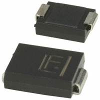
DO-214AB (SMC J-Bend)
0.126 (3.20) 0.114 (2.90)
Stand-off Voltage 5.0 to 188V Peak Pulse Power 1500W
Cathode Band
0.245 (6.22) 0.220 (5.59)
ded ge xten Ran Ee g olta V
0.121 MIN. (3.07 MIN.)
Mounting Pad Layout
0.185 MAX. (4.69 MAX.)
0.280 (7.11) 0.260 (6.60) 0.012 (0.305) 0.006 (0.152) 0.103 (2.62) 0.079 (2.06) 0.060 (1.52) 0.030 (0.76) 0.320 (8.13) 0.305 (7.75)
0.060 MIN. (1.52 MIN.)
0.008 (0.203) Max.
Dimensions in inches and (millimeters)
0.320 REF
Features
• Underwriters Laboratory Recognition under UL standard for safety 497B: Isolated Loop Circuit Protection • Low profile package with built-in strain relief for surface mounted applications • Glass passivated junction • Low incremental surge resistance, excellent clamping capability • 1500W peak pulse power capability with a 10/1000µs waveform, repetition rate (duty cycle): 0.01% • Very fast response time • High temperature soldering guaranteed: 250°C/10 seconds at terminals
Mechanical Data
Case: JEDEC DO-214AB molded plastic over passivated junction Terminals: Solder plated, solderable per MIL-STD-750, Method 2026 Polarity: For unidirectional types the band denotes the cathode, which is positive with respect to the anode under normal TVS operation Weight: 0.007 oz., 0.21 g Flammability: Epoxy is rated UL 94V-0 Packaging Codes – Options (Antistatic): 51 – 1K per Bulk box, 10K/carton 57 – 850 per 7" plastic Reel (16mm tape), 8.5K/carton 9A – 3.5K per 13" plastic Reel (16mm tape), 35K/carton
Devices for Bidirectional Applications
For bi-directional devices, use suffix C or CA (e.g. SMCJ10C, SMCJ10CA). Electrical characteristics apply in both directions.
Maximum Ratings & Thermal Characteristics
Parameter Peak pulse power dissipation with a 10/1000µs waveform(1)(2) Peak pulse current with a 10/1000µs waveform(1) Peak forward surge current 8.3ms single half sine-wave uni-directional only Typical thermal resistance, junction to ambient (3) Typical thermal resistance, junction to lead Operating junction and storage temperature range
(2)
Ratings at 25°C ambient temperature unless otherwise specified.
Symbol PPPM IPPM IFSM RθJA RθJL TJ, TSTG
Value Minimum 1500 See Next Table 200 75 15 – 55 to +150
Unit W A A °C/W °C/W °C
Notes: (1) Non-repetitive current pulse, per Fig.3 and derated above TA = 25°C per Fig. 2 (2) Mounted on 0.31 x 0.31” (8.0 x 8.0mm) copper pads to each terminal (3) Mounted on minimum recommended pad layout
Document Number 88394 26-Sep-02
www.vishay.com 1
�SMCJ5.0 thru 188CA
Vishay Semiconductors
formerly General Semiconductor
Electrical Characteristics Ratings at 25°C ambient temperature unless otherwise specified. V
Device Type Modified “J” Bend Lead +SMCJ5.0 +SMCJ5.0A(5) +SMCJ6.0 +SMCJ6.0A +SMCJ6.5 +SMCJ6.5A +SMCJ7.0 +SMCJ7.0A +SMCJ7.5 +SMCJ7.5A +SMCJ8.0 +SMCJ8.0A +SMCJ8.5 +SMCJ8.5A +SMCJ9.0 +SMCJ9.0A +SMCJ10 +SMCJ10A +SMCJ11 +SMCJ11A +SMCJ12 +SMCJ12A +SMCJ13 +SMCJ13A +SMCJ14 +SMCJ14A +SMCJ15 +SMCJ15A +SMCJ16 +SMCJ16A +SMCJ17 +SMCJ17A +SMCJ18 +SMCJ18A +SMCJ20 +SMCJ20A +SMCJ22 +SMCJ22A +SMCJ24 +SMCJ24A +SMCJ26 +SMCJ26A +SMCJ28 +SMCJ28A +SMCJ30 +SMCJ30A Device Marking Code UNI BI GDD GDD GDE GDE GDF GDF GDG GDG GDH BDH GDK BDK GDL GDL GDM GDM GDN BDN GDP BDP GDQ BDG GDR BDR GDS BDS GDT BDT GDU BDU GDV BDV GDW BDW GDX BDX GDY GDY GDZ GDZ GED BED GEE BEE GEF GEF GEG GEG GEH BEH GEK BEK GEL BEL GEM BEM GEN GEN GEP GEP GEQ GEQ GER GER GES BES GET BET GEU BEU GEV BEV GEW BEW GEX BEX GEY BEY GEZ BEZ GFD BFD GFE BFE GFF BFF GFG BFG GFH BFH GFK BFK Breakdown Voltage V(BR) at IT (1) (V) Min Max 6.40 7.82 6.40 7.07 6.67 8.15 6.67 7.37 7.22 8.82 7.22 7.98 7.78 9.51 7.78 8.60 8.33 10.2 8.33 9.21 8.89 10.9 8.89 9.83 9.44 11.5 9.44 10.4 10.0 12.2 10.0 11.1 11.1 13.6 11.1 12.3 12.2 14.9 12.2 13.5 13.3 16.3 13.3 14.7 14.4 17.6 14.4 15.9 15.6 19.1 15.6 17.2 16.7 20.4 16.7 18.5 17.8 21.8 17.8 19.7 18.9 23.1 18.9 20.9 20.0 24.4 20.0 22.1 22.2 27.1 22.2 24.5 24.4 29.8 24.4 26.9 26.7 32.6 26.7 29.5 28.9 35.3 28.9 31.9 31.1 38.0 31.1 34.4 33.3 40.7 33.3 36.8 Test Current IT (mA) 10.0 10.0 10.0 10.0 10.0 10.0 10.0 10.0 1.0 1.0 1.0 1.0 1.0 1.0 1.0 1.0 1.0 1.0 1.0 1.0 1.0 1.0 1.0 1.0 1.0 1.0 1.0 1.0 1.0 1.0 1.0 1.0 1.0 1.0 1.0 1.0 1.0 1.0 1.0 1.0 1.0 1.0 1.0 1.0 1.0 1.0 Stand-off Voltage VWM (V) 5.0 5.0 6.0 6.0 6.5 6.5 7.0 7.0 7.5 7.5 8.0 8.0 8.5 8.5 9.0 9.0 10 10 11 11 12 12 13 13 14 14 15 15 16 16 17 17 18 18 20 20 22 22 24 24 26 26 28 28 30 30
F
= 3.5V at IF = 100A (uni-directional only)
Maximum Maximum Maximum Reverse Leakage Peak Pulse Surge Clamping at VWM Current IPPM Voltage at IPPM ID (µA) (3) (A)(2) VC (V) 1000 156.3 9.6 1000 163.0 9.2 1000 131.6 11.4 1000 145.6 10.3 500 122.0 12.3 500 133.9 11.2 200 112.8 13.3 200 125.0 12.0 100 104.9 14.3 100 116.3 12.9 50 100.0 15.0 50 110.3 13.6 20 94.3 15.9 20 104.2 14.4 10 88.8 16.9 10 97.4 15.4 5.0 79.8 18.8 5.0 88.2 17.0 5.0 74.6 20.1 5.0 82.4 18.2 5.0 68.2 22.0 5.0 75.4 19.9 1.0 63.0 23.8 1.0 69.8 21.5 1.0 58.1 25.8 1.0 64.7 23.2 1.0 55.8 26.9 1.0 61.5 24.4 1.0 52.1 28.8 1.0 57.7 26.0 1.0 49.2 30.5 1.0 54.3 27.6 1.0 46.6 32.2 1.0 51.4 29.2 1.0 41.9 35.8 1.0 46.3 32.4 1.0 38.1 39.4 1.0 42.3 35.5 1.0 34.9 43.0 1.0 38.6 38.9 1.0 32.2 46.6 1.0 35.6 42.1 1.0 30.0 50.0 1.0 33.0 45.4 1.0 28.0 53.5 1.0 31.0 48.4
Notes: (1) Pulse test: tp ≤ 50ms (2) Surge current waveform per Fig. 3 and derate per Fig. 2 (3) For bi-directional types having VWM of 10 Volts and less, the ID limit is doubled (4) All terms and symbols are consistent with ANSI/IEEE C62.35 (5) For the bi-directional SMCG/SMCJ5.0CA, the maximum V(BR) is 7.25V + Underwriters Laboratory Recognition for the classification of protectors (QVGQ2) under the UL standard for safety 497B and file number E136766 for both uni-directional and bi-directional devices
www.vishay.com 2
Document Number 88394 26-Sep-02
�SMCJ5.0 thru 188CA
Vishay Semiconductors
formerly General Semiconductor
Electrical Characteristics Ratings at 25°C ambient temperature unless otherwise specified. V
Device Type Modified “J” Bend Lead +SMCJ33 +SMCJ33A +SMCJ36 +SMCJ36A +SMCJ40 +SMCJ40A +SMCJ43 +SMCJ43A +SMCJ45 +SMCJ45A +SMCJ48 +SMCJ48A +SMCJ51 +SMCJ51A +SMCJ54 +SMCJ54A +SMCJ58 +SMCJ58A +SMCJ60 +SMCJ60A +SMCJ64 +SMCJ64A +SMCJ70 +SMCJ70A +SMCJ75 +SMCJ75A +SMCJ78 +SMCJ78A +SMCJ85 +SMCJ85A +SMCJ90 +SMCJ90A +SMCJ100 +SMCJ100A +SMCJ110 +SMCJ110A +SMCJ120 +SMCJ120A +SMCJ130 +SMCJ130A +SMCJ150 +SMCJ150A +SMCJ160 +SMCJ160A +SMCJ170 +SMCJ170A SMCJ188 SMCJ188A Device Marking Code UNI BI GFL BFL GFM BFM GFN BFN GFP BFP GFQ BFQ GFR BFR GFS BFS GFT BFT GFU GFU GFV GFV GFW GFW GFX GFX GFY GFY GFZ GFZ GGD GGD GGE GGE GGF GGF GGG GGG GGH GGH GGK GGK GGL GGL GGM GGM GGN GGN GGP GGP GGQ GGQ GGR GGR GGS GGS GGT GGT GGU GGU GGV GGV GGW GGW GGX GGX GGY GGY GGZ GGZ GHD GHD GHE GHE GHF GHF GHG GHG GHH GHH GHK GHK GHL GHL GHM GHM GHN GHN GHP GHP GHQ GHQ GHR GHR GHT GHT GHS GHS Breakdown Voltage V(BR) at IT (1) (V) Min Max 36.7 44.9 36.7 40.6 40.0 48.9 40.0 44.2 44.4 54.3 44.4 49.1 47.8 58.4 47.8 52.8 50.0 61.1 50.0 55.3 53.3 65.1 53.3 58.9 56.7 69.3 56.7 62.7 60.0 73.3 60.0 66.3 64.4 78.7 64.4 71.2 66.7 81.5 66.7 73.7 71.1 86.9 71.1 78.6 77.8 95.1 77.8 86.0 83.3 102 83.3 92.1 86.7 106 86.7 95.8 94.4 115 94.4 104 100 122 100 111 111 136 111 123 122 149 122 135 133 163 133 147 144 176 144 159 167 204 167 185 178 218 178 197 189 231 189 209 209 255 209 231 Test Current IT (mA) 1.0 1.0 1.0 1.0 1.0 1.0 1.0 1.0 1.0 1.0 1.0 1.0 1.0 1.0 1.0 1.0 1.0 1.0 1.0 1.0 1.0 1.0 1.0 1.0 1.0 1.0 1.0 1.0 1.0 1.0 1.0 1.0 1.0 1.0 1.0 1.0 1.0 1.0 1.0 1.0 1.0 1.0 1.0 1.0 1.0 1.0 1.0 1.0 Stand-off Voltage VWM (V) 33 33 36 36 40 40 43 43 45 45 48 48 51 51 54 54 58 58 60 60 64 64 70 70 75 75 78 78 85 85 90 90 100 100 110 110 120 120 130 130 150 150 160 160 170 170 188 188
F
= 3.5V at IF = 100A (uni-directional only)
Maximum Maximum Maximum Reverse Leakage Peak Pulse Surge Clamping at VWM Current IPPM Voltage at IPPM ID (µA) (3) (A)(2) VC (V) 1.0 25.4 59.0 1.0 28.1 53.3 1.0 23.3 64.3 1.0 25.8 58.1 1.0 21.0 71.4 1.0 23.3 64.5 1.0 19.6 76.7 1.0 21.6 69.4 1.0 18.7 80.3 1.0 20.6 72.7 1.0 17.5 85.5 1.0 19.4 77.4 1.0 16.5 91.1 1.0 18.2 82.4 1.0 15.6 96.3 1.0 17.2 87.1 1.0 14.6 103 1.0 16.0 93 1.0 14.0 107 1.0 15.5 96 1.0 13.2 114 1.0 14.6 103 1.0 12.0 125 1.0 13.3 113 1.0 11.2 134 1.0 12.4 121 1.0 10.8 139 1.0 11.9 126 1.0 9.9 151 1.0 10.9 137 1.0 9.4 160 1.0 10.3 146 1.0 8.4 179 1.0 9.3 162 1.0 7.7 196 1.0 8.5 177 1.0 7.0 214 1.0 7.8 193 1.0 6.5 231 1.0 7.2 209 1.0 5.6 268 1.0 6.2 243 1.0 5.2 287 1.0 5.8 259 1.0 4.9 304 1.0 5.5 275 1.0 4.4 344 1.0 4.6 328
Notes: (1) Pulse test: tp ≤ 50ms (2) Surge current waveform per Fig. 3 and derate per Fig. 2 (3) For bi-directional types having VWM of 10 Volts and less, the ID limit is doubled (4) All terms and symbols are consistent with ANSI/IEEE C62.35 + Underwriters Laboratory Recognition for the classification of protectors (QVGQ2) under the UL standard for safety 497B and file number E136766 for both uni-directional and bi-directional devices
Document Number 88394 26-Sep-02
www.vishay.com 3
�SMCJ5.0 thru 188CA
Vishay Semiconductors
formerly General Semiconductor
Ratings and Characteristic Curves (TA = 25°C unless otherwise noted)
Fig. 1 – Peak Pulse Power Rating Curve
Peak Pulse Power (PPP) or Current (IPP) Derating in Percentage, %
100 100
Fig. 2 – Pulse Derating Curve
PPPM — Peak Pulse Power (kW)
75
10
50
1 0.31 x 0.31" (8.0 x 8.0mm) Copper Pad Areas 0.1 0.1µs 1.0µs 10µs 100µs 1.0ms 10ms
25
0
0
25
50
75
100
125
150
175
200
td — Pulse Width (sec.)
TA — Ambient Temperature (°C)
Fig. 3 – Pulse Waveform
150
Fig. 4 – Typical Junction Capacitance Uni-Directional
20,000
IPPM — Peak Pulse Current, % IRSM
100
Peak Value IPPM
CJ — Junction Capacitance (pF)
tr = 10µsec.
TJ = 25°C Pulse Width (td) is defined as the point where the peak current decays to 50% of IPPM
10,000
Measured at Zero Bias
1,000 VR, Measured at Stand-Off Voltage, VWM 100 Uni-Directional Bi-Directional 10 TJ = 25°C f = 1.0MHz Vsig = 50mVp-p 100 400
Half Value — IPP 2 IPPM 50 10/1000µsec. Waveform as defined by R.E.A.
td 0 0 1.0 2.0 3.0 4.0 1 10
t — Time (ms)
VWM — Reverse Stand-Off Voltage (V)
Fig. 5 – Typical Transient Thermal Impedance
100
Fig. 6 - Maximum Non-Repetitive Forward Surge Current Uni-Directional Use Only
200
Transient Thermal Impedance (°C/W)
10
1.0
Peak Forward Surge Current, Amperes
100
0.1 0.001
10
0.01 0.1 1 10 100 1000
8.3ms Single Half Sine-Wave (JEDEC Method) TJ = TJ max.
1
10
100
tp — Pulse Duration (sec) www.vishay.com 4
Number of Cycles at 60Hz Document Number 88394 26-Sep-02
�
很抱歉,暂时无法提供与“SMCJ100C”相匹配的价格&库存,您可以联系我们找货
免费人工找货- 国内价格
- 1+0.5922
- 100+0.5502
- 300+0.5082
- 500+0.4662
- 2000+0.4452
- 5000+0.4326
- 国内价格
- 1+0.4275
- 100+0.399
- 300+0.3705
- 500+0.342
- 2000+0.32775
- 5000+0.3192
- 国内价格
- 1+0.63352
- 10+0.57337
- 30+0.53327
- 100+0.47312
- 500+0.44505
- 1000+0.425
- 国内价格
- 1+2.21111
- 30+2.13486
- 100+1.98237
- 500+1.82988
- 1000+1.75364


 工商网监
湘ICP备2023018690号
工商网监
湘ICP备2023018690号
