DS1302
DS1302 Trickle Charge Timekeeping Chip
FEATURES
�
PIN ASSIGNMENT
Real time clock counts seconds, minutes
hours, date of the month, month, day of the
week, and year with leap year compensation
valid up to 2100
31 x 8 RAM for scratchpad data storage
Serial I/O for minimum pin count
2.0–5.5V full operation
Uses less than 300 nA at 2.0V
Single–byte or multiple–byte (burst mode)
data transfer for read or write of clock or
RAM data
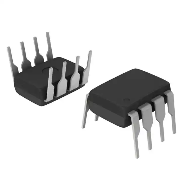
8–pin DIP or optional 8–pin SOICs for
surface mount
Simple 3–wire interface
TTL–compatible (VCC = 5V)
Optional industrial temperature range
–40°C to +85°C
DS1202 compatible
Recognized by Underwriters Laboratory
�
�
�
�
�
�
�
�
�
�
�
VCC2
1
8
VCC1
X1
2
7
SCLK
X2
3
6
I/O
GND
4
5
RST
DS1302
8-Pin DIP (300 mil)
VCC2
1
8
VCC1
X1
2
7
SCLK
X2
3
6
I/O
GND
4
5
RST
DS1302Z 8-Pin SOIC (150 mil)
PIN DESCRIPTION
X1, X2
GND
RST
I/O
SCLK
VCC1, VCC2
– 32.768 kHz Crystal Pins
– Ground
– Reset
– Data Input/Output
– Serial Clock
– Power Supply Pins
DESCRIPTION
The DS1302 Trickle Charge Timekeeping Chip contains a real time clock/calendar and 31 bytes of static
RAM. It communicates with a microprocessor via a simple serial interface. The real time clock/calendar
provides seconds, minutes, hours, day, date, month, and year information. The end of the month date is
automatically adjusted for months with less than 31 days, including corrections for leap year. The clock
operates in either the 24–hour or 12–hour format with an AM/PM indicator.
http://www.hgsemi.com.cn
1
2018 AUG
�DS1302
Interfacing the DS1302 with a microprocessor is simplified by using synchronous serial communication.
Only three wires are required to communicate with the clock/RAM: (1) RST (Reset), (2) I/O (Data line),
and (3) SCLK (Serial clock). Data can be transferred to and from the clock/RAM 1 byte at a time or in a
burst of up to 31 bytes. The DS1302 is designed to operate on very low power and retain data and clock
information on less than 1 microwatt.
The DS1302 is the successor to the DS1202. In addition to the basic timekeeping functions of the
DS1202, the DS1302 has the additional features of dual power pins for primary and back–up power
supplies, programmable trickle charger for VCC1, and seven additional bytes of scratchpad memory.
OPERATION
The main elements of the Serial Timekeeper are shown in Figure 1: shift register, control logic, oscillator,
real time clock, and RAM.
DS1302 BLOCK DIAGRAM Figure 1
SIGNAL DESCRIPTIONS
VCC1 – VCC1 provides low power operation in single supply and battery operated systems as well as low
power battery backup. In systems using the trickle charger, the rechargeable energy source is connected
to this pin.
VCC2 – Vcc2 is the primary power supply pin in a dual supply configuration. VCC1 is connected to a
backup source to maintain the time and date in the absence of primary power.
The DS1302 will operate from the larger of VCC1 or VCC2. When VCC2 is greater than VCC1 + 0.2V, VCC2
will power the DS1302. When VCC2 is less than VCC1, VCC1 will power the DS1302.
SCLK (Serial Clock Input) – SCLK is used to synchronize data movement on the serial interface.
I/O (Data Input/Output) – The I/O pin is the bi-directional data pin for the 3-wire interface.
RST (Reset) – The reset signal must be asserted high during a read or a write.
http://www.hgsemi.com.cn
2
2018 AUG
�DS1302
X1, X2 – Connections for a standard 32.768 kHz quartz crystal. The internal oscillator is designed for
operation with a crystal having a specified load capacitance of 6 pF. For more information on crystal
selection and crystal layout considerations, please consult Application Note 58, “Crystal Considerations
with Dallas Real Time Clocks.” The DS1302 can also be driven by an external 32.768 kHz oscillator. In
this configuration, the X1 pin is connected to the external oscillator signal and the X2 pin is floated.
COMMAND BYTE
The command byte is shown in Figure 2. Each data transfer is initiated by a command byte. The MSB
(Bit 7) must be a logic 1. If it is 0, writes to the DS1302 will be disabled. Bit 6 specifies clock/calendar
data if logic 0 or RAM data if logic 1. Bits 1 through 5 specify the designated registers to be input or
output, and the LSB (bit 0) specifies a write operation (input) if logic 0 or read operation (output) if logic
1. The command byte is always input starting with the LSB (bit 0).
ADDRESS/COMMAND BYTE Figure 2
RESET AND CLOCK CONTROL
All data transfers are initiated by driving the RST input high. The RST input serves two functions. First,
RST turns on the control logic which allows access to the shift register for the address/command
sequence. Second, the RST signal provides a method of terminating either single byte or multiple byte
data transfer.
A clock cycle is a sequence of a falling edge followed by a rising edge. For data inputs, data must be
valid during the rising edge of the clock and data bits are output on the falling edge of clock. If the RST
input is low all data transfer terminates and the I/O pin goes to a high impedance state. Data transfer is
illustrated in Figure 3. At power–up, RST must be a logic 0 until VCC > 2.0 volts. Also SCLK must be at
a logic 0 when RST is driven to a logic 1 state.
DATA INPUT
Following the eight SCLK cycles that input a write command byte, a data byte is input on the rising edge
of the next eight SCLK cycles. Additional SCLK cycles are ignored should they inadvertently occur.
Data is input starting with bit 0.
DATA OUTPUT
Following the eight SCLK cycles that input a read command byte, a data byte is output on the falling
edge of the next eight SCLK cycles. Note that the first data bit to be transmitted occurs on the first falling
edge after the last bit of the command byte is written. Additional SCLK cycles retransmit the data bytes
should they inadvertently occur so long as RST remains high. This operation permits continuous burst
mode read capability. Also, the I/O pin is tri–stated upon each rising edge of SCLK. Data is output
starting with bit 0.
BURST MODE
Burst mode may be specified for either the clock/calendar or the RAM registers by addressing location 31
decimal (address/command bits 1 through 5 = logic 1). As before, bit 6 specifies clock or RAM and bit 0
http://www.hgsemi.com.cn
3
2018 AUG
�DS1302
specifies read or write. There is no data storage capacity at locations 9 through 31 in the Clock/Calendar
Registers or location 31 in the RAM registers. Reads or writes in burst mode start with bit 0 of address 0.
When writing to the clock registers in the burst mode, the first eight registers must be written in order for
the data to be transferred. However, when writing to RAM in burst mode it is not necessary to write all
31 bytes for the data to transfer. Each byte that is written to will be transferred to RAM regardless of
whether all 31 bytes are written or not.
CLOCK/CALENDAR
The clock/calendar is contained in seven write/read registers as shown in Figure 4. Data contained in the
clock/ calendar registers is in binary coded decimal format (BCD).
CLOCK HALT FLAG
Bit 7 of the seconds register is defined as the clock halt flag. When this bit is set to logic 1, the clock
oscillator is stopped and the DS1302 is placed into a low–power standby mode with a current drain of less
than 100 nanoamps. When this bit is written to logic 0, the clock will start. The initial power on state is
not defined.
AM-PM/12-24 MODE
Bit 7 of the hours register is defined as the 12– or 24–hour mode select bit. When high, the 12–hour
mode is selected. In the 12–hour mode, bit 5 is the AM/PM bit with logic high being PM. In the 24–hour
mode, bit 5 is the second 10-hour bit (20 – 23 hours).
WRITE PROTECT BIT
Bit 7 of the control register is the write-protect bit. The first seven bits (bits 0 – 6) are forced to 0 and
will always read a 0 when read. Before any write operation to the clock or RAM, bit 7 must be 0. When
high, the write protect bit prevents a write operation to any other register. The initial power on state is not
defined. Therefore the WP bit should be cleared before attempting to write to the device.
TRICKLE CHARGE REGISTER
This register controls the trickle charge characteristics of the DS1302. The simplified schematic of
Figure 5 shows the basic components of the trickle charger. The trickle charge select (TCS) bits (bits
4 -7) control the selection of the trickle charger. In order to prevent accidental enabling, only a pattern of
1010 will enable the trickle charger. All other patterns will disable the trickle charger. The DS1302
powers up with the trickle charger disabled. The diode select (DS) bits (bits 2 – 3) select whether one
diode or two diodes are connected between VCC2 and VCC1. If DS is 01, one diode is selected or if DS is
10, two diodes are selected. If DS is 00 or 11, the trickle charger is disabled independently of TCS. The
RS bits (bits 0 -1) select the resistor that is connected between VCC2 and VCC1. The resistor selected by
the resistor select (RS) bits is as follows:
RS Bits
00
01
10
11
Resistor
None
R1
R2
R3
Typical Value
None
2 kΩ
4 kΩ
8 kΩ
If RS is 00, the trickle charger is disabled independently of TCS.
http://www.hgsemi.com.cn
4
2018 AUG
�DS1302
Diode and resistor selection is determined by the user according to the maximum current desired for
battery or super cap charging. The maximum charging current can be calculated as illustrated in the
following example. Assume that a system power supply of 5 volt is applied to VCC2 and a super cap is
connected to VCC1. Also assume that the trickle charger has been enabled with one diode and resistor R1
between VCC2 and VCC1. The maximum current Imax would therefore be calculated as follows:
Imax = (5.0V – diode drop) / R1
~ (5.0V – 0.7V) / 2 kΩ
~ 2.2 mA
Obviously, as the super cap charges, the voltage drop between VCC2 and VCC1 will decrease and therefore
the charge current will decrease.
CLOCK/CALENDAR BURST MODE
The clock/calendar command byte specifies burst mode operation. In this mode the first eight
clock/calendar registers can be consecutively read or written (see Figure 4) starting with bit 0 of address
0.
If the write protect bit is set high when a write clock/calendar burst mode is specified, no data transfer
will occur to any of the eight clock/calendar registers (this includes the control register). The trickle
charger is not accessible in burst mode.
At the beginning of a clock burst read, the current time is transferred to a second set of registers. The
time information is read from these secondary registers, while the clock may continue to run. This
eliminates the need to re-read the registers in case of an update of the main registers during a read.
RAM
The static RAM is 31 x 8 bytes addressed consecutively in the RAM address space.
RAM BURST MODE
The RAM command byte specifies burst mode operation. In this mode, the 31 RAM registers can be
consecutively read or written (see Figure 4) starting with bit 0 of address 0.
REGISTER SUMMARY
A register data format summary is shown in Figure 4.
CRYSTAL SELECTION
A 32.768 kHz crystal can be directly connected to the DS1302 via X1 and X2. The crystal selected for
use should have a specified load capacitance (CL) of 6 pF. For more information on crystal selection and
crystal layout consideration, please consult Application Note 58, “Crystal Considerations with Dallas
Real Time Clocks."
http://www.hgsemi.com.cn
5
2018 AUG
�DS1302
DATA TRANSFER SUMMARY Figure 3
SINGLE BYTE READ
RST
SCLK
I/O
R/ W
A0
A1
A2
A3
A4 R/C 1
SINGLE BYTE WRITE
RST
SCLK
I/O
R/ W
A0
A1
A2
A3
A4 R/C 1
D0
D1
D2
D3
D4
D5
D6 D7
In burst mode, RST is kept high and additional SCLK cycles are sent until the end of the burst.
http://www.hgsemi.com.cn
6
2018 AUG
�DS1302
REGISTER ADDRESS/DEFINITION Figure 4
http://www.hgsemi.com.cn
7
2018 AUG
�DS1302
DS1302 PROGRAMMABLE TRICKLE CHARGER Figure 5
http://www.hgsemi.com.cn
8
2018 AUG
�


 工商网监
湘ICP备2023018690号
工商网监
湘ICP备2023018690号

