74LVC1GU04
Unbuffered inverter
Rev. 13 — 12 December 2016
Product data sheet
1. General description
The 74LVC1GU04 is a single unbuffered inverter.
The input can be driven from either 3.3 V or 5 V devices. This feature allows the use of
this device in a mixed 3.3 V and 5 V environment.
2. Features and benefits
Wide supply voltage range from 1.65 V to 5.5 V
High noise immunity
ESD protection:
HBM JESD22-A114F exceeds 2000 V
MM JESD22-A115-A exceeds 200 V
24 mA output drive (VCC = 3.0 V)
CMOS low power consumption
Latch-up performance exceeds 250 mA
Input accepts voltages up to 5 V
Multiple package options
Specified from 40 C to +85 C and 40 C to +125 C
3. Ordering information
Table 1.
Ordering information
Type number
Package
Temperature range
Name
Description
Version
74LVC1GU04GW
40 C to +125 C
TSSOP5
plastic thin shrink small outline package;
5 leads; body width 1.25 mm
SOT353-1
74LVC1GU04GV
40 C to +125 C
SC-74A
plastic surface-mounted package; 5 leads
SOT753
74LVC1GU04GM
40 C to +125 C
XSON6
plastic extremely thin small outline package;
no leads; 6 terminals; body 1 1.45 0.5 mm
SOT886
74LVC1GU04GF
40 C to +125 C
XSON6
plastic extremely thin small outline package;
no leads; 6 terminals; body 1 1 0.5 mm
SOT891
74LVC1GU04GN
40 C to +125 C
XSON6
extremely thin small outline package; no leads; SOT1115
6 terminals; body 0.9 1.0 0.35 mm
74LVC1GU04GS
40 C to +125 C
XSON6
extremely thin small outline package; no leads; SOT1202
6 terminals; body 1.0 1.0 0.35 mm
74LVC1GU04GX
40 C to +125 C
X2SON5
X2SON5: plastic thermal enhanced extremely
thin small outline package; no leads;
5 terminals; body 0.8 0.8 0.35 mm
SOT1226
�74LVC1GU04
Nexperia
Unbuffered inverter
4. Marking
Table 2.
Marking codes
Type number
Marking[1]
74LVC1GU04GW
VD
74LVC1GU04GV
VU4
74LVC1GU04GM
VD
74LVC1GU04GF
VD
74LVC1GU04GN
VD
74LVC1GU04GS
VD
74LVC1GU04GX
VD
[1]
The pin 1 indicator is located on the lower left corner of the device, below the marking code.
5. Functional diagram
9&&
����ȍ
$
�
$
<
�
�
PQD���
Fig 1.
�
<
�
PQD���
Logic symbol
Fig 2.
9&&
PQD���
IEC logic symbol
Fig 3.
Logic diagram
6. Pinning information
6.1 Pinning
��/9&�*8��
��/9&�*8��
Q�F�
�
$
�
*1'
�
�
�
Q�F�
�
�
9&&
$
�
�
Q�F�
*1'
�
�
<
9&&
<
���DDE���
7UDQVSDUHQW�WRS�YLHZ
���DDE���
Fig 4.
Pin configuration SOT353-1 and SOT753
74LVC1GU04
Product data sheet
Fig 5.
Pin configuration SOT886
All information provided in this document is subject to legal disclaimers.
Rev. 13 — 12 December 2016
©
Nexperia B.V. 2017. All rights reserved
2 of 20
�74LVC1GU04
Nexperia
Unbuffered inverter
��/9&�*��
��/9&�*8��
Q�F�
Q�F�
�
�
9&&
$
�
�
Q�F�
*1'
�
�
<
�
9&&
�
<
�
*1'
$
���DDI���
�
DDD�������
7UDQVSDUHQW�WRS�YLHZ
7UDQVSDUHQW�WRS�YLHZ
Fig 6.
�
Pin configuration SOT891, SOT1115 and
SOT1202
Fig 7.
Pin configuration SOT1226 (X2SON5)
6.2 Pin description
Table 3.
Pin description
Symbol
Pin
Description
TSSOP5, SC-74A and X2SON5
XSON6
n.c.
1
1
not connected
A
2
2
data input
GND
3
3
ground (0 V)
Y
4
4
data output
n.c.
-
5
not connected
VCC
5
6
supply voltage
7. Functional description
Table 4.
Function table[1]
Input (A)
Output (Y)
L
H
H
L
[1]
H = HIGH voltage level; L = LOW voltage level.
74LVC1GU04
Product data sheet
All information provided in this document is subject to legal disclaimers.
Rev. 13 — 12 December 2016
©
Nexperia B.V. 2017. All rights reserved
3 of 20
�74LVC1GU04
Nexperia
Unbuffered inverter
8. Limiting values
Table 5.
Limiting values
In accordance with the Absolute Maximum Rating System (IEC 60134). Voltages are referenced to GND (ground = 0 V).
Symbol
Parameter
VCC
supply voltage
IIK
input clamping current
VI
input voltage
IOK
output clamping current
Conditions
[1]
Active mode
VO = 0 V to VCC
output current
supply current
IGND
ground current
Ptot
total power dissipation
Tstg
storage temperature
Unit
0.5
+6.5
V
-
50
mA
0.5
+6.5
V
-
50
mA
0.5
VCC + 0.5
VO > VCC or VO < 0 V
output voltage
IO
Max
VI < 0 V
VO
ICC
Min
[1][2]
Tamb = 40 C to +125 C
-
50
mA
-
+100
mA
-
100
mA
-
250
mW
65
+150
C
[3]
[1]
The input and output voltage ratings may be exceeded if the input and output current ratings are observed.
[2]
When VCC = 0 V (Power-down mode), the output voltage can be 5.5 V in normal operation.
[3]
V
For TSSOP5 and SC-74A packages: above 87.5 C the value of Ptot derates linearly with 4.0 mW/K.
For XSON6 and X2SON5 packages: above 118 C the value of Ptot derates linearly with 7.8 mW/K.
9. Recommended operating conditions
Table 6.
Recommended operating conditions
Voltages are referenced to GND (ground = 0 V).
Symbol Parameter
VCC
supply voltage
VI
input voltage
VO
output voltage
Tamb
ambient temperature
t/V
input transition rise and fall rate
74LVC1GU04
Product data sheet
Conditions
Active mode
Min
Typ
Max
Unit
1.65
-
5.5
V
0
-
5.5
V
0
-
VCC
V
40
-
+125
C
VCC = 1.65 V to 2.7 V
0
-
20
ns/V
VCC = 2.7 V to 5.5 V
0
-
10
ns/V
All information provided in this document is subject to legal disclaimers.
Rev. 13 — 12 December 2016
©
Nexperia B.V. 2017. All rights reserved
4 of 20
�74LVC1GU04
Nexperia
Unbuffered inverter
10. Static characteristics
Table 7.
Static characteristics
At recommended operating conditions; voltages are referenced to GND (ground = 0 V).
Symbol Parameter
Conditions
Min
Typ[1]
Max
Unit
Tamb = 40 C to +85 C
VIH
HIGH-level input voltage
VCC = 1.65 V to 5.5 V
0.75 VCC
-
VIL
LOW-level input voltage
VCC = 1.65 V to 5.5 V
-
-
VOH
HIGH-level output voltage VI = VIH or VIL
VCC 0.1
-
-
V
IO = 4 mA; VCC = 1.65 V
1.2
-
-
V
IO = 8 mA; VCC = 2.3 V
1.9
-
-
V
IO = 12 mA; VCC = 2.7 V
2.2
-
-
V
IO = 24 mA; VCC = 3.0 V
2.3
-
-
V
IO = 32 mA; VCC = 4.5 V
3.8
-
-
V
IO = 100 A; VCC = 1.65 V to 5.5 V
-
-
0.1
V
IO = 4 mA; VCC = 1.65 V
-
-
0.45
V
IO = 100 A; VCC = 1.65 V to 5.5 V
VOL
LOW-level output voltage
-
V
0.25 VCC V
VI = VIH or VIL
IO = 8 mA; VCC = 2.3 V
-
-
0.3
V
IO = 12 mA; VCC = 2.7 V
-
-
0.4
V
IO = 24 mA; VCC = 3.0 V
-
-
0.55
V
IO = 32 mA; VCC = 4.5 V
-
-
0.55
V
II
input leakage current
VI = 5.5 V or GND; VCC = 0 V to 5.5 V
-
0.1
1
A
ICC
supply current
VI = 5.5 V or GND; IO = 0 A;
VCC = 1.65 V to 5.5 V
-
0.1
4
A
CI
input capacitance
VCC = 3.3 V; VI = GND to VCC
-
6
-
pF
-
V
Tamb = 40 C to +125 C
VIH
HIGH-level input voltage
VCC = 1.65 V to 5.5 V
0.8 VCC
-
VIL
LOW-level input voltage
VCC = 1.65 V to 5.5 V
-
-
VOH
HIGH-level output voltage VI = VIH or VIL
IO = 100 A; VCC = 1.65 V to 5.5 V
74LVC1GU04
Product data sheet
0.2 VCC V
VCC 0.1
-
-
V
IO = 4 mA; VCC = 1.65 V
0.95
-
-
V
IO = 8 mA; VCC = 2.3 V
1.7
-
-
V
IO = 12 mA; VCC = 2.7 V
1.9
-
-
V
IO = 24 mA; VCC = 3.0 V
2.0
-
-
V
IO = 32 mA; VCC = 4.5 V
3.4
-
-
V
All information provided in this document is subject to legal disclaimers.
Rev. 13 — 12 December 2016
©
Nexperia B.V. 2017. All rights reserved
5 of 20
�74LVC1GU04
Nexperia
Unbuffered inverter
Table 7.
Static characteristics …continued
At recommended operating conditions; voltages are referenced to GND (ground = 0 V).
Min
Typ[1]
Max
Unit
IO = 100 A; VCC = 1.65 V to 5.5 V
-
-
0.1
V
IO = 4 mA; VCC = 1.65 V
-
-
0.7
V
IO = 8 mA; VCC = 2.3 V
-
-
0.45
V
IO = 12 mA; VCC = 2.7 V
-
-
0.6
V
IO = 24 mA; VCC = 3.0 V
-
-
0.80
V
Symbol Parameter
Conditions
VOL
VI = VIH or VIL
LOW-level output voltage
-
-
0.80
V
II
input leakage current
VI = 5.5 V or GND; VCC = 0 V to 5.5 V
IO = 32 mA; VCC = 4.5 V
-
0.1
1
A
ICC
supply current
VI = 5.5 V or GND; IO = 0 A;
VCC = 1.65 V to 5.5 V
-
-
4
A
[1]
All typical values are measured at VCC = 3.3 V and Tamb = 25 C.
11. Dynamic characteristics
Table 8.
Dynamic characteristics
Voltages are referenced to GND (ground = 0 V). For test circuit see Figure 11.
Symbol Parameter
40 C to +85 C
Conditions
propagation delay A to Y; see Figure 8
tpd
[1]
Max
Min
Max
0.3
1.7
5.0
0.3
6.5
ns
VCC = 2.3 V to 2.7 V
0.3
1.3
4.0
0.3
5.5
ns
VCC = 2.7 V
0.5
1.7
5.0
0.5
6.5
ns
VCC = 3.0 V to 3.6 V
0.5
1.6
3.7
0.5
5.0
ns
0.5
1.3
3.0
0.5
4.0
ns
-
14.9
-
-
-
pF
VCC = 4.5 V to 5.5 V
power dissipation
capacitance
Typ[1]
[2]
VCC = 1.65 V to 1.95 V
CPD
40 C to +125 C Unit
Min
[3]
VI = GND to VCC;
VCC = 3.3 V
Typical values are measured at Tamb = 25 C and VCC = 1.8 V, 2.5 V, 2.7 V, 3.3 V and 5.0 V respectively.
[2]
tpd is the same as tPLH and tPHL.
[3]
CPD is used to determine the dynamic power dissipation (PD in W).
PD = CPD VCC2 fi N + (CL VCC2 fo) where:
fi = input frequency in MHz;
fo = output frequency in MHz;
CL = output load capacitance in pF;
VCC = supply voltage in V;
N = number of inputs switching;
(CL VCC2 fo) = sum of outputs.
74LVC1GU04
Product data sheet
All information provided in this document is subject to legal disclaimers.
Rev. 13 — 12 December 2016
©
Nexperia B.V. 2017. All rights reserved
6 of 20
�74LVC1GU04
Nexperia
Unbuffered inverter
12. Waveforms
9,
90
$�LQSXW
*1'
W 3+/
W 3/+
92+
90
很抱歉,暂时无法提供与“74LVC1GU04GM,115”相匹配的价格&库存,您可以联系我们找货
免费人工找货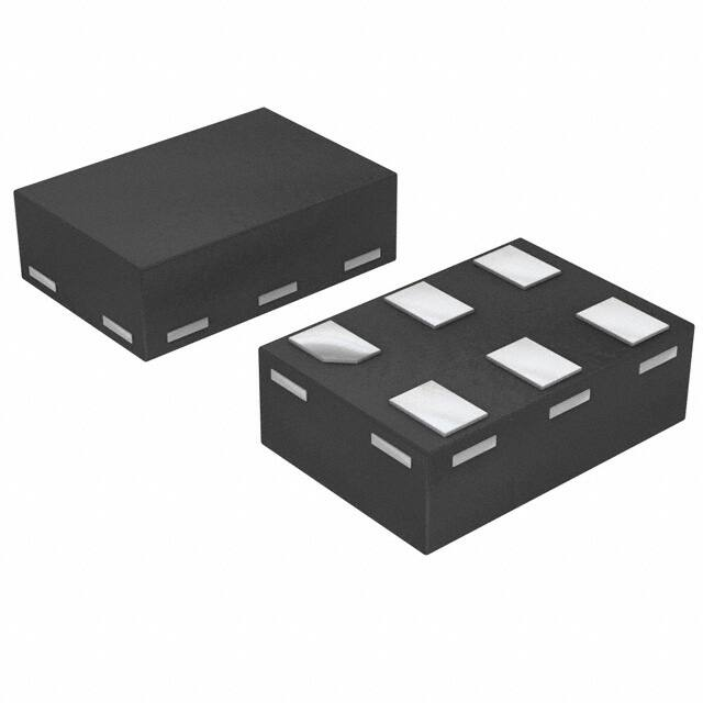


 工商网监
湘ICP备2023018690号
工商网监
湘ICP备2023018690号

