STC15W4K32S4 series MCU
Data Sheet
1
�CONTENTS
Chapter 1 General Overview of STC15W4K32S4 series..............12
1.1 Introduction of STC15W4K32S4 series MCU ................................. 12
1.2 Block diagram of STC15W4K32S4 series MCU ............................. 15
1.3 Pin Configurations of STC15W4K32S4 series MCU ...................... 16
1.4 STC15W4K32S4 series Selection and Price Table........................... 21
1.5 Naming rules of STC15W4K32S4 series MCU ............................... 22
1.6 Application Circuit Diagram for ISP of STC15W4K series .............. 23
1.6.1 Application Circuit Diagram for ISP using RS-232 Converter ................... 23
1.6.2 Application Circuit Diagram for ISP using USB to convert Serial Port ..... 24
1.6.3 Application Circuit Diagram for ISP directly using USB port.................... 25
——P3.0/P3.1 of STC15W4K series and IAP15W4K58S4 connect directly with D-/D+ of USB ......25
1.7 Pin Descriptions of STC15W4K32S4 series MCU .......................... 26
1.8 Package Dimension Drawings of STC15 series MCU ..................... 33
1.8.1 Dimension Drawings of DFN8..................................................................... 33
1.8.2 Dimension Drawings of SOP8 ..................................................................... 34
1.8.3 Dimension Drawings of DIP8 ...................................................................... 35
1.8.4 Dimension Drawings of SOP16 ................................................................... 36
1.8.5 Dimension Drawings of DIP16 .................................................................... 37
1.8.6 Dimension Drawings of SOP20 ................................................................... 38
1.8.7 Dimension Drawings of TSSOP20............................................................... 39
1.8.8 Dimension Drawings of LSSOP20............................................................... 40
1.8.9 Dimension Drawings of DIP20 .................................................................... 41
1.8.10 Dimension Drawings of SOP28 ................................................................. 42
1.8.11 Dimension Drawings of TSSOP28............................................................. 43
1.8.12 Dimension Drawings of SKDIP28 ............................................................. 44
1.8.13 Dimension Drawings of QFN28................................................................. 45
1.8.14 Dimension Drawings of LQFP32............................................................... 46
1.8.15 Dimension Drawings of SOP32 ................................................................. 47
1.8.16 Dimension Drawings of QFN32................................................................. 48
1.8.17 Dimension Drawings of PDIP40 ................................................................ 49
1.8.18 Dimension Drawings of LQFP44............................................................... 50
1.8.19 Dimension Drawings of PLCC44............................................................... 51
�1.8.20 Dimension Drawings of PQFP44 ............................................................... 52
1.8.21 Dimension Drawings of LQFP48............................................................... 53
1.8.22 Dimension Drawings of QFN48................................................................. 54
1.8.23 Dimension Drawings of LQFP64S............................................................. 55
1.8.24 Dimension Drawings of LQFP64L............................................................. 56
1.8.25 Dimension Drawings of QFN64................................................................. 57
1.9 Special Peripheral Function(CCP/SPI,UART1/2/3/4) Switch........... 58
1.9.1 Test Porgram that Switch CCP/PWM/PCA (C and ASM) .......................... 60
1.9.2 Test Porgram that Switch PWM2/3/4/5/PWMFLT (C and ASM)............... 62
1.9.3 Test Porgram that Switch PWM6/PWM7 (C and ASM).............................. 64
1.9.4 Test Porgram that Switch SPI (C and ASM) ............................................... 66
1.9.5 Test Porgram that Switch UART1 (C and ASM) ........................................68
1.9.6 Test Porgram that Switch UART2 (C and ASM) ........................................ 70
1.9.7 Test Porgram that Switch UART3 (C and ASM) ........................................ 72
1.9.8 Test Porgram that Switch UART4 (C and ASM) ........................................ 74
1.10 Global Unique Identification Number (ID) .................................... 76
Chapter 2 Clock, Reset and Power Management...........................81
2.1 Clock ................................................................................................. 81
2.1.1 On-Chip Configurable Clock ...................................................................... 81
2.1.2 Divider for System Clock............................................................................ 82
2.1.3 Programmable Clock Output (or as Frequency Divider) ............................ 83
2.1.3.1
2.1.3.2
2.1.3.3
2.1.3.4
2.1.3.5
2.1.3.6
2.1.3.7
Special Function Registers Related to Programmable Clock Output ..................83
Master Clock Output and Demo Program(C and ASM) ......................................88
Timer 0 Programmable Clock Output and Demo Program(C and ASM) ............91
Timer 1 Programmable Clock Output and Demo Program(C and ASM) ............95
Timer 2 Programmable Clock Output and Demo Program (C and ASM) ...........99
Timer 3 Programmable Clock Output and Demo Program (C and ASM) .........103
Timer 4 Programmable Clock Output and Demo Program (C and ASM) .........104
2.2 RESET Sources............................................................................... 105
2.2.1
2.2.2
2.2.3
2.2.4
2.2.5
2.2.6
2.2.7
2.2.8
External RST pin Reset ............................................................................. 105
Software Reset and Demo Program (C and ASM).................................... 106
Power-Off / Power-On Reset (POR) ......................................................... 109
MAX810 Speical Circuit Reset (Power-Off/ Power-On Reset Delay) ..... 109
Internal Low Voltage Detection Reset....................................................... 110
Watch-Dog-Timer Reset............................................................................ 113
Reset Caused by Program Accessing an Invalid Address ......................... 117
Warm Boot and Cold Boot Reset .............................................................. 118
�2.3 Power Management Modes..............................................................119
2.3.1 Slow Down Mode and Demo Program (C and ASM)............................... 120
2.3.2 Idle Mode and Demo Program (C and ASM)............................................ 123
2.2.3 Stop / Power Down (PD) Mode and Demo Program (C and ASM).......... 125
2.3.3.1
2.3.3.2
2.3.3.3
2.3.3.4
2.3.3.5
2.3.3.6
2.3.3.7
2.3.3.8
2.3.3.9
Demo Program Using Power-Down Wake-Up Timer to Wake Up Stop/PD Mode ....127
Demo Program Using External Interrupt INT0 to Wake Up Stop/PD Mode.....129
Demo Program Using External Interrupt INT1 to Wake Up Stop/PD Mode.....131
Demo Program Using External Interrupt INT2 to Wake Up Stop/PD Mode.....133
Demo Program Using External Interrupt INT3 to Wake Up Stop/PD Mode.....135
Demo Program Using External Interrupt INT4 to Wake Up Stop/PD Mode.....137
Program Using External Interrupt Extended by CCP/PCA to Wake Up PD Mode..139
Program Using the Level Change of RxD pin to Wake Up Stop/PD Mode.......143
Program Using the Level Change of RxD2 pin to Wake Up Stop/PD Mode.....147
Chapter 3 Memory Organization and SFRs.................................151
3.1 Program Memory ............................................................................ 151
3.2 Data Memory (SRAM) ................................................................... 152
3.2.1 On-chip Scratch-Pad RAM ....................................................................... 152
3.2.2 On-Chip Expanded RAM / XRAM /AUX-RAM...................................... 154
3.2.3 External Expandable 64KB RAM (Off-Chip RAM)................................. 160
3.3 Special Function Registers.............................................................. 163
3.3.1 Special Function Registers Address Map .................................................. 163
3.3.2 Special Function Registers Bits Description ............................................. 164
3.3.3 Dual Data Pointer Register (DPTR) .......................................................... 170
Chapter 4 Configurable I/O Ports of STC15 series MCU ...........171
4.1
4.2
4.3
4.4
4.5
4.6
4.7
I/O Ports Configurations ................................................................. 171
Special Explanation of P1.7/XTAL1 and P1.6/XTAL2 pin............ 174
Special Explanation of RST pin...................................................... 174
Special Explanation of RSTOUT_LOW pin .................................. 174
SFRs related to I/O ports and Its Address Statement...................... 175
Demo Program of STC15 series P0/P1/P2/P3/P4/P5 ..................... 179
I/O ports Modes .............................................................................. 185
4.7.1
4.7.2
4.7.3
4.7.4
Quasi-Bidirectional I/O ............................................................................. 185
Push-Pull Output ....................................................................................... 185
Input-Only (High-Impedance)Mode ......................................................... 186
Open-Drain Output.................................................................................... 186
�4.8 I/O Port Application Notes.............................................................. 186
4.9 Typical Transistor Control Circuit .................................................. 187
4.10 Typical Diode Control Circuit....................................................... 187
4.11 How to Make I/O Port Low after MCU Reset .............................. 187
4.12 Keyboard Scanning Circuit using I/O ports.................................. 188
4.13 Pin Function and Logic Turth Table of 74HC595......................... 189
4.14 Circuit Expanding I/O ports using 74HC595................................ 190
4.15 Circuit Driving 8-segment Digitron using 74HC595.................... 191
4.16 Demo Program of Driving 8-Segment Digitron ........................... 192
—— Using common I/O ports to Control 74HC595.................... 192
4.17 Application Circuit using A/D Conversion to Scan Key ............. 199
4.18 Demo Program using I/O ports to Simulate I2C Interface ............ 200
4.18.1 Master Mode using I/O ports to Simulate I2C Interface by Software ..... 200
4.18.2 Slave Mode using I/O ports to Simulate I2C Interface by Software........ 203
Chapter 5. Instruction System......................................................206
5.1 Addressing Modes........................................................................... 206
5.1.1
5.1.2
5.1.3
5.1.4
5.1.5
5.1.6
5.1.7
Immediate Addressing ............................................................................... 206
Direct Addressing ...................................................................................... 206
Indirect Addressing.................................................................................... 206
Register Addressing................................................................................... 207
Inherent Addressing................................................................................... 207
Index Addressing....................................................................................... 207
Bit Addressing ........................................................................................... 207
5.2 Instruction Set Summary................................................................. 208
5.3 Instruction Definitions of Traditional 8051 MCU .......................... 214
Chapter 6 Interrupt System ..........................................................251
6.1
6.2
6.3
6.4
6.5
6.6
6.7
Interrupt Structure........................................................................... 252
Interrupt Vector Address/Priority/Request Flag Table .................... 255
How to Declare Interrupt Function in Keil C ................................. 256
Interrupt Registers........................................................................... 257
Interrupt Priorities........................................................................... 266
Interrupt Handling........................................................................... 268
Interrupt Nesting ............................................................................. 270
�6.8 External Interrupts ......................................................................... 270
6.9 Interrupt Demo Program (C and ASM) .......................................... 271
6.9.1 External Interrupt 0 (INT0) Demo Program.............................................. 271
6.9.1.1 External Interupt INT0 (rising + falling edge) Demo Program (C and ASM)...271
6.9.1.2 External Interrupt INT0 (falling edge) Demo Program (C and ASM)...............273
6.9.2 External Interrupt 1(INT1) Demo Program............................................... 275
6.9.2.1 External Interrupt INT1 (rising + falling edge) Demo Program (C and ASM)..275
6.9.2.2 External Interrupt INT1 (falling edge) Demo Program (C and ASM)...............277
6.9.3
6.9.4
6.9.5
6.9.6
External Interrupt 2 (INT2) (falling) Demo Program (C and ASM)......... 279
External Interrupt 3 (INT3) (falling) Demo Program (C and ASM)......... 281
External Interrupt 4 (INT4) (falling) Demo Program (C and ASM)......... 283
Demo Program using T0 to expand External Interrupt (Falling) .............. 285
—— T0 as Counter (C and ASM)............................................................. 285
6.9.7 Demo Program using T1 to expand External Interrupt (Falling) .............. 287
—— T1 as Counter (C and ASM)............................................................. 287
6.9.8 Demo Program using T2 to expand External Interrupt (Falling) .............. 289
—— T2 as Counter (C and ASM)............................................................. 289
6.9.9 Demo Program using CCP/PCA to expand External Interrupt ................. 292
Chapter 7 Timer/Counter .............................................................296
7.1 Special Function Registers about Timer/Counter ........................... 297
7.2 Timer/Counter 0 Modes .................................................................. 305
7.2.1 Mode 0 (16-Bit Auto-Relaod Timer/Counter) and Demo Program .......... 305
7.2.1.1 Demo Program of 16-bit Auto-Reload Timer/Counter 0 (C and ASM).............306
7.2.1.2 Demo Program of T0 Programmable Clock Output (C and ASM)....................309
—— T0 as 16-bit Auto-Reload Timer/Counter....................309
7.2.1.3 Demo Program using 16-bit auto-reload Timer 0 to Simulate 10 or 16 bits PWM..312
7.2.1.4 Demo Program using T0 to expand External Interrupt (Falling edge)...............315
—— T0 as 16-bit Auto-Relaod Counter (C and ASM)...............315
7.2.2 Mode 1 (16-bit Timer/Counter) and Demo Program (C and ASM) .......... 317
7.2.3 Mode 2 (8-bit Auto-Reload Timer/Counter) and Demo Program ............. 321
7.2.4 Mode 3 (16-bit Auto-Relaod Timer/Couter whose Interrupt can not be disabled)324
7.3 Timer/Counter 1 Modes .................................................................. 325
7.3.1 Mode 0 (16-Bit Auto-Relaod Timer/Counter) and Demo Program .......... 325
7.3.1.1 Demo Program of 16-bit Auto-Reload Timer/Counter 1 (C and ASM).............326
7.3.1.2 Demo Program of T1 Programmable Clock Output (C and ASM)....................329
—— T1 as 16-bit Auto-Reload Timer/Counter.....................329
7.3.1.3 Demo Program using 16-bit auto-reload Timer 1 as UART1 baud-rate Generator..332
�7.3.1.4 Demo Program using T1 to expand External Interrupt (Falling edge)...............338
—— T1 as 16-bit Auto-Relaod Counter (C and ASM)...............338
7.3.2 Mode 1 (16-bit Timer/Counter) and Demo Programs (C and ASM) ........ 340
7.3.3 Mode 2 (8-bit Auto-Reload Timer/Counter) and Demo Program ............. 344
7.3.3.1 Demo Program using 8-bit auto-reload Timer 1 as UART1 baud-rate Generator....345
7.3.3.2 Demo Program using T1 to expand External Interrupt (Falling edge)...............350
—— T1 as 8-bit Auto-Relaod Counter (C and ASM)...............350
7.4 Timer/Counter 2 .............................................................................. 352
7.4.1 Special Function Registers about Timer/Counter 2................................... 352
7.4.2 Timer/Counter 2 as 16-Bit Auto-Reload Timer/Counter........................... 355
7.5.2.1 Demo Program of 16-bit Auto-Reload Timer/Counter 2 (C and ASM).............356
7.5.2.2 Demo Program using T2 to expand External Interrupt (Falling edge)...............359
—— T2 as 16-bit Auto-Relaod Counter (C and ASM)...............359
7.4.3 Timer/Counter 2 Programmable Clock Output and Demo Program......... 362
7.4.4 Timer/Counter 2 as Baud-Rate Generator of Serial Port (UART) ............ 366
7.5.4.1 Demo Program using Timer/Counter 2 as UART1 Baud-Rate Generator .........367
7.5.4.2 Demo Program using Timer/Counter 2 as UART2 Baud-Rate Generator .........373
7.5 Timer/Counter 3 and Timer/Counter 4............................................ 379
7.5.1 Special Function Registers about Timer/Counter 3 and 4......................... 379
7.5.2 Timer/Counter 3 ........................................................................................ 381
7.5.2.1 Timer/Counter 3 as 16-Bit Auto-Reload Timer/Counter....................................381
7.5.2.2 Timer/Counter 3 Programmable Clock Output ..................................................382
7.5.2.3 Timer/Counter 3 as Baud-Rate Generator of Serial Port 3 (UART3) ................383
7.5.3 Timer/Counter 4 ........................................................................................ 384
7.5.3.1 Timer/Counter 4 as 16-Bit Auto-Reload Timer/Counter....................................384
7.5.3.2 Timer/Counter 4 Programmable Clock Output ..................................................385
7.5.3.3 Timer/Counter 4 as Baud-Rate Generator of Serial Port 4 (UART4) ................386
7.6 How to Increase T0/T1/T2/T3/T4 Speed by 12 times .................... 387
7.7 Programmable Clock Output (or as Frequency Divider)................ 389
7.7.1
7.7.2
7.7.3
7.7.4
7.7.5
7.7.6
7.7.7
Special Function Registers Related to Programmable Clock Output........ 389
Master Clock Output and Demo Program(C and ASM) ........................... 394
Timer 0 Programmable Clock Output and Demo Program ....................... 397
Timer 1 Programmable Clock Output and Demo Program ....................... 401
Timer 2 Programmable Clock Output and Demo Program ....................... 405
Timer 3 Programmable Clock Output and Demo Program ....................... 409
Timer 4 Programmable Clock Output and Demo Program ....................... 410
7.8 Power-Down Wake-Up Special Timer and Demo Program ............411
7.9 Application Notes for Timer in practice.......................................... 416
�Chapter 8 Serial Port (UART) Communication..........................417
8.1 Special Function Registers about Serial Port 1 (UART1) .............. 418
8.2 UART1 Operation Modes .............................................................. 423
8.2.1
8.2.2
8.2.3
8.2.4
Mode 0 : 8-Bit Shift Register .................................................................... 423
Mode 1: 8-Bit UART with Variable Baud Rate......................................... 425
Mode 2: 9-Bit UART with Fixed Baud Rate............................................. 428
Mode 3: 9-Bit UART with Variable Baud Rate......................................... 430
8.3 Buad Rates Setting of UART1 and Demo Program........................ 432
8.4 Demo Program of UART1 (C and ASM) ....................................... 434
8.4.1 Demo Program using T2 as UART1 Baud-Rate Generator (C&ASM) .... 434
8.4.2 Demo Program using T1 as UART1 Baud-Rate Generator(C&ASM) ..... 440
—— T1 in Mode 0 (16-bit Auto-Reload Timer/Counter) ... 440
8.4.3 Demo Program using T1 as UART1 Baud-Rate Generator(C&ASM) ..... 446
—— T1 in Mode 2 (8-bit Auto-Reload Timer/Counter) ..... 446
8.5 Frame Error Detection ....................................................................452
8.6 Multiprocessor Communications .................................................... 452
8.7 Automatic Address Recognition of UART1 ................................... 453
8.7.1 Special Fucntion Registers about Automatic Address Recognition .......... 453
8.7.2 Instruction of Automatic Address Recognition ......................................... 455
8.7.3 Demo Program of Automatic Address Recognition (C and ASM) ........... 458
8.8 Special Function Registers about Serial Port 2 (UART2) .............. 464
8.9 UART2 Operation Modes ............................................................... 467
8.9.1 Mode 0 : 8-bit UART2 with Variable Baud-Rate..................................... 467
8.9.2 Mode 3: 9-bit UART2 with Variable Baud-Rate....................................... 467
8.10 Demo Program of UART2 (C and ASM) ..................................... 468
----- Using Timer 2 as UART2 Baud-Rate Generator................... 468
8.11 Special Function Registers about Serial Port 3 (UART3)............. 474
8.12 UART3 Operation Modes ............................................................. 478
8.12.1 Mode 0 : 8-bit UART3 with Variable Baud-Rate................................... 478
8.12.2 Mode 3: 9-bit UART3 with Variable Baud-Rate..................................... 479
8.13 Special Function Registers about Serial Port 4 (UART4) ............ 480
8.14 UART4 Operation Modes ............................................................. 484
8.14.1 Mode 0 : 8-bit UART4 with Variable Baud-Rate................................... 484
8.14.2 Mode 3: 9-bit UART4 with Variable Baud-Rate..................................... 485
�Chapter 9 IAP/EEPROM Function of STC15 Series ..................486
9.1
9.2
9.3
9.4
IAP / EEPROM Special Function Registers ................................... 487
STC15W4K32S4 Series Internal EEPROM Allocation Table ....... 491
IAP/EEPROM Assembly Program Introduction ............................ 494
EEPROM Demo Program (C and ASM) ........................................ 497
9.4.1 EEPROM Demo Program (not Transmit data by UART) ......................... 497
9.4.2 EEPROM Demo Program (Transmit data by UART) (C and ASM) ........ 505
Chapter 10 Analog to Digital Converter ......................................515
10.1
10.2
10.3
10.4
10.5
10.6
A/D Converter Structure ............................................................... 515
Registers for ADC......................................................................... 517
ADC Typical Application Circuit.................................................. 520
Application Circuit using A/D Conversion to Scan Key ............. 521
ADC Reference Voltage Source.................................................... 522
ADC Demo Program (C and ASM) ............................................. 523
10.6.1 Demo Program (Demonstrate in ADC Interrupt Mode).......................... 523
10.6.2 Demo Program (Demonstrate in Polling Mode) .................................... 529
10.7 Circuit Diagram using SPI to Extend 12-bit ADC(TLC2543)....... 537
Chapter 11 Application of CCP/PCA/PWM/DAC ......................538
11.1 Special Function Registers related with CCP/PCA/PWM............ 538
11.2 CCP/PCA/PWM Structure............................................................ 544
11.3 CCP/PCA Modules Operation Mode ............................................ 546
11.3.1
11.3.2
11.3.3
11.3.4
CCP/PCA Capture Mode ......................................................................... 547
16-bit Software Timer Mode ................................................................... 547
High Speed Output Mode ........................................................................ 548
Pulse Width Modulator Mode (PWM mode) .......................................... 549
11.3.4.1 8-bit Pulse Width Modulator (PWM mode) .....................................................549
11.3.4.2 7-bit Pulse Width Modulator (PWM mode) .....................................................550
11.3.4.3 6-bit Pulse Width Modulator (PWM mode) .....................................................552
11.4 Program using CCP/PCA to Extend External Interrupt ................ 553
11.5 Demo Program for CCP/PCA acted as 16-bit Timer .................... 557
11.6 Demo Program using CCP/PCA to output High Speed Pulse ....... 562
11.7 Demo Program for CCP/PCA Outputing PWM (6+7+8 bit) ........ 567
11.8 Program achieving 9~16 bit PWM Output by CCP/PCA............. 571
�11.9 Demo Program of CCP/PCA 16-bit Capture Mode ...................... 575
11.10 Demo Program using T0 to Simulate 10 or 16 bits PWM .......... 581
——T0 as 16-bit Auto-Reload Timer/Counter .......... 581
11.11 Circuit Diagram using CCP/PCA to achieve 8~16 bit DAC ...... 584
Chapter 12 New 6 Channels of PWM of STC15W4K series ......585
——High-Precision PWM with Death Time Control.......585
12.1 Special Function Registers of New PWM Generators................... 586
12.2 Interrupts of New Enhanced PWM Generators ............................. 594
Chapter 13 Comparator of STC15W series MCU .......................605
13.1 Comparator Demo Program using Interrupt(C and ASM)............. 608
13.2 Comparator Demo Program using Polling(C and ASM) ............... 612
Chapter 14 Capacitive Sensing Touch Key..................................616
—— Achieved by ADC of STC15W series.............616
Chapter 15 Sysnchronous Serial Peripheral Interface .................637
15.1 Special Function Registers related with SPI................................. 637
15.2 SPI Structure ................................................................................. 640
15.3 SPI Data Communication ............................................................. 641
15.3.1
15.3.2
15.3.3
15.3.4
15.3.5
15.3.6
15.3.7
15.3.8
SPI Data Communication Modes ............................................................ 642
SPI Configuration.................................................................................... 644
Additional Considerations for a Slave .................................................... 645
Additional Considerations for a Master .................................................. 645
Mode Change on SS -pin ....................................................................... 645
Write Collision ........................................................................................ 646
SPI Clock Rate Select ............................................................................. 646
SPI Data Mode ........................................................................................ 647
15.4 SPI Function Demo Program(Single Master—Single Slave)....... 649
15.4.1 SPI Function Demo Program using Interrupt(C and ASM) .................... 649
15.4.2 SPI Function Demo Programs using Polling mode (C and ASM) .......... 655
15.5 SPI Function Demo Program(Each other as Master-Slave).......... 661
15.5.1 SPI Function Demo Programs using Interrupts (C and ASM) ................ 661
15.5.2 SPI Function Demo Programs using Polling........................................... 667
15.6 SPI Demo (Single Master Multiple Slave) .................................. 673
�Chapter 16 Compiler / ISP Programmer / Emulator ....................683
16.1 Compiler/Assembler and Head File.............................................. 683
16.2 ISP Programmer / Burner.............................................................. 692
16.2.1 In-System-Programming (ISP) principle................................................. 692
16.2.2 Application Circuit Diagram for ISP of STC15W4K32S4 series ............ 692
16.2.2.1 Application Circuit Diagram for ISP using RS-232 Converter ........................692
16.2.2.2 Application Circuit Diagram for ISP using USB to convert Serial Port ..........692
16.2.2.3 Application Circuit Diagram for ISP directly using USB port .........................222
——P3.0/P3.1 of STC15W4K series and IAP15W4K58S4 connect directly with D-/D+ of USB ....222
16.2.2 PC Side Control Software Usage ............................................................696
16.2.2 How to Release Project ........................................................................... 705
16.2.2 How to Encrypt User Code by Software STC15-ISP-Ver6.82................ 709
16.2.2Self-Defined Download and Demo Program .......................................... 710
16.2 Emulator of STC15 series MCU................................................... 713
Chapter 17 How to Program Slave Chip by Master Chip............718
——the Slave Chip is only for STC15 series MCU .........718
Appendix A: Assembly Language Programming ........................729
Appendix B: 8051 C Programming .............................................751
Appendix C: Indirect addressing inner 256B RAM ....................761
Appendix D: Using Serial port to Expand I/O Ports....................762
Appendix E: LED Driven by an I/O port and Key Scan..............764
Appendix F: Notes of STC15 replacing Standard 8051 ..............765
Appendix G: Instruction Speed Boost Summary.........................767
Appendix H: How to reduce the Code Length by Keil C ............773
�Chapter 1. General Overview of STC15W4K32S4 series
1.1 Introduction of STC15W4K32S4 series MCU
STC15W4K32S4 series MCU is a single-chip microcontroller based on a high performance 1T architecture
8051 CPU, which is produced by STC MCU Limited. It is a new generation of 8051 MCU with high speed,
high stability, wide voltage range, low power consumption and super strong anti-disturbance. With the enhanced
kernel, STC15W4K32S4 series MCU is faster than the traditional 8051 one in executing instructions (about
8~12 times the rate of the traditional 8051 MCU), and has a fully compatible instruction set with traditional 8051
series microcontroller. External expensive crystal can be removed by being integrated internal high-precise R/C
clock(f0.3%) with f1% temperature drift (-40ć~+85ć) while f0.6% in normal temperature (-20ć~+65ć).
External reset curcuit also can be removed by being integrated internal highly reliable one with 16 levels optional
threshold voltage of reset. The STC15W4K32S4 series MCU retains all features of the traditional 8051 one. In
addition, it has 8-channels and 10-bits PWM, 8-channels and 10-bits A/D Converter(300 thousand times per sec.),
Comparator, large capacity of 4K bytes SRAM, four high-speed asynchronous serial ports----UARTs(UART1/
UART2/UART3/UART4) and a high-speed synchronous serial peripheral interface----SPI.
In Keil C development environment, please choose the Intel 8052 to compiling and only contain < reg51.h >
as header file.
STC15 family with super high-speed CPU core of STC-Y5 works 20% faster than STC early 1T series (such
as STC12/STC11/STC10 series) in same clock frequency.
• Enhanced 8051 Central Processing Unit, 1T, single clock per machine cycle, faster 8~12 times than the rate of
a traditional 8051.
• Operating voltage range : 5.5V ~ 2.5V.
• On-chip 16K/32K/40K/48K/56K/58K/61K/63.5K FLASH program memory with flexible ISP/IAP capability,
can be repeatedly erased more than 100 thousand times.
• Large capacity of on-chip 4096 bytes SRAM: 256 byte scratch-pad RAM and 3840 bytes of auxiliary RAM
• Be capable of addressing up to 64K byte of external RAM
• On-chip EEPROM with large capacity can be repeatedly erased more than 100 thousand times.
• Dual Data Pointer (DPTR) to speed up data movement
• ISP/IAP, In-System-Programming and In-Application-Programming , no need for programmer and emulator.
• 8 channels and 10 bits Analog-to-Digital Converter (ADC), the speed up to 300 thousand times per second, 3
channels PWM also can be used as 3 channels D/A Converter(DAC).
• 6 channels 15 bits high-precision PWM (with a dead-section controller) and 2 channels CCP (The high-speed
pulse function of which can be utilized to realize 11 ~ 16 bits PWM)
---- can be used as 8 channels D/A Converter or 2 Times or 2 external Interrupts (which can be generated on
rising or falling edge).
• Internal hghly reliable Reset with 16 levels optional threshold voltage of reset, so that external reset curcuit
can be completely removed.
12
�• Internal high- precise R/C clock(f0.3%) with f1% temperature drift (-40ć~+85ć) while f0.6% (-20ć
~+65ć) in normal temperature and wide frenquency adjustable between 5MHz and 35MHz (5.5296MHz /
11.0592MHz / 22.1184MHz / 33.1776MHz).
• Operating frequency range: 5- 35MHz, is equivalent to traditional 8051:60~420MHz.
• Four high-speed asynchronous serial ports----UARTs (UART1/UART2/UART3/UART4 can be used
simultaneously and regarded as 9 serial ports by shifting among 9 groups of pins):
UART1(RxD/P3.0, TxD/P3.1) can be switched to (RxD_2/P3.6, TxD_2/P3.7),
also can be switched to (RxD_3/P1.6, TxD_3/P1.7);
UART2(RxD2/P1.0, TxD2/P1.1) can be switched to (RxD2_2/P4.6, TxD2_2/P4.7);
UART3(RxD3/P0.0, TxD3/P0.1) can be switched to (RxD3_2/P5.0, TxD3_2/P5.1)
UART4(RxD4/P0.2, TxD4/P0.3) can be switched to (RxD4_2/P5.2, TxD4_2/P5.3)
• A high-speed synchronous serial peripheral interface----SPI.
• Support the function of Encryption Download (to protect your code from being intercepted).
• Support the function of RS485 Control
• Code protection for flash memory access, excellent noise immunity, very low power consumption
• Power management mode: Slow-Down mode, Idle mode(all interrupt can wake up Idle mode), Stop/PowerDown mode.
• Timers which can wake up stop/power-down mode: have internal low-power special wake-up Timer.
• Resource which can wake up stop/power-down mode are: INT0/P3.2, INT1/P3.3 (INT0/INT1, may be
generated on both rising and falling edges),
INT2 /P3.6, INT3 /P3.7, INT4 /P3.0 ( INT2
/ INT3 / INT4 , only be generated on falling
edge); pins CCP0/CCP1; pins RxD/RxD2/
RxD3/RxD4; pins T0/T1/T2/T3/T4(their
falling edge can wake up if T0/T1/T2/T3/T4
have been enabled before power-down mode,
but no interrupts can be generatetd); internal
low-power special wake-up Timer.
• 7 Timers/Counters: five 16-bit reloadable Timers/Counters (T0/T1/T2/T3/T4, T0 and T1 are compatible with
Timer0/Timer1 of traditional 8051) and 2 Timers which maybe realized by 2 channels CCP. T0/T1/T2/T3/T4
all can independently achieve external programmable clock output (5 channels) .
• Programmable clock output function(output by dividing the frequency of the internal system clock or the
input clock of external pin):
ķ The Programmable clock output of T0 is on P3.5/T0CLKO (output by dividing the frequency of the internal
system clock or the input clock of external pin T0/P3.4)
ĸ The Programmable clock output of T1 is on P3.4/T1CLKO (output by dividing the frequency of the internal
system clock or the input clock of external pin T1/P3.5)
Ĺ The Programmable clock output of T2 is on P3.0/T2CLKO (output by dividing the frequency of the internal
system clock or the input clock of external pin T2/P3.1)
ĺ The Programmable clock output of T3 is on P0.4/T3CLKO (output by dividing the frequency of the internal
system clock or the input clock of external pin T3/P0.5)
13
�Ļ The Programmable clock output of T4 is on P0.6/T4CLKO (output by dividing the frequency of the internal
system clock or the input clock of external pin T4/P0.7)
Five timers/counters in above all can be output by dividing the frequency from 1 to 65536.
ļ The Programmable clock output of master clock is on P5.4/MCLKO, and its frequency can be divided into
MCLK/1,
/1,, MCLK/2, MCLK/4, MCLK/16.
The master clock can either be internal R/C clock or the external input clock or the external crystal
oscillator.
MCLK is the frequency of master clock. MCLKO is the output of master clock.
• Comparator, which can be used as 1 channel ADC or brownout detect function and support comparing by
external pin CMP+ and CMP- or internal reference voltage and generating output signal (its polarity can be
configured) on CMPO pin.
• One 15 bits Watch-Dog-Timer with 8-bit pre-scaler (one-time-enabled)
• advanced instruction set, which is fully compatible with traditional 8051 MCU, have hardware multiplication /
division command.
• 62/46/42/38/30/26 common I/O ports are available, their mode is quasi_bidirectional/weak pull-up (traditional
8051 I/O ports mode) after reset, and can be set to four modes: quasi_bidirectional/weak pull-up, strong pushpull/ strong pull-up, input-only/high-impedance and open drain.
the driving ability of each I/O port can be up to 20mA, but it don’t exceed this maximum 120mA that the
current of the whole chip of 40-pin or more than 40-pin MCU, while 90mA that the current of the whole chip
of 16-pin or more than 16-pin MCU or 32-pin or less than 32-pin MCU.
If I/O ports are not enough, it can be extended by connecting a 74HC595(reference price: RMB 0.21 yuan).
Besides, cascading several chips also can extend to dozens of I/O ports.
• Package: LQFP64L(16mm x 16mm), LQFP64S(12mm x 12mm), LQFP48(9mm x 9mm), LQFP44(12mm x
12mm), LQFP32(9mm x 9mm), SOP28, SKDIP28, PDIP40.
• All products are baked 8 hours in high-temperature 175ć after be packaged, Manufacture guarantee good
quality.
• In Keil C development environment, select the Intel 8052 to compiling and only contain < reg51.h > as header
file.
14
�1.2 Block diagram of STC15W4K32S4 series MCU
The internal structure of STC15W4K32S4 series MCU is shown in the block diagram below. STC15W4K32S4
series MCU includes central processor unit(CPU), program memory (Flash), data memory(SRAM), Timers/
Counters, I/O ports, high-speed A/D converter(ADC), Comparator,Watchdog, high-speed asynchronous serial
communication ports---UART(UART1/UART2/UART3/UART4), CCP/PWM/PCA, a group of high-speed
synchronous serial peripheral interface (SPI), internal high- precise R/C clock, internal hghly reliable Reset and
so on. STC15W4K32S4 series MCU almost includes all of the modules required in data acquisition and control,
so can be regarded as an on-chip system (SysTem Chip or SysTem on Chip, abbreviated as STC, this is the name
origin of Hongjing technology STC Limited).
RAM ADDR
Register
AUX-RAM
3840 Bytes
B Register
Timer/Counter 0/1
Stack
Pointer
ACC
TMP2
RAM
256 Bytes
Timer/Counter 2
TMP1
ISP/IAP
Timer/Counter 3/4
Enhanced UART1
UART2 (S2)
ALU
Comparator
Program Memory
(Flash) 8 ~ 63.5K
PSW
WDT
Address
Generator
UART3 (S3)
Program Counter
(PC)
UART4 (S4)
CCP/PCA/PWM
Internal hghly reliable Reset
SPI
(16 levels optional threshold
voltage of reset)
Control
Unit
Port 0,2,3,4,5,6,7
Latch
Port1 Latch
Power-Down Wake-up
Special Timer
ADC
XTAL1
XTAL2
Port 1 Driver
8
Internal high-precise R/C clock(±0.3%)
f1% temperature drift(-40ć~+85ć) while
f0.6% in normal temperature (-20ć~+65ć)
Port 0,2,3,4,5,6,7
Driver
P1.0 ~ P1.7
P1.0 ~ P1.7
P0,P2,P3,P4,P5,P6,P7
STC15W4K32S4 series Block Diagram
15
�1.3 Pin Configurations of STC15W4K32S4 series MCU
All packages meet EU RoHS standards
or [P1.6/RxD_3/XTAL2, P1.7/TxD_3/XTAL1]
LQFP48(9x9mm)
PWMFLT/SS_2/ECI_3/A12/P2.4
CCP0_3/A13/P2.5
CCP1_3/A14/P2.6
PWM2_2/A15/P2.7
PWM3_2/ALE/P4.5
RxD2_2/P4.6
RxD3/AD0/P0.0
T2CLKO refers to the programmable clock output of
TxD3/AD1/P0.1
Timer/Counter 2
RxD4/AD2/P0.2
(output by dividing the frequency of the internal system
TxD4/AD3/P0.3
clock or the input clock of external pin T2/P3.1);
T3CLKO/AD4/P0.4
RxD4_2/P5.2
T3CLKO refers to the programmable clock output of
T1CLKO refers to the programmable clock output of
Timer/Counter 1
(output by dividing the frequency of the internal system
clock or the input clock of external pin T1/P3.5);
Timer/Counter 3
(output by dividing the frequency of the internal system
clock or the input clock of external pin T3/P0.5);
T4CLKO refers to the programmable clock output of
Timer/Counter 4
(output by dividing the frequency of the internal system
clock or the input clock of external pin T4/P0.7).
In addition to programmable output on the internal
system clock, T0CLKO/T1CLKO/T2CLKO/T3CLKO/
T4CLKO also can be used as divider by dividing the
frequency of the internal system clock or the input
clock of external pin T0/T1/T2/T3/T4.
16
Consequently˖P0.x/ADx means
that P0.x can be used as Address/
Data bus, while P1.x/ADCx
means P1.x can be used as A/D
conversion channel in the pin map.
P2.3/A11/MOSI_2/PWM5
P2.2/A10/MISO_2/PWM4
P2.1/A9/SCLK_2/PWM3
P2.0/A8/RSTOUT_LOW
P4.4/RD/PWM4_2
P4.3/SCLK_3
P4.2/WR/PWM5_2
P4.1/MISO_3
P3.7/INT3/TxD_2/PWM2
P3.6/INT2/RxD_2/CCP1_2
P3.5/T1/T0CLKO/CCP0_2
P5.1/TxD3_2
T0CLKO refers to the programmable clock output of
Timer/Counter 0
(output by dividing the frequency of the internal system
clock or the input clock of external pin T0/P3.4);
Note˖P0 ports can be multiplexed
as Address/Data busˈnot as
A/D Converter. 8 channels
of A/D Converter are on P1.
Recommend UART1 on [P3.6/RxD_2, P3.7/TxD_2]
36
35
34
33
32
31
30
29
28
27
26
25
PWMFLT_2/T3/AD5/P0.5
PWM7_2/T4CLKO/AD6/P0.6
PWM6_2/T4/AD7/P0.7
RxD2/CCP1/ADC0/P1.0
TxD2/CCP0/ADC1/P1.1
TxD2_2/P4.7
CMPO/ECI/SS/ADC2/P1.2
MOSI/ADC3/P1.3
MISO/ADC4/P1.4
SCLK/ADC5/P1.5
PWM6/MCLKO_2/XTAL2/RxD_3/ADC6/P1.6
MCLKO is the output of
master clock whose frequency
can be divided into MCLK/1,
/1,,
MCLK/2, MCLK/4, MCLK/16
The master clock can either
be internal R/C clock or the
external input clock or the
external crystal oscillator.
MCLK is the frequency of
master clock.
PWM7/XTAL1/TxD_3/ADC7/P1.7
CMP-/SS_3/MCLKO/RST/P5.4
Vcc
P3.4/T0/T1CLKO/ECI_2
CMP+/P5.5
P3.3/INT1
Gnd
P3.2/INT0
P3.1/TxD/T2
P3.0/RxD/INT4/T2CLKO
P4.0/MOSI_3
Gnd
P5.5/CMP+
Vcc
P5.4/RST/MCLKO/SS_3/CMPP1.7/ADC7/TxD_3/XTAL1/PWM7
P4.5/ALE/PWM3_2
P2.7/A15/PWM2_2
P2.6/A14/CCP1_3
P2.5/A13/CCP0_3
P2.4/A12/ECI_3/SS_2/PWMFLT
P2.3/A11/MOSI_2/PWM5
P2.2/A10/MISO_2/PWM4
P2.1/A9/SCLK_2/PWM3
P2.0/A8/RSTOUT_LOW
P4.4/RD/PWM4_2
P4.2/WR/PWM5_2
P4.1/MISO_3
P3.7/INT3/TxD_2/PWM2
P3.6/INT2/RxD_2/CCP1_2
P3.5/T1/T0CLKO/CCP0_2
P3.4/T0/T1CLKO/ECI_2
P3.3/INT1
P3.2/INT0
P3.1/TxD/T2
P3.0/RxD/INT4/T2CLKO
37
38
39
40
41
42
43
44
45
46
47
48
LQFP48
46 I/O ports
24
23
22
21
20
19
18
17
16
15
14
13
P5.0/RxD3_2
P3.4/T0/T1CLKO/ECI_2
P3.3/INT1
P3.2/INT0
P3.1/TxD/T2
P3.0/RxD/INT4/T2CLKO
P4.0//MOSI_3
Gnd
P5.5/CMP+
Vcc
P5.4/RST/MCLKO/SS_3/CMPP1.7/ADC7/TxD_3/XTAL1/PWM7
1
2
3
4
5
6
7
8
9
10
11
12
LQFP44
42 I/O ports
22
21
20
19
18
17
16
15
14
13
12
1
2
3
4
5
6
7
8
9
10
11
CCP0_3/A13/P2.5
CCP1_3/A14/P2.6
PWM2_2/A15/P2.7
PWM3_2/ALE/P4.5
RxD2_2/P4.6
RxD3/AD0/P0.0
TxD3/AD1/P0.1
RxD4/AD2/P0.2
TxD4/AD3/P0.3
T3CLKO/AD4/P0.4
34
35
36
37
38
39
40
41
42
43
44
TxD4_2/P5.3
PWMFLT_2/T3/AD5/P0.5
PWM7_2/T4CLKO/AD6/P0.6
PWM6_2/T4/AD7/P0.7
RxD2/CCP1/ADC0/P1.0
TxD2/CCP0/ADC1/P1.1
TxD2_2/P4.7
CMPO/ECI/SS/ADC2/P1.2
MOSI/ADC3/P1.3
MISO/ADC4/P1.4
SCLK/ADC5/P1.5
PWM6//XTAL2/RxD_3/ADC6/P1.6
P2.3/A11/MOSI_2/PWM5
P2.2/A10/MISO_2/PWM4
P2.1/A9/SCLK_2/PWM3
P2.0/A8/RSTOUT_LOW
P4.4/RD/PWM4_2
P4.3/SCLK_3
P4.2/WR/PWM5_2
P4.1/MISO_3
P3.7/INT3/TxD_2/PWM2
P3.6/INT2/RxD_2/CCP1_2
P3.5/T1/T0CLKO/CCP0_2
33
32
31
30
29
28
27
26
25
24
23
PWMFLT/SS_2/ECI_3/A12/P2.4
40
39
38
37
36
35
34
33
32
31
30
29
28
27
26
25
24
23
22
21
38 I/O ports
PWM6/MCLKO_2/XTAL2/RxD_3/ADC6/P1.6
LQFP44(12x12mm)
1
2
3
4
5
6
7
8
9
10
11
12
13
14
15
16
17
18
19
20
PDIP40
CCP is abbreviation for Capture, Compare, PWM
RxD3/AD0/P0.0
TxD3/AD1/P0.1
RxD4/AD2/P0.2
TxD4/AD3/P0.3
T3CLKO/AD4/P0.4
PWMFLT_2/T3/AD5/P0.5
PWM7_2/T4CLKO/AD6/P0.6
PWM6_2/T4/AD7/P0.7
RxD2/CCP1/ADC0/P1.0
TxD2/CCP0/ADC1/P1.1
CMPO/ECI/SS/ADC2/P1.2
MOSI/ADC3/P1.3
MISO/ADC4/P1.4
SCLK/ADC5/P1.5
The speed of external programmable
clock output of 5V MCU is also not
more than 13.5MHz, because the
output speed of I/O port of STC15
series 5V MCU is not more than
13.5MHz.
The speed of external programmable
clock output of 3.3V MCU is also not
more than 8MHz, because the output
speed of I/O port of STC15 series
3.3V MCU is not more than 8MHz.
�T0CLKO refers to the programmable clock output of Timer/Counter 0
(output by dividing the frequency of the internal system clock or the
input clock of external pin T0/P3.4);
All packages meet EU RoHS standards
CCP is abbreviation for Capture, Compare, PWM
P2.3/A11/MOSI_2/PWM5
P2.2/A10/MISO_2/PWM4
P2.1/A9/SCLK_2/PWM3
P2.0/A8/RSTOUT_LOW
P4.4/RD/PWM4_2
P4.3/SCLK_3
P4.2/WR/PWM5_2
P4.1/MISO_3
P7.3
P7.2
P7.1
P7.0
P3.7/INT3/TxD_2/PWM2
P3.6/INT2/RxD_2/CCP1_2
P3.5/T1/T0CLKO/CCP0_2
P5.1/TxD3_2
T1CLKO refers to the programmable clock output of Timer/Counter 1
(output by dividing the frequency of the internal system clock or the
input clock of external pin T1/P3.5);
T2CLKO refers to the programmable clock output of Timer/Counter 2
(output by dividing the frequency of the internal system clock or the
input clock of external pin T2/P3.1);
T4CLKO refers to the programmable
clock output of Timer/Counter 4 PWMFLT/SS_2/ECI_3/A12/P2.4
CCP0_3/A13/P2.5
(output by dividing the frequency of the
CCP1_3/A14/P2.6
internal system clock or the input clock
PWM2_2/A15/P2.7
of external pin T4/P0.7).
P7.4
P1.x/ADCx means P1.x
can be used as A/D
conversion channel in
the pin map.
24
23
22
21
20
19
18
17
LQFP32(9x9mm)
25
26
27
28
29
30
31
32
LQFP32
30 I/O ports
16
15
14
13
12
11
10
9
P5.0/RxD3_2
P3.4/T0/T1CLKO/ECI_2
P3.3/INT1
P3.2/INT0
P3.1/TxD/T2
P3.0/RxD/INT4/T2CLKO
P6.7
P6.6
P6.5
P6.4
P4.0//MOSI_3
Gnd
P5.5/CMP+
Vcc
P5.4/RST/MCLKO/SS_3/CMPP1.7/ADC7/TxD_3/XTAL1/PWM7
LQFP64L(16x16mm)
LQFP64S(12x12mm)
P3.3/INT1
P3.2/INT0
P3.1/TxD/T2
P3.0/RxD/INT4/T2CLKO
Gnd
P5.5/CMP+
Vcc
P5.4/RST/MCLKO/CMP-
The speed of external
programmable clock output of
5V MCU is also not more than
13.5MHz, because the output
speed of I/O port of STC15
series 5V MCU is not more than
13.5MHz.
The speed of external
programmable clock output of
3.3V MCU is also not more than
8MHz, because the output speed
of I/O port of STC15 series 3.3V
MCU is not more than 8MHz.
CCP1_3/P2.6
1
28
P2.5/CCP0_3
P2.7
2
27
P2.4/ECI_3/SS_2/PWMFLT
RxD2/CCP1/ADC0/P1.0
3
26
P2.3/MOSI_2/PWM5
TxD2/CCP0/ADC1/P1.1
4
25
P2.2/MISO_2/PWM4
CMPO/ECI/SS/ADC2/P1.2
5
24
P2.1/SCLK_2/PWM3
MOSI/ADC3/P1.3
6
MISO/ADC4/P1.4
7
SCLK/ADC5/P1.5
8
PWM6/MCLKO_2/XTAL2/RxD_3/ADC6/P1.6
9
26 I/O ports
SOP28/SKDIP28
MCLKO is the output
of master clock whose
frequency can be divided
into MCLK/1,
/1,, MCLK/2,
MCLK/4, MCLK/16
The master clock can either
be internal R/C clock or the
external input clock or the
external crystal oscillator.
MCLK is the frequency of
master clock.
RxD2/CCP1/ADC0/P1.0
TxD2/CCP0/ADC1/P1.1
CMPO/ECI/SS/ADC2/P1.2
MOSI/ADC3/P1.3
MISO/ADC4/P1.4
SCLK/ADC5/P1.5
PWM6/MCLKO_2/XTAL2/RxD_3/ADC6/P1.6
PWM7/XTAL1/TxD_3/ADC7/P1.7
1
2
3
4
5
6
7
8
PWMFLT/SS_2/ECI_3/P2.4
CCP0_3/P2.5
CCP1_3/P2.6
P2.7
RxD3/P0.0
TxD3/P0.1
RxD4/P0.2
TxD4/P0.3
LQFP64L
LQFP64S
62 I/O ports
32
31
30
29
28
27
26
25
24
23
22
21
20
19
18
17
1
2
3
4
5
6
7
8
9
10
11
12
13
14
15
16
P2.3/MOSI_2/PWM5
P2.2/MISO_2/PWM4
P2.1/SCLK_2/PWM3
P2.0/RSTOUT_LOW
P3.7/INT3/TxD_2/PWM2
P3.6/INT2/RxD_2/CCP1_2
P3.5/T1/T0CLKO/CCP0_2
P3.4/T0/T1CLKO/ECI_2
8 channels of A/D
Converter are on P1.�
P7.5
P7.6
P7.7
PWM3_2/ALE/P4.5
RxD2_2/P4.6
RxD3/AD0/P0.0
TxD3/AD1/P0.1
RxD4/AD2/P0.2
TxD4/AD3/P0.3
T3CLKO/AD4/P0.4
RxD4_2/P5.2
49
50
51
52
53
54
55
56
57
58
59
60
61
62
63
64
TxD4_2/P5.3
PWMFLT_2/T3/AD5/P0.5
PWM7_2/T4CLKO/AD6/P0.6
PWM6_2/T4/AD7/P0.7
P6.0
P6.1
P6.2
P6.3
RxD2/CCP1/ADC0/P1.0
TxD2/CCP0/ADC1/P1.1
TxD2_2/P4.7
CMPO/ECI/SS/ADC2/P1.2
MOSI/ADC3/P1.3
MISO/ADC4/P1.4
SCLK/ADC5/P1.5
PWM6/MCLKO_2/XTAL2/RxD_3/ADC6/P1.6
In addition to programmable output on
the internal system clock, T0CLKO/
T1CLKO/T2CLKO/T3CLKO/T4CLKO
also can be used as divider by dividing
the frequency of the internal system
clock or the input clock of external pin
T0/T1/T2/T3/T4.
48
47
46
45
44
43
42
41
40
39
38
37
36
35
34
33
T3CLKO refers to the programmable clock output of Timer/Counter 3
(output by dividing the frequency of the internal system clock or the
input clock of external pin T3/P0.5);
23
P2.0/RSTOUT_LOW
22
P3.7/INT3/TxD_2/PWM2
21
P3.6/INT2/RxD_2/CCP1_2
20
P3.5/T1/T0CLKO/CCP0_2
19
P3.4/T0/T1CLKO/ECI_2
18
P3.3/INT1
P3.2/INT0
PWM7/XTAL1/TxD_3/ADC7/P1.7
10
CMP-/MCLKO/RST/P5.4
11
Vcc
12
17
CMP+/P5.5
13
16
P3.1/TxD/T2
Gnd
14
15
P3.0/RxD/INT4/T2CLKO
Recommend UART1 on [P3.6/RxD_2, P3.7/TxD_2]
or [P1.6/RxD_3/XTAL2, P1.7/TxD_3/XTAL1]
17
�Name
7
6
5
4
3
2
1
0
Reset
Value
AUXR1
A2H
P_SW1
Auxiliary register 1
S1_S1
S1_S0
CCP_S1
CCP_S0
SPI_S1
SPI_S0
0
DPS
0000
0000
P_SW2 BAH
Peripheral function
switch
Mnemonic Add
PWM67_S PWM2345_S
CLK_DIV
97H Clock Division register MCKO_S1 MCKO_S0
(PCON2)
INT_CLKO
External Interrupt enable
8FH
EX4
(AUXR2)
and Clock output register
ADRJ
Tx_Rx
EX3
EX2
xxxx
x000
0000
MCLKO_2 CLKS2 CLKS1 CLKS0
0000
x000
MCKO_S2 T2CLKO T1CLKO T0CLKO
0000
S4_S
S3_S
UART1/S1
S1 can be switched in 3 groups of pins by selecting the control bits S1_S0 and S1_S1.
S1_S1
S1_S0
UART1/S1 can be switched between P1 and P3
0
0
UART1/S1 on [P3.0/RxD,P3.1/TxD]
0
1
UART1/S1 on [P3.6/RxD_2,P3.7/TxD_2]
1
0
UART1/S1 on [P1.6/RxD_3/XTAL2,P1.7/TxD_3/XTAL1]
when UART1 is on P1, please using internal R/C clock.
1
1
Invalid
Recommed UART1 on [P3.6/RxD_2,P3.7/TxD_2] or [P1.6/RxD_3/XTAL2,P1.7/TxD_3/XTAL1].
UART2/S2
S2 can be switched in 2 groups of pins by selecting the control bit S2_S.
S2_S
UART2/S2 can be switched between P1 and P4
0
UART2/S2 on [P1.0/RxD2,P1.1/TxD2]
1
UART2/S2 on [P4.6/RxD2_2,P4.7/TxD2_2]
UART3/S3
S3 can be switched in 2 groups of pins by selecting the control bit S3_S.
S3_S
UART3/S3 can be switched between P0 and P5
0
UART3/S3 on [P0.0/RxD3,P0.1/TxD3]
1
UART3/S3 on [P5.0/RxD3_2,P5.1/TxD3_2]
UART4/S4
S4 can be switched in 2 groups of pins by selecting the control bit S4_S.
S4_S
UART4/S4 can be switched between P0 and P5
0
UART4/S4 on [P0.2/RxD4,P0.3/TxD4]
1
UART4/S4 on [P5.2/RxD4_2,P5.3/TxD4_2]
SPI can be switched in 3 groups of pins by selecting the control bits SPI_S1 and SPI_S0
SPI_S1
0
0
1
1
18
SPI_S0
0
1
0
1
SPI can be switched in P1 and P2 and P4
SPI on [P1.2/SS,P1.3/MOSI,P1.4/MISO,P1.5/SCLK]
SPI on [P2.4/SS_2,P2.3/MOSI_2,P2.2/MISO_2,P2.1/SCLK_2]
SPI on [P5.4/SS_3,P4.0/MOSI_3,P4.1/MISO_3,P4.3/SCLK_3]
Invalid
S2_S
�Mnemonic Add
AUXR1
A2H
P_SW1
P_SW2
BAH
Name
7
6
5
4
3
2
1
0
Reset
Value
Auxiliary
register 1
S1_S1
S1_S0
CCP_S1
CCP_S0
SPI_S1
SPI_S0
0
DPS
0000
0000
S4_S
S3_S
S2_S
xxxx
x000
Peripheral
function switch
CLK_DIV
Clock Division
MCKO_S1 MCKO_S0
97H
register
(PCON2)
PWM67_S PWM2345_S
ADRJ
Tx_Rx
MCLKO_2 CLKS2 CLKS1 CLKS0
0000
0000
CCP can be switched in 3 groups of pins by selecting the control bits CCP_S1 and CCP_S0.
CCP_S1 CCP_S0 CCP can be switched in P1 and P2 and P3
0
0
CCP on [P1.2/ECI,P1.1/CCP0,P1.0/CCP1]
0
1
CCP on [P3.4/ECI_2,P3.5/CCP0_2,P3.6/CCP1_2]
1
0
CCP on [P2.4/ECI_3,P2.5/CCP0_3,P2.6/CCP1_3]
1
1
Invalid
PWM2/PWM3/PWM4/PWM5/PWMFLT can be switched in 2 groups of pins by selecting the control bit
PWM2345_S.
PWM2345_S
PWM2/PWM3/PWM4/PWM5/PWMFLT can be switched between P2, P3, and P4
0
PWM2/PWM3/PWM4/PWM5/PWMFLT on [P3.7/PWM2, P2.1/PWM3, P2.2/PWM4,
P2.3/PWM5, P2.4/PWMFLT]
1
PWM2/PWM3/PWM4/PWM5/PWMFLT on [P2.7/PWM2_2, P4.5/PWM3_2, P4.4/
PWM4_2, P4.2/PWM5_2, P0.5/PWMFLT_2]
PWM6/PWM7 can be switched in 2 groups of pins by selecting the control bit PWM67_S.
PWM67_S
PWM2/PWM3/PWM4/PWM5/PWMFLT can be switched between P0 and P1
0
PWM6/PWM7 on [P1.6/PWM6,P1.7/PWM7]
1
PWM6/PWM7 on [P0.7/PWM6_2,P0.6/PWM7_2]
DPS ˖DPTR registers select bit.
0 ˖DPTR0 is selected
1 ˖DPTR1 is selected
ADRJ˖the adjustment bit of ADC result
0˖ADC_RES[7:0] store high 8-bit ADC resultˈADC_RESL[1:0] store low 2-bit ADC result
1˖ADC_RES[1:0] store high 2-bit ADC resultˈADC_RESL[7:0] store low 8-bit ADC result
Tx_Rx˖the set bit of relay and broadcast mode of UART1
0˖UART1 works on normal mode
1˖UART1 works on relay and broadcast modeˈthat to say output the input level state of RxD port to the outside
TxD pin in real time, namely the external output of TxD pin can reflect the input level state of RxD port.
the RxD and TxD of UART1 can be switched in 3 groups of pins: [RxD/P3.0, TxD/P3.1];
[RxD_2/P3.6, TxD_2/P3.7];
[RxD_3/P1.6, TxD_3/P1.7].
19
�Mnemonic Add
Name
7
6
CLK_DIV
97H Clock Division register MCKO_S1 MCKO_S0
(PCON2)
INT_CLKO
External Interrupt enable
8FH
EX4
(AUXR2)
and Clock output register
5
4
ADRJ
Tx_Rx
EX3
EX2
Reset
Value
0000
MCLKO_2 CLKS2 CLKS1 CLKS0
0000
x000
MCKO_S2 T2CLKO T1CLKO T0CLKO
0000
3
2
1
0
the control bit of master clock output by dividing the frequency
MCKO_S2 MCKO_S1 MCKO_S0 (The master clock can either be internal R/C clock or the external input clock
or the external crystal oscillator)
0
0
0
Master clock do not output external clock
Master clock output external clockˈbut its frequency do not be dividedˈ
0
0
1
and the output clock frequency = MCLK / 1
Master clock output external clockˈbut its frequency is divided by 2ˈand
0
1
0
the output clock frequency = MCLK / 2
Master clock output external clockˈbut its frequency is divided by 4ˈand
0
1
1
the output clock frequency = MCLK / 4
Master clock output external clockˈbut its frequency is divided by 4ˈand
1
0
0
the output clock frequency = MCLK / 16
The master clock can either be internal R/C clock or the external input clock or the external crystal oscillator.
MCLK is the frequency of master clock.
STC15W4K32S4 series MCU output master clock on MCLKO/P5.4
MCLKO_2˖to select Master Clock output on where
0˖Master Clock output on MCLKO/P5.4
1˖Master Clock output on MCLKO_2/XTAL2/P1.6
The master clock can either be internal R/C clock or the external input clock or the external crystal oscillator.
the control bit of system clock
CLKS2 CLKS1 CLKS0 (System clock refers to the master clock that has been divided frequency, which is
offered to CPU, UARTs, SPI, Timers, CCP/PWM/PCA and A/D Converter)
0
0
0
Master clock frequency/1, No division
0
0
1
Master clock frequency/2
0
1
0
Master clock frequency/4
0
1
1
Master clock frequency/8
1
0
0
Master clock frequency/16
1
0
1
Master clock frequency/32
1
1
0
Master clock frequency/64
1
1
1
Master clock frequency/128
The master clock can either be internal R/C clock or the external input clock or the external crystal oscillator.
20
�1.4 STC15W4K32S4 series Selection and Price Table
All Packages
C
LQFP64/LQFP48/
O
Internal
LQFP44/PDIP40
Output
HighEncryption
Speical
M
LQFP32/SOP28/
clock
Internal
Powerreliable Internal
Download
PD
SKDIP28
Standard
Low- W
and
down
A/D A P EEP
Reset High(to protect RS485 Price of a part of
reset
External
Voltage D
(with Precise
your code Control packages (RMB ¥)
Wake8-channel R T ROM
Detection T
signal
Interrupts
up
AR
optional Clock
from being
Interrupt
from
threshold
intercepted)
T
10-bit Timer
MCU
PDIP LQFP LQFP LQFP
CCP
voltage)
O
40 44 48 64S
R
8 channels
PWM
Type
1T 8051
MCU
U
Operating
S common
Flash SRAM A
Voltage
P Timers 15-bit
(byte) (byte) R
(V)
I T0-T4 special
T
PWM
(with a
deadsection
controller)
STC15W4K16S4
STC15W4K32S4
STC15W4K40S4
STC15W4K48S4
STC15W4K56S4
5.5-2.5
5.5-2.5
5.5-2.5
5.5-2.5
5.5-2.5
STC15W4K32S4 series MCU Selection and Price Table
Note: 8 channels PWM can be used as 8 channels DAC, 2 channels CCP can be used as 2 Timers or 2 external interrupts.
16K 4K 4 Y 5
6-ch 2-ch
Y
5
10 bits Y 2 45K
Y
Y 16-level Y
Y
Y
32K 4K 4 Y 5
6-ch 2-ch
Y
5
10 bits Y 2 29K
Y
Y 16-level Y
Y
Y
40K 4K 4 Y 5
6-ch 2-ch
Y
5
10 bits Y 2 21K
Y
Y 16-level Y
Y
Y
48K 4K 4 Y 5
6-ch 2-ch
Y
5
10 bits Y 2 13K
Y
Y 16-level Y
Y
Y
56K 4K 4 Y 5
6-ch 2-ch
Y
5
10 bits Y 2 5K
Y
Y 16-level Y
Y
Y
Y
Y
Y
Y
Y
IAP15W4K58S4
(which itself is a 5.5-2.5 58K
emluator)
4K
4Y
5
6-ch
2-ch
Y
5
10 bits Y 2 IAP
Y
Y 16-level
Y
Y
Y
Y
IAP15W4K61S4
(which itself is a 5.5-2.5 61K
emluator)
4K
4Y
5
6-ch
2-ch
Y
5
10 bits Y 2 IAP
Y
Y 16-level
Y
Y
Y
Y
IRC15W4K63S4
(Using external
5.5-2.5 63.5K 4K
crystal or internal
24MHz clock)
4Y
5
6-ch
2-ch
Y
5
10 bits Y 2 IAP
Y
Y Fixed
Y
Y
N
N
¥5.7 ¥5.2 ¥5.2 ¥5.4
¥5.9 ¥5.5 ¥5.5 ¥5.7
¥5.9 ¥5.6 ¥5.6 ¥5.8
¥5.9 ¥5.6 ¥5.6 ¥5.8
¥5.9 ¥5.6 ¥5.6 ¥5.8
¥5.9 ¥5.6 ¥5.6 ¥5.8
The program Flash in
user program area can
be used as EEPROM.
¥5.9 ¥5.6 ¥5.6 ¥5.8
The program Flash in
user program area can
be used as EEPROM.
¥5.9 ¥5.6 ¥5.6 ¥5.8
The program Flash in
user program area can
be used as EEPROM.
Encryption Download : please burn source code with encryption key onto MCU in the factory. Then, you can make a simple update
software just with one "update" button by fisrtly using the fuction "encrytion download" and then "release
project" to update yourself code unabled to be intercepted when you need to upgrade your code.
If user wants to use 40-pin and above MCU, LQFP-44 is suggested, while PDIP-40 is still supplied normal ; if user wants to use the 32-pin MCU,
LQFP-32 is recommeded; if user wants to use the 28-pin MCU, SOP-28 is recommended.
To provide customized IC services
Because the last 7 bytes of the program area is stored mandatorily the
contents of only global ID, the program space the user can actually
use is 7 bytes smaller than the space shown in the selection table.
Conclusion : STC15W4K32S4 series MCU have: Five 16-bit relaodable Timers/Counters that are Timer/Counter 0, Timer/
Counter 1, Timer/Counter 2, Timer/Counter 3 and Timer/Counter 4; 8 channels and 10 bits PWM (can achieve 8 D/
A converters or 2 timers or 2 external interrupts again); special power-down wake-up timer; 5 external interrupts
INT0/INT1/INT2/INT3/INT4; 4 high-speed asynchronous serial ports ---- UARTs (UART1/UART2/UART3/
UART4 can be used simultaneously); a high-speed synchronous serial peripheral interface ---- SPI; 8 channels and
10 bits high-speed A/D converter; a group of Comparator, 2 data pointers ---- DPTR; external data bus and so on.
21
�1.5 Naming rules of STC15W4K32S4 series MCU
xxx 15 x
4K xx
xx
--
35
x
-
xxxxx
xx
Pin Number
e.g. 64, 48, 44, 40, 32, 28
Package type
e.g. LQFP, PDIP, SOP, SKDIP
Temperature range
I : Industrial, -40ć-85ć
C : Commercial, 0ć-70ć
Operating frequency
35 : Up to 35MHz
S4˖4 UARTs (can be used simultaneously)ˈ
SPIˈ
Internal EEPROMˈ
A/D Converter(PWM also can be used as DAC)ˈ
CCP/PWM/PCA
Program space, e.g.
08:8KB 16:16KB 24:24KB 32:32KB 48:48KB 56:56KB
58:58KB 61:61KB 63:63.5KB etc.
SRAM: 4K = 4096 E\WHV
Operating Voltage
W : 5.5V ~ 2.5V
STC 1T 8051 MCU,
Speed is 8~12 times faster than the traditional 8051 in the same working frequency
STC : The program Flash in user program area can not be used as EEPROM., but there
are special EEPROM.
IAP : The program Flash in user program area can be used as EEPROM.
IRC : The program Flash in user program area can be used as EEPROM, and to use
external crystal or internal 24MHz clock
22
�1.6 Application Circuit Diagram for ISP of STC15W4K series
1.6.1 Application Circuit Diagram for ISP using RS-232 Converter
System Power
(can be from USB
port of PC)
Vin
Power On
SW1
Vcc
C1
47μF
the line width
may be only
30 ~ 50mil
C2
0.1μF
1
P0.0/AD0/RxD3
PWM3_2/ALE/P4.5
40
2
P0.1/AD1/TxD3
PWM2_2/A15/P2.7
39
3
P0.2/AD2/RxD4
CCP1_3/A14/P2.6
38
4
P0.3/AD3/TxD4
CCP0_3/A13/P2.5
37
5
P0.4/AD4/T3CLKO
PWMFLT/SS_2/ECI_3/A12/P2.4
36
6
P0.5/AD5/T3/PWMFLT_2
PWM5/MOSI_2/A11/P2.3
35
7
P0.6/AD6/T4CLKO/PWM7_2
PWM4/MISO_2/A10/P2.2
34
8
P0.7/AD7/T4/PWM6_2
PWM3/SCLK_2/A9/P2.1
33
9
P1.0/ADC0/CCP1/RxD2
RSTOUT_LOW/A8/P2.0
32
10 P1.1/ADC1/CCP0/TxD2
PWM4_2/RD/P4.4
31
11 P1.2/ADC2/SS/ECI/CMPO
PWM5_2/WR/P4.2
30
12 P1.3/ADC3/MOSI
MISO_3/P4.1
29
13 P1.4/ADC4/MISO
PWM2/TxD_2/INT3/P3.7
28
14 P1.5/ADC5/SCLK
CCP1_2/RxD_2/INT2/P3.6
27
15 P1.6/ADC6/RxD_3/XTAL2/MCLKO_2/PWM6 CCP0_2/T0CLKO/T1/P3.5
26
ECI_2/T1CLKO/T0/P3.4
25
17 P5.4/RST/MCLKO/SS_3/CMP-
INT1/P3.3
24
18 Vcc
INT0/P3.2
23
T2/TxD/P3.1
22
T2CLKO/INT4/RxD/P3.0
21
16 P1.7/ADC7/TxD_3/XTAL1/PWM7
19 P5.5/CMP+
20 Gnd
the line width
may be only
100 ~ 200mil
This part of the circuit
has nothing to do with
the ISP downloads
Vcc
10K
10K
Circuit diagram for ISP of STC MCU�STC RS-232 Converter
Vcc
Note˖P0 ports can be multiplexed as Address/
Data busˈnot as A/D Converter. 8
channels of A/D Converter are on P1.
Consequently˖P0.x/ADx means that P0.x can
be used as Address/Data bus, while P1.x/ADCx
means P1.x can be used as A/D conversion
channel in the pin map.
STC3232,STC232,MAX232,SP232
PC COM
0.1μF
Vcc 16 10μF
Vcc
2 V+
Gnd 15
Gnd
3 C1-
T1OUT 14
1 C1+
0.1μF
0.1μF
4 C2+
R1IN 13
5 C2-
R1OUT 12
6 V-
Please power on the target MCU after press
down the button "Download/Program" on
STC-ISP.exe when burning code to MCU.
0.1μF
7 T2OUT
8 R2IN
T1IN 11
PC_RxD(COM Pin2)
2
3
5
PC_TxD(COM Pin3)
MCU_RxD(P3.0)
MCU_TxD(P3.1)
T2IN 10
R2OUT 9
Internal hghly reliable Reset, so external reset circuit can be completely removed.
P5.4/RST/MCLKO pin factory defaults to the I/O port, which can be set as RST reset pin(active high) through the
STC-ISP programmer.
Internal high-precise R/C clock( ±3% ), ±1% temperature drift (-40ć~+85ć) while ±0.6% in normal temperature
(-20ć~+65ć), so external expensive crysal can be completely removed.
Recommend to add decoupling capacitor C1(47μF) and C2(0.1μF) between Vcc and Gnd that can remove power
noise and improve the anti-interference ability.
23
�1.6.2 Application Circuit Diagram for ISP using USB to convert Serial
System Power
(can be from USB
port of PC)
Vin
Power On
SW1
Vcc
C1
47μF
the line width
may be only
30 ~ 50mil
C2
0.1μF
1
P0.0/AD0/RxD3
PWM3_2/ALE/P4.5
40
2
P0.1/AD1/TxD3
PWM2_2/A15/P2.7
39
3
P0.2/AD2/RxD4
CCP1_3/A14/P2.6
38
4
P0.3/AD3/TxD4
CCP0_3/A13/P2.5
37
5
P0.4/AD4/T3CLKO
PWMFLT/SS_2/ECI_3/A12/P2.4
36
6
P0.5/AD5/T3/PWMFLT_2
PWM5/MOSI_2/A11/P2.3
35
7
P0.6/AD6/T4CLKO/PWM7_2
PWM4/MISO_2/A10/P2.2
34
8
P0.7/AD7/T4/PWM6_2
PWM3/SCLK_2/A9/P2.1
33
9
P1.0/ADC0/CCP1/RxD2
RSTOUT_LOW/A8/P2.0
32
10 P1.1/ADC1/CCP0/TxD2
PWM4_2/RD/P4.4
31
11 P1.2/ADC2/SS/ECI/CMPO
PWM5_2/WR/P4.2
30
12 P1.3/ADC3/MOSI
MISO_3/P4.1
29
13 P1.4/ADC4/MISO
PWM2//TxD_2/INT3/P3.7
28
14 P1.5/ADC5/SCLK
CCP1_2/RxD_2/INT2/P3.6
27
15 P1.6/ADC6/RxD_3/XTAL2/MCLKO_2/PWM6 CCP0_2/T0CLKO/T1/P3.5
26
ECI_2/T1CLKO/T0/P3.4
25
17 P5.4/RST/MCLKO/SS_3/CMP-
INT1/P3.3
24
18 Vcc
INT0/P3.2
23
T2/TxD/P3.1
22
T2CLKO/INT4/RxD/P3.0
21
16 P1.7/ADC7/TxD_3/XTAL1/PWM7
19 P5.5/CMP+
20 Gnd
This part of the circuit
has nothing to do with
the ISP downloads
Vcc
10K
10K
the line width may be
only 100 ~ 200mil
The resistor and diode are to avoid
USB device to power the target MCU
300Ω
Note˖P0 ports can be multiplexed as Address/
Data busˈnot as A/D Converter. 8
channels of A/D Converter are on P1.
Consequently˖P0.x/ADx means that P0.x can
be used as Address/Data bus, while P1.x/ADCx
means P1.x can be used as A/D conversion
channel in the pin map.
Circuit diagram for ISP of STC MCU
USB convert Serial Port
USB +5V
USB
Recommend to choose CH340G ( Its pins are not
compatible with CH341's, but whose price less than
RMB 1.1 yuan is more cheap), also you can choose
PL2303(its price is less than RMB 1.0 yuan), refer
to www.wch.cn for more detail.
3 RxD
C3
1
2
3
4
0.01uF D+
D-
C4
22pF
Vcc 16
1 GND
2 TxD
X6
12MHz
C6
RS232 15 0.1uF
RTS# 14
4 V3
DTR# 13
5 UD+
DCD# 12
C7
10μF
RI# 11
6 UD7 XI
DSR# 10
8 XO
CTS# 9
C5
22pF
USB +5V
CH340G
Internal hghly reliable Reset, so external reset circuit can be completely removed.
P5.4/RST/MCLKO pin factory defaults to the I/O port, which can be set as RST reset pin(active high) through the
STC-ISP programmer.
Internal high-precise R/C clock( ±3% ), ±1% temperature drift (-40ć~+85ć) while ±0.6% in normal temperature
(-20ć~+65ć), so external expensive crysal can be completely removed.
Recommend to add decoupling capacitor C1(47μF) and C2(0.1μF) between Vcc and Gnd that can remove power
noise and improve the anti-interference ability.
24
�1.6.3 Application Circuit Diagram for ISP directly using USB port
——P3.0/P3.1 of STC15W4K series and IAP15W4K58S4 connect directly with D-/D+ of USB
Note˖P0 ports can be
multiplexed as
Address/Data busˈ
not as A/D Converter.
8 channels of A/D
Converter are on P1.
Consequently˖P0.x/ADx
means that P0.x can be used
as Address/Data bus, while
P1.x/ADCx means P1.x can
be used as A/D conversion
channel in the pin map.
47pF
System
Power
24MHz
47pF
1
P0.0/AD0/RxD3
PWM3_2/ALE/P4.5
40
2
P0.1/AD1/TxD3
PWM2_2/A15/P2.7
39
3
P0.2/AD2/RxD4
CCP1_3/A14/P2.6
38
4
P0.3/AD3/TxD4
CCP0_3/A13/P2.5
37
5
P0.4/AD4/T3CLKO
PWMFLT/SS_2/ECI_3/A12/P2.4
36
6
P0.5/AD5/T3/PWMFLT_2
PWM5/MOSI_2/A11/P2.3
35
7
P0.6/AD6/T4CLKO/PWM7_2
PWM4/MISO_2/A10/P2.2
34
8
P0.7/AD7/T4/PWM6_2
PWM3/SCLK_2/A9/P2.1
33
9
P1.0/ADC0/CCP1/RxD2
RSTOUT_LOW/A8/P2.0
32
10 P1.1/ADC1/CCP0/TxD2
PWM4_2/RD/P4.4
31
11 P1.2/ADC2/SS/ECI/CMPO
PWM5_2/WR/P4.2
30
12 P1.3/ADC3/MOSI
MISO_3/P4.1
29
13 P1.4/ADC4/MISO
PWM2//TxD_2/INT3/P3.7
28
14 P1.5/ADC5/SCLK
CCP1_2/RxD_2/INT2/P3.6
27
15 P1.6/ADC6/RxD_3/XTAL2/MCLKO_2/PWM6 CCP0_2/T0CLKO/T1/P3.5
26
ECI_2/T1CLKO/T0/P3.4
25
17 P5.4/RST/MCLKO/SS_3/CMP-
INT1/P3.3
24
18 Vcc
INT0/P3.2
23
T2/TxD/P3.1
22
T2CLKO/INT4/RxD/P3.0
21
16 P1.7/ADC7/TxD_3/XTAL1/PWM7
USB
+5V
Vcc
C1
47μF
the line width may
be only 30 ~ 50mil
C2
0.01μF
19 P5.5/CMP+
20 Gnd
the line width may be
only 100 ~ 200mil
USB +5V
Application Circuit Diagram for ISP directly using USB port, USB-ISP.
MCU P3.0/P3.1 connect directly with D-/D+ of USB
USB-Micro
The Application Circuit Diagram applies to STC15W4K series and
IAP15W4K58S4 MCU only.
1
2
3
4
5
22Ω
DD+
22Ω
1N4729-3.6V VR-tube, RMB 0.03 yuan
The MCU can be powered by
USB port or system power
USB-Micro
25
�1.7 Pin Descriptions of STC15W4K32S4 series MCU
MNEMONIC
Pin Number
LQFP64 LQFP48 LQFP44 PDIP40 SOP32 LQFP32
DESCRIPTION
SOP28
SKDIP28
P0.0/AD0/
RxD3
59
43
40
1
1
29
-
P0.1/AD1/
TxD3
60
44
41
2
2
30
-
P0.2/AD2/
RxD4
61
45
42
3
3
31
-
P0.3/AD3/
TxD4
62
46
43
4
4
32
-
P0.4/AD4/
T3CLKO
63
47
44
5
-
-
-
P0.5/AD5/T3/
PWMFLT_2
2
2
1
6
-
-
-
P0.6/AD6/
T4CLKO/
PWM7_2
3
3
2
7
-
-
-
P0.7/AD7/T4/
PWM6_2
4
4
3
8
-
-
-
P1.0/ADC0/
CCP1/RxD2
9
5
4
9
5
1
3
P0.0
AD0
RxD3
P0.1
common I/O port PORT0[0]
Address/Data Bus
Receive Data Port of UART3
common I/O port PORT0[1]
AD1
Address/Data Bus
TxD3
P0.2
AD2
RxD4
P0.3
AD3
TxD4
P0.4
Transit Data Port of UART3
common I/O port PORT0[2]
Address/Data Bus
Receive Data Port of UART4
common I/O port PORT0[3]
Address/Data Bus
Transit Data Port of UART4
common I/O port PORT0[4]
AD4
26
Address/Data Bus
T3 Clock Output
The pin can be configured for
T3CLKO
T3CLKO by setting T4T3M[0] bit
/T3CLKO
P0.5
common I/O port PORT0[5]
Address/Data Bus
AD5
T3
External input of Timer/Counter 3
PWMFLT_2 Control PWM to emergency stop
P0.6
common I/O port PORT0[6]
AD6
Address/Data Bus
T4 Clock Output
The pin can be configured for
T4CLKO
T4CLKO by setting T4T3M[4] bit
/T4CLKO
The seventh output channel of Pulse
Width Modulation. The port mode
PWM7_2
defauts to input-only(high-impedance)
mode after power-on or reset
P0.7
common I/O port PORT0[7]
AD7
Address/Data Bus
T4
External input of Timer/Counter 4
The sixth output channel of Pulse
Width Modulation. The port mode
PWM6_2
defauts to input-only(high-impedance)
mode after power-on or reset
P1.0
common I/O port PORT1[0]
ADC0 ADC input channel-0
Capture of external signal(measure
frequency or be used as external
CCP1 interrupts)ǃhigh-speed Pulse and
Pulse-Width Modulation output
channel-1
RxD2 Receive Data Port of UART2
�Pin Number
MNEMONIC
LQFP64 LQFP48 LQFP44 PDIP40 SOP32 LQFP32
DESCRIPTION
SOP28
SKDIP28
P1.1
ADC1
P1.1/ADC1/
CCP0/TxD2
10
6
5
10
6
2
4
P1.2/ADC2/
SS/ECI/
CMPO
12
8
7
11
7
3
5
P1.3/ADC3/
MOSI
13
9
8
12
8
4
6
P1.4/ADC4/
MISO
14
10
9
13
9
5
7
P1.5/ADC5/
SCLK
15
11
10
14
10
6
8
P1.6/ADC6/
RxD_3/
XTAL2/
MCLKO_2/
PWM6
16
12
11
15
11
7
9
common I/O port PORT1[1]
ADC input channel-1
Capture of external signal(measure
frequency or be used as external
CCP0
interrupts)ǃhigh-speed Pulse and
Pulse-Width Modulation output
channel-0
TxD2
Transit Data Port of UART2
P1.2
common I/O port PORT1[2]
ADC2 ADC input channel-2
Slave selection signal of
SS
synchronous serial peripheral
interface----SPI
External pulse input pin of CCP/
ECI
PCA counter
The output port of reslut compared
CMPO
by comparator
P1.3
common I/O port PORT1[3]
ADC3 ADC input channel-3
MOSI Master Output Slave Input of SPI
P1.4
common I/O port PORT1[4]
ADC4 ADC input channel-4
MISO Master Iutput Slave Onput of SPI
P1.5
common I/O port PORT1[5]
ADC5 ADC input channel-5
Clock Signal of synchronous
SCLK
serial peripheral interface----SPI
P1.6
common I/O port PORT1[6]
ADC6 ADC input channel--6
RxD_3 Receive Data Port of UART1
Master clock output; the output
frequency can be MCLK/1,
MCLK/2 and MCLK/4.
MCLKO_2 The master clock can either be
internal R/C clock or the external
input clock or the external crystal
oscillator.
Output from the inverting amplifier
of internal clock circuit. This pin
XTAL2
should be floated when an external
oscillator is used.
The sixth output channel of Pulse
Width Modulation. The port
PWM6 mode defauts to input-only(highimpedance) mode after power-on
or reset
27
�MNEMONIC
Pin Number
LQFP64 LQFP48 LQFP44 PDIP40 SOP32 LQFP32
DESCRIPTION
SOP28
SKDIP28
common I/O port PORT1[7]
ADC input channel--7
Transit Data Port of UART1
Input to the inverting oscillator
amplifier of internal clock circuit.
XTAL1
Receives the external oscillator signal
when an external oscillator is used.
The seventh output channel of Pulse
Width Modulation. The port mode
PWM7
defauts to input-only(high-impedance)
mode after power-on or reset
P2.0
common I/O port PORT2[0]
A8
The eighth bit of Address bus — A8
the pin output low after power-on
RSTOUT_LOW and during reset, which can be set to
output high by software
P2.1
common I/O port PORT2[1]
A9
The ninth bit of Address bus — A9
Clock Signal of synchronous serial
SCLK_2
peripheral interface----SPI
The third output channel of Pulse
Width Modulation. The port mode
PWM3
defauts to input-only(high-impedance)
mode after power-on or reset
P2.2
common I/O port PORT2[2]
A10
The tenth bit of Address bus — A10
MISO_2 Master Iutput Slave Onput of SPI
The fourth output channel of Pulse
Width Modulation. The port mode
PWM4
defauts to input-only(high-impedance)
mode after power-on or reset
P2.3
common I/O port PORT2[3]
A11
The eleventh bit of Address bus —A11
MOSI_2 Master Output Slave Input of SPI
The fifth output channel of Pulse
Width Modulation. The port mode
PWM5
defauts to input-only(high-impedance)
mode after power-on or reset
P2.4
common I/O port PORT2[4]
A12
The twelfth bit of Address bus — A12
External pulse input pin of CCP/PCA
ECI_3
counter
Slave selection signal of synchronous
SS_2
serial peripheral interface----SPI
PWMFLT Control PWM to emergency stop
P2.5
common I/O port PORT2[5]
The thirteenth bit of Address bus — A13
A13
Capture of external signal(measure
frequency or be used as external
CCP0_3 interrupts)ǃhigh-speed Pulse and
Pulse-Width Modulation output
channel-0
P1.7
ADC7
TxD_3
P1.7/ADC7/
TxD_3/
XTAL1/
PWM7
17
13
12
16
12
8
10
45
33
30
32
25
21
23
P2.1/A9/
SCLK_2/
PWM3
46
34
31
33
26
22
24
P2.2/A10/
MISO_2/
PWM4
47
35
32
34
27
23
25
P2.3/A11/
MOSI_2/
PWM5
48
36
33
35
28
24
26
P2.4/A12/
ECI_3/SS_2/
PWMFLT
49
37
34
36
29
25
27
P2.5/A13/
CCP0_3
50
38
35
37
30
26
28
P2.0/A8/
RSTOUT_LOW
28
�Pin Number
MNEMONIC
LQFP64 LQFP48 LQFP44 PDIP40 SOP32 LQFP32
DESCRIPTION
SOP28
SKDIP28
P2.6
A14
P2.6/A14/
CCP1_3
51
39
36
38
31
27
1
P2.7/A15/
PWM2_2
52
40
37
39
32
28
2
P3.0/RxD/
INT4
/T2CLKO
27
19
18
21
17
13
15
P3.1/TxD/T2
28
20
19
22
18
14
16
P3.2/INT0
29
21
20
23
19
15
17
P3.3/INT1
30
22
21
24
20
16
18
P3.4/T0/
T1CLKO/
ECI_2
31
23
22
25
21
17
19
common I/O port PORT2[6]
The fourteenth bit of Address bus—A14
Capture of external signal(measure
frequency or be used as external
CCP1_3 interrupts)ǃhigh-speed Pulse and
Pulse-Width Modulation output
channel-1
P2.7 common I/O port PORT2[7]
A15 The fifteenth bit of Address bus — A15
The second output channel of Pulse
Width Modulation. The port mode
PWM2_2
defauts to input-only(high-impedance)
mode after power-on or reset
P3.0 common I/O port PORT3[0]
RxD Receive Data Port of UART1
External interrupt 4, which only can be
INT4 generated on falling edge.
/INT4 supports power-down waking-up
T2 Clock Output
T2CLKO The pin can be configured for T2CLKO
by setting INT_CLKO[2] bit /T2CLKO
P3.1 common I/O port PORT3[1]
TxD Transit Data Port of UART1
T2
External input of Timer/Counter 2
P3.2 common I/O port PORT3[2]
External interrupt 0, which both can be
generated on rising and falling edge.
INT0 only can generate interrupt on
INT0 falling edge if IT0 (TCON.0) is set to 1.
And, INT0 both can generate interrupt
on rising and falling edge if IT0
(TCON.0) is set to 0.
P3.3 common I/O port PORT3[3]
External interrupt 1, which both can be
generated on rising and falling edge.
INT1 only can generate interrupt on
falling edge if IT1 (TCON.2) is set to 1.
INT1
And, INT1 both can generate interrupt
on rising and falling edge if IT1
(TCON.2) is set to 0.
INT1 supports power-down waking-up
P3.4 common I/O port PORT3[4]
T0
External input of Timer/Counter 0
T1 Clock Output
T1CLKO The pin can be configured for T1CLKO
by setting INT_CLKO[1] bit /T1CLKO
External pulse input pin of CCP/PCA
ECI_2
counter
29
�Pin Number
MNEMONIC
LQFP64 LQFP48 LQFP44 PDIP40 SOP32 LQFP32
DESCRIPTION
SOP28
SKDIP28
P3.5
T1
P3.5/T1/
T0CLKO/
CCP0_2
P3.6/INT2/
RxD_2/
CCP1_2
P3.7/INT3
/TxD_2/
PWM2
T0CLKO
34
26
23
26
22
18
20
35
27
24
27
23
19
21
P3.6
common I/O port PORT3[6]
INT2
External interrupt 2, which only can
be generated on falling edge.
/INT2 supports power-down wakingup
RxD_2 Receive Data Port of UART1
Capture of external signal(measure
frequency or be used as external
CCP1_2 interrupts)ǃhigh-speed Pulse and
Pulse-Width Modulation output
channel-1
36
28
25
28
24
20
22
22
18
17
-
-
-
-
P4.1/MISO_3
41
29
26
29
-
-
-
42
30
27
30
-
-
P3.7
common I/O port PORT3[7]
INT3
External interrupt 3, which only can
be generated on falling edge.
/INT3 supports power-down wakingup
TxD_2 Transit Data Port of UART1
The second output channel of Pulse
Width Modulation. The port mode
PWM2
defauts to input-only(high-impedance)
mode after power-on or reset
P4.0 common I/O port PORT4[0]
MISO_3 Master Iutput Slave Onput of SPI
P4.1
30
43
31
28
-
-
-
P4.2
common I/O port PORT4[2]
WR
Write pulse of external data memory
PWM5_2
The fifth output channel of Pulse
Width Modulation. The port mode
defauts to input-only(high-impedance)
mode after power-on or reset
-
-
common I/O port PORT4[1]
MOSI_3 Master Output Slave Input of SPI
P4.3
P4.3/SCLK_3
T0 Clock Output
The pin can be configured for
T0CLKO by setting INT_CLKO[0]
bit /T0CLKO
Capture of external signal(measure
frequency or be used as external
CCP0_2 interrupts)ǃhigh-speed Pulse and
Pulse-Width Modulation output
channel-0
P4.0/MOSI_3
P4.2/WR
/PWM5_2
common I/O port PORT3[5]
External input of Timer/Counter 1
PORT4[3]
Clock Signal of synchronous serial
SCLK_3
peripheral interface----SPI
�Pin Number
MNEMONIC
P4.4/RD
/PWM4_2
LQFP64 LQFP48 LQFP44 PDIP40 SOP32 LQFP32
44
32
29
31
-
-
DESCRIPTION
SOP28
SKDIP28
-
P4.4
common I/O port PORT4[4]
RD
Read pulse of external data memory
The fourth output channel of Pulse
Width Modulation. The port mode
PWM4_2
defauts to input-only(high-impedance)
mode after power-on or reset
P4.5
P4.5/ALE/
PWM3_2
57
41
38
40
-
-
-
P4.6/
RxD2_2
58
42
39
-
-
-
-
P4.7/
TxD2_2
11
7
6
-
-
-
-
P5.0/
RxD3_2
32
24
-
-
-
-
-
P5.1/
TxD3_2
33
25
-
-
-
-
-
P5.2/
RxD4_2
64
48
-
-
-
-
-
P5.3/
TxD4_2
1
1
-
-
-
-
-
P4.6
common I/O port PORT4[6]
RxD2_2
Receive Data Port of UART2
P4.7
common I/O port PORT4[7]
TxD2_2
Transit Data Port of UART2
P5.0
common I/O port PORT5[0]
RxD3_2
Receive Data Port of UART3
P5.1
common I/O port PORT5[1]
TxD3_2
Transit Data Port of UART3
P5.2
common I/O port PORT5[2]
RxD4_2
Receive Data Port of UART4
P5.3
common I/O port PORT5[3]
TxD4_2
Transit Data Port of UART4
P5.4
common I/O port PORT5[4]
RST
P5.4/RST/
MCLKO/
SS_3/CMP-
18
14
13
17
13
9
11
MCLKO
SS_3
CMPP5.5/CMP+
20
16
15
19
15
11
13
common I/O port PORT4[5]
Address Latch Enable. It is used
ALE
for external data memory cycles
(MOVX)
The third output channel of Pulse
Width Modulation. The port mode
PWM3_2
defauts to input-only(high-impedance)
mode after power-on or reset
P5.5
CMP+
Reset pin.
A high on this pin for at least two
machine cycles will reset the device.
Master clock output; the output
frequency can be MCLK/1, MCLK/2
and MCLK/4.
The master clock can either be
internal R/C clock or the external
input clock or the external crystal
oscillator.
Slave selection signal of synchronous
serial peripheral interface----SPI
Comparator negative input
common I/O port PORT5[5]
Comparator positive input
31
�Pin Number
MNEMONIC
32
LQFP64 LQFP48 LQFP44 PDIP40 SOP32 LQFP32
SOP28
SKDIP28
DESCRIPTION
P6.0
5
common I/O port PORT6[0]
P6.1
6
common I/O port PORT6[1]
P6.2
7
common I/O port PORT6[2]
P6.3
8
common I/O port PORT6[3]
P6.4
23
common I/O port PORT6[4]
P6.5
24
common I/O port PORT6[5]
P6.6
25
common I/O port PORT6[6]
P6.7
26
common I/O port PORT6[7]
P7.0
37
common I/O port PORT7[0]
P7.1
38
common I/O port PORT7[1]
P7.2
39
common I/O port PORT7[2]
P7.3
40
common I/O port PORT7[3]
P7.4
53
common I/O port PORT7[4]
P7.5
54
common I/O port PORT7[5]
P7.6
55
common I/O port PORT7[6]
P7.7
56
Vcc
19
15
14
18
14
10
12
The positive pole of power
Gnd
21
17
16
20
16
12
14
The negative pole of power, Gound
common I/O port PORT7[7]
�1.8 Package Dimension Drawings of STC15 series MCU
1.8.1 Dimension Drawings of DFN8
A1
A
D
H
R
E2
E
e
LASER MARK
PIN 1 l.D.
0.10 M
(A3)
b
D2
K
TOP VIEW
SIDE VIEW
SIDE VIEW
0.08
L
BOTTOM VIEW
COMMON DIMENSIONS
UNITS OF MEASURE = mm (MILLIMETER)
SYMBOL
MIN.
NOM.
MAX.
A
0.70
0.75
0.80
A1
0.00
0.02
0.05
A3
0.20REF
b
0.25
0.30
0.35
D
3.90
4.00
4.10
E
3.90
4.00
4.10
D2
2.10
2.20
2.30
E2
2.10
2.20
2.30
e
0.55
0.65
0.75
H
0.35REF
K
0.35REF
L
0.45
0.55
0.65
R
0.13
-
Note:
All dimensions do not include mold
flash or protrusions
33
�1.8.2 Dimension Drawings of SOP8
Dimension Drawings of SOP8
8-PIN SMALL OUTLINE PACKAGE (SOP8)
Dimensions in Inches
b
0.004 max.
A1
A
e
50 mil
E
E1
D
Φ
L1
L
COMMON DIMENSIONS
(UNITS OF MEASURE = INCH)
SYMBOL MIN.
NOM.
MAX.
A
0.053
0.069
A1
0.004
0.010
b
0.016
D
0.189
0.196
E
0.228
0.244
E1
0.150
0.157
e
0.050
L
0.016
0.050
L1
0.008
80
Φ
00
UNIT: INCH, 1 inch = 1000 mil
34
�1.8.3 Dimension Drawings of DIP8
Dimension Drawings of DIP8
8-Pin Plastic Dual Inline Package (DIP8)
Dimensions in Inches
E1
eA
E
θ
0
D
b
18 mil
A2
A
L
A1
e
b1
100 mil
60 mil
COMMON DIMENSIONS
(UNITS OF MEASURE = INCH)
SYMBOL MIN.
NOM.
MAX.
A
0.210
A1
0.015
A2
0.125
0.130
0.135
b
0.018
b1
0.060
D
0.355
0.365
0.400
E
0.300
E1
0.245
0.250
0.255
e
0.100
L
0.115
0.130
0.150
0
7
15
θ0
eA
0.335
0.355
0.375
UNIT: INCH, 1 inch = 1000 mil
35
�1.8.4 Dimension Drawings of SOP16
Dimension Drawings of SOP16
16-PIN SMALL OUTLINE PACKAGE (SOP16)
E1
E(6.0mm)
D(9.9mm)
b
e
A
A1
A2
A3
(1.27mm)
b1
b
WITH PLATING
c
c1
BASE METAL
Φ
R1
R
L2
L
L1
36
COMMON DIMENSIONS
(UNITS OF MEASURE = MILLMETER)
SYMBOL
MIN
NOM
MAX
A
1.35
1.60
1.75
A1
0.10
0.15
0.25
A2
1.25
1.45
1.65
A3
0.55
0.65
0.75
b1
0.36
0.49
b
0.35
0.40
0.45
c
0.16
0.25
c1
0.15
0.20
0.25
D
9.80
9.90
10.00
E
5.80
6.00
6.20
E1
3.80
3.90
4.00
e
1.27
L
0.45
0.60
0.80
L1
1.04
L2
0.25
R
0.07
R1
0.07
80
100
Φ
60
�1.8.5 Dimension Drawings of DIP16
Dimension Drawings of DIP16
16-Pin Plastic Dual Inline Package (DIP16)
Dimensions in Inches and Millmeters
E
eB
θ
0
D (19.05mm)
E1
COMMON DIMENSIONS
A
A2
A1
L
b
e
2.54mm
b1
(UNITS OF MEASURE = MILLMETER)
SYMBOL
MIN
NOM
MAX
A
-
-
4.80
A1
0.50
-
-
A2
3.10
3.30
3.50
0.55
b
0.38
-
b1
0.38
0.46
0.51
D
18.95
19.05
19.15
E
7.62
7.87
8.25
E1
6.25
6.35
6.45
e
2.54
eB
7.62
8.80
10.90
L
2.92
3.30
3.81
0
7
15
θ
0S
37
�1.8.6 Dimension Drawings of SOP20
Dimension Drawings of SOP20
20-Pin Small Outline Package (SOP20)
Dimensions in Inches and (Millimeters)
z
A2
A1
A
e
1.27mm
b
b1
b
WITH PLATING
c
c1
BASE METAL
Φ
R1
R
L2
L
L1
38
E
E1
D (12.7mm)
COMMON DIMENSIONS
(UNITS OF MEASURE = MILLMETER/ mm)
SYMBOL
MIN.
NOM.
MAX.
A
2.465
2.515
2.565
A1
0.100
0.150
0.200
A2
2.100
2.300
2.500
b1
0.366
0.426
0.486
b
0.356
0.406
0.456
c
0.234
0.274
c1
0.254
D
12.500
12.700
12.900
E
10.206
10.306
10.406
E1
7.450
7.500
7.550
e
1.27
L
0.800
0.864
0.900
L1
1.303
1.403
1.503
L2
0.274
R
0.300
R1
0.200
100
Φ
00
z
0.660
-
�1.8.7 Dimension Drawings of TSSOP20
20-Pin Plastic Thin Shrink Small Outline Package (TSSOP20)
Dimensions in Millimeters
4-θ 2
D(6.5mm)
S
R1
R
θ1
B
L2
E(6.5mm)
E1(4.4mm)
B
Φ1.5±0.05 0.05±0.05DEP
BTME-MARK
L
(L1)
4-θ 3
BASE METAL
b
b1
e
c
c1
#1 PIN
INDEX Φ0.8±0.05 0.05±0.05 DEP
0.65mm
A3
SECTION B-B
A
A1
A2
COMMON DIMENSIONS
(UNITS OF MEASURE = MILLMETER)
SYMBOL
MIN
NOM
MAX
0.10
A
1.2
A1
0.05
0.15
A2
0.90
1.00
1.05
A3
0.34
0.44
0.54
b
0.20
0.28
b1
0.20
0.24
c
0.10
0.19
c1
0.10
0.13
0.15
D
6.40
6.50
6.60
2
E
6.20
6.50
6.60
E1
4.30
4.40
4.50
e
0.65BSC
L
0.45
0.60
0.75
L1
1.00REF
L2
0.25BSC
R
0.09
R1
0.09
S
0.20
00
80
θ1
NOTES:
θ2
100
120
140
ALL DIMENSIONS REFER TO JEDEC STANDARD MO-153 AC
0
0
θ3
10
12
140
DO NOT INCLUDE MOLD FLASH OR PROTRUSIONS.
39
�1.8.8 Dimension Drawings of LSSOP20
Dimension Drawings of LSSOP20
Φ
E2
L1
L
E
E1
20-Pin Plastic Shrink Small Outline Package (LSSOP20)
LSSOP-20, 6.4mm x 6.4mm
e
40
0.65mm
b
A1
A
A2
D
COMMON DIMENSIONS
(UNITS OF MEASURE = MILLMETER)
SYMBOL
MIN
NOM
MAX
A
1.85
A1
0.05
A2
1.40
1.50
1.60
b
0.17
0.22
0.32
D
6.40
6.50
6.60
E
6.20
6.40
6.60
E1
4.30
4.40
4.50
E2
5.72
e
0.57
0.65
0.73
L
0.30
0.50
0.70
L1
0.1
0.15
0.25
80
Φ
00
�1.8.9 Dimension Drawings of DIP20
Dimension Drawings of DIP20
20-Pin Plastic Dual Inline Package (DIP20)
Dimensions in Inches
E1
θ
eA
E
C
0
D (1026mil)
S
120 mil
A2
A
L
A1
e
100 mil
b
b1
COMMON DIMENSIONS
(UNITS OF MEASURE = INCH)
SYMBOL MIN.
NOM.
MAX.
A
0.175
A1
0.015
A2
0.125
0.13
0.135
b
0.016
0.018
0.020
b1
0.058
0.060
0.064
C
0.008
0.010
0.11
D
1.012
1.026
1.040
E
0.290
0.300
0.310
E1
0.245
0.250
0.255
e
0.090
0.100
0.110
L
0.120
0.130
0.140
0
15
θ0
eA
0.355
0.355
0.375
S
0.075
UNIT: INCH, 1 inch = 1000 mil
41
�1.8.10 Dimension Drawings of SOP28
Dimension Drawings of SOP28
28-Pin Small Outline Package (SOP28)
Dimensions in Millimeters
E1 (7.5mm)
z
A2
A1
b1
b
WITH PLATING
c
BASE METAL
Φ
R
R1
L2
L
L1
A
e
1.27mm
b
42
E (10.3mm)
D(17.95mm)
COMMON DIMENSIONS
(UNITS OF MEASURE = MILLMETER / mm)
SYMBOL MIN.
NOM.
MAX.
A
2.465
2.515
2.565
A1
0.100
0.150
0.200
A2
2.100
2.300
2.500
b
0.356
0.406
0.456
b1
0.366
0.426
0.486
c
0.254
D
17.750 17.950
18.150
E
10.100 10.300
10.500
E1
7.424
7.500
7.624
e
1.27
L
0.764
0.864
0.964
L1
1.303
1.403
1.503
L2
0.274
R
0.200
R1
0.300
100
Φ
00
z
0.745
-
�1.8.11 Dimension Drawings of TSSOP28
28-Pin Plastic Thin Shrink Small Outline Package (TSSOP28)
Dimensions in Millimeters
D(9.7mm)
R1
L
A1
L2
θ1
θ2
BTME-MARK 3
Φ2.00±0.10 0.05±0.05DEP
θ
R
A
E1 (4.4mm)
E (6.4mm)
S
Φ1.00±0.10 0.05±0.05 DEP
INDEX & TOP E-MARK
(L1)
e
0.10
0.65mm
C
A3
A2
θ3
0.10
θ4
2
c
c1
b
b1
SECTION C-C
NORMAL PLATING
NOTES:
ALL DIMENSIONS REFER TO JEDEC STANDARD MO-153 AE
DO NOT INCLUDE MOLD FLASH OR PROTRUSIONS.
C
COMMON DIMENSIONS
(UNITS OF MEASURE = MILLMETER / mm)
SYMBOL MIN.
NOM.
MAX.
A
1.20
A1
0.05
0.15
A2
0.90
1.00
1.05
A3
0.34
0.44
0.54
b
0.20
0.29
b1
0.19
0.22
0.25
c
0.13
0.18
c1
0.12
0.13
0.14
D
9.60
9.70
9.80
E
6.20
6.40
6.60
E1
4.30
4.40
4.50
e
0.55
0.65
0.75
L
0.45
0.60
0.75
L1
1.00REF
L2
0.25BSC
R
0.09
R1
0.09
S
0.20
80
θ
00
θ1
100
120
140
0
0
θ2
10
12
140
0
0
θ3
10
12
140
0
0
θ4
10
12
140
43
�1.8.12 Dimension Drawings of SKDIP28
Dimension Drawings of SKDIP28
28-Pin Plastic Dual-In-line Package (SKDIP28)
Dimensions in Inches
E1
A2
A
L
A1
e
100 mil
b
b1
eA
E
θ
0
D (1390 mil)
COMMON DIMENSIONS
(UNITS OF MEASURE = INCH)
SYMBOL MIN.
NOM.
MAX.
A
0.210
A1
0.015
A2
0.125
0.13
0.135
b
0.018
b1
0.060
D
1.385
1.390
1.40
E
0.310
E1
0.283
0.288
0.293
e
0.100
L
0.115
0.130
0.150
0
7
15
θ0
eA
0.330
0.350
0.370
UNIT: INCH, 1 inch = 1000 mil
44
�1.8.13 Dimension Drawings of QFN28
QFN28 OUTLINE PACKAGE
D (5mm)
K
L
1
R
e
E2
E (5mm)
LASER MARK
PIN 1 I.D
D2
(A3)
A1
A
b
COMMON DIMENSIONS
(UNITS OF MEASURE = MILLMETER /mm)
SYMBOL MIN.
NOM.
MAX.
A
0.70
0.75
0.80
A1
0
0.02
0.05
A3
0.20REF
b
0.20
0.25
0.30
D
4.90
5.00
5.10
E
4.90
5.00
5.10
D2
3.35
3.50
3.65
E2
3.35
3.50
3.65
e
0.40
0.50
0.60
K
0.20
L
0.30
0.40
0.50
R
0.09
NOTES:
ALL DIMENSIONS REFER TO JEDEC STANDARD
MO-220 WHHD-3
45
�1.8.14 Dimension Drawings of LQFP32
LQFP32 OUTLINE PACKAGE
D (9mm)
D1(7mm)
VARIATIONS (ALL DIMENSIONS SHOWN IN MM)
E
E1
1
b
0.80mm
A2
A
e
Y
S
R1
SYMBOLS
A
A1
A2
A3
D
D1
E
E1
e
b
b1
c
L
L1
R
R1
θ0
MIN.
1.45
0.01
1.35
8.80
6.90
8.80
6.90
0.3
0.31
0.43
0.90
0.1
0.1
00
NOM
1.55
1.40
0.254
9.00
7.00
9.00
7.00
0.80
0.35
0.37
0.127
1.00
-
MAX.
1.65
0.21
1.45
9.20
7.10
9.20
7.10
0.4
0.43
0.71
1.10
0.25
100
A3
R
θ
A1
GATE PLANE
0
L
L1
b1
b
WITH PLATING
c
BASE METAL
46
NOTES:
1. All dimensions are in mm
2. Dim D1 AND E1 does not include plastic
flash.
Flash:Plastic residual around body edge after
de junk/singulation
3. Dim b does not include dambar protrusion/
intrusion.
4. Plating thickness 0.05~0.015 mm.
�1.8.15 Dimension Drawings of SOP32
Dimension Drawings of SOP32(SOP32 is not producted now, LQFP-32 is recommended)
32-Pin Small Outline Package (SOP32)
Dimensions in Millimeters
E1 (7.5mm)
z
E (10.3mm)
D (20.98mm)
e
A1
b
b1
b
WITH PLATING
c
BASE METAL
Φ
R
R1
L2
L
L1
COMMON DIMENSIONS
A
A2
1.27mm
(UNITS OF MEASURE = MILLMETER /mm)
SYMBOL
MIN
NOM
MAX
A
2.465
2.515
2.565
A1
0.100
0.150
0.200
A2
2.100
2.300
2.500
b
0.356
0.406
0.456
b1
0.366
0.426
0.486
c
-
0.254
-
D
20.88
20.98
21.08
E
10.100
10.300
10.500
E1
7.424
7.500
7.624
e
1.27
L
0.700
0.800
0.900
L1
1.303
1.403
1.503
L2
-
0.274
-
R
-
0.200
-
R1
-
0.300
-
-
100
0.745
-
Φ
0
z
-
0
47
�1.8.16 Dimension Drawings of QFN32
QFN32 OUTLINE PACKAGE
D (5mm)
L
K
1
E2
E (5mm)
LASER MARK
PIN 1 I.D
e
R
C2
D2
(A3)
A1
A
b
C1
COMMON DIMENSIONS
(UNITS OF MEASURE = MILLMETER /mm)
SYMBOL MIN.
NOM.
MAX.
A
0.70
0.75
0.80
A1
0
0.02
0.05
A3
0.20REF
b
0.18
0.25
0.30
D
4.90
5.00
5.10
E
4.90
5.00
5.10
D2
3.10
3.20
3.30
E2
3.10
3.20
3.30
e
0.40
0.50
0.60
K
0.20
L
0.35
0.40
0.45
R
0.09
C1
0.08
C2
0.08
NOTES:
ALL DIMENSIONS REFER TO JEDEC STANDARD
MO-220 WHHD-4
48
�1.8.17 Dimension Drawings of PDIP40
PDIP40 OUTLINE PACKAGE
1
20
A
SEATING
PLANE
A1
L
H
A2
C
E
E1
21
eθ
0
θ
D (2060mil)
40
b1
100 mil
b
SYMBOLS
DIMENSIONS IN INCH
MIN
NOR
A
-
-
0.190
A1
0.015
-
0.020
A2
0.15
0.155
0.160
C
0.008
-
0.015
D
2.025
2.060
2.070
E
MAX
0.600 BSC
E1
0.540
0.545
L
0.120
0.130
0.550
0.140
b1
0.015
-
0.021
b
0.045
-
0.067
eθ
0.630
0.650
0.690
0
0
7
15
UNIT: INCH
1 inch = 1000mil
49
�1.8.18 Dimension Drawings of LQFP44
LQFP-44 OUTLINE PACKAGE
D (12mm)
D1 (10mm)
VARIATIONS (ALL DIMENSIONS SHOWN IN MM
34
44
E1
E
33
1
23
11
12
1
22
b
c1
A1
0.25
0.05MAX
GATE PLANE
SEATING PLANE
θ0
L
L1
50
A
A2
e
0.80mm
SYMBOLS
A
A1
A2
c1
D
D1
E
E1
e
b(w/o
plating)
L
L1
θ0
MIN.
0.05
1.35
0.09
NOM
1.40
12.00
10.00
12.00
10.00
0.80
MAX.
1.60
0.15
1.45
0.16
0.25
0.30
0.35
0.45
0.60
1.00REF
3.50
0.75
00
70
�1.8.19 Dimension Drawings of PLCC44
(PLCC44 is not producted now in STC15 series, LQFP44 is recommended)
PLCC44 OUTLINE PACKAGE
He (17.526mm)
A
E(16.586mm)
A2
A1
7
b
17
18
b1
Gd
e
1
Hd(17.526mm)
D(16.586mm)
6
28
29
39
L
θ0
40
c
H
Ge
Y
Seating Plane
SYMBOLS
A
A1
A2
b1
b
c
D
E
e
Gd
Ge
Hd
He
L
Y
DIMENSIONS IN INCH
MIN
0.165
0.020
0.147
0.026
0.013
0.007
0.650
0.650
0.590
0.590
0.685
0.685
0.100
-
NOM
0.028
0.017
0.010
0.653
0.653
0.050BSC
0.610
0.610
0.690
0.690
-
MAX
0.180
0.158
0.032
0.021
0.0013
0.656
0.656
0.630
0.630
0.695
0.695
0.112
0.004
DIMENSIONS IN
MILLMETERS
MIN
NOM
MAX
4.191
4.572
0.508
3.734
4.013
0.660
0.711
0.813
0.330
0.432
0.533
0.178
0.254
0.330
16.510 16.586 16.662
16.510 16.586 16.662
1.270BSC
14.986 15.494 16.002
14.986 15.494 16.002
17.399 17.526 17.653
17.399 17.526 17.653
2.540
2.845
0.102
1 inch = 1000 mil
51
�1.8.20 Dimension Drawings of PQFP44
(PQFP44 is not producted now in STC15 series, LQFP44 is recommended)
PQFP44 OUTLINE PACKAGE
D(13.2mm)
"A"
D1
34
33
11
23
E1
1
E(13.2mm)
44
22
12
H
A
A2
00MIN
GATE PLANE
SEATING PLANE
b
e(0.8mm)
0.01
L
1.6
1
2
SYMBOLS
A
A1
A2
b(w/o plating)
D
D1
E
E1
L
e
MIN.
0.25
1.80
0.25
13.00
9.9
13.00
9.9
0.73
NOM MAX.
2.70
0.50
2.00
2.20
0.30
0.35
13.20 13.40
10.00 10.10
13.20 13.40
10.00 10.10
0.88
0.93
0.80 BSC.
©�
0
-
7
C
0.1
0.15
0.2
UNIT:mm
52
0.25
C
0.20MIN
θ0
DETAIL A
NOTES:
1.JEDEC OUTLINE:M0-108 AA-1
2.DATUM PLANE H IS LOCATED AT THE BOTTOM
OF THE MOLD PARTING LINE COINCIDENT WITH
WHERE THE LAED EXITS THE BODY.
3.DIMENSIONS D1 AND E1 D0 NOT INCLUDE MOLD
PROTRUSION. ALLOWABLE PROTRUSION IS 0.25mm
PER SIDE. DIMENSIONS D1 AND E1 D0 INCLUDE
MOLD MISMATCH AND ARE DETRMINED AT DATUM
PLANE H .
4.DIMENSION b DOES NOT INCLUDE DAMBAR
PROTRUSION.
�1.8.21 Dimension Drawings of LQFP48
LQFP48 OUTLINE PACKAGE
D (9mm)
E1
E
D1 (7mm)
e
b
A3
0.50mm
A2
A
MIN
0.05
1.35
0.59
0.18
0.17
0.13
0.12
8.80
6.90
8.80
6.90
0.45
0.08
0.08
0.20
NOM
1.40
0.64
0.20
0.127
9.00
7.00
9.00
7.00
0.50
0.60
1.00REF
0.25
-
MAX
1.60
0.15
1.45
0.69
0.27
0.23
0.18
0.134
9.20
7.10
9.20
7.10
0.75
0.20
-
VARIATIONS (ALL DIMENSIONS SHOWN IN MM
A1
b1
b
R1
c1
c
R2
L2
SYMBOL
A
A1
A2
A3
b
b1
c
c1
D
D1
E
E1
e
L
L1
L2
R1
R2
S
WITH PLATING
L
L1
BASE METAL
53
�1.8.22 Dimension Drawings of QFN48
QFN48 OUTLINE PACKAGE
D (7mm)
K
L
1 PIN CORNER(CO.35)
1
E2
E (7mm)
LASER MARK
PIN 1 I.D
e
R
D2
(A3)
A1
A
b
COMMON DIMENSIONS
(UNITS OF MEASURE = MILLMETER /mm)
SYMBOL MIN.
NOM.
MAX.
A
0.70
0.75
0.80
A1
0
0.02
0.05
A3
0.20REF
b
0.15
0.20
0.25
D
6.90
7.00
7.10
E
6.90
7.00
7.10
D2
3.95
4.05
4.15
E2
3.95
4.05
4.15
e
0.45
0.50
0.55
K
0.20
L
0.35
0.40
0.45
R
0.09
NOTES:
ALL DIMENSIONS REFER TO JEDEC STANDARD
MO-220 WJJE.
54
�1.8.23 Dimension Drawings of LQFP64S
LQFP64 SMALL OUTLINE PACKAGE (LQFP64S)
A3
D (12mm)
A
A2
A1
TOP E-MARK 2-Φ1.8±0.1
DEPTH 0.1±0.05
E1 (10mm)
E (12mm)
0.08
D1 (10mm)
BTM E-MARK 2-Φ1.8±0.1 Depth 0.1±0.05
INDEX Φ1.2±0.1 Depth 0.2±0.1
e
b
0.50mm
0.08
A
COMMON DIMENSIONS
(UNITS OF MEASURE = MILLMETER / mm)
0.45
L2
NOM
1.40
0.64
0.20
0.127
12.00
10.00
12.00
10.00
0.50BSC
0.60
1.00REF
MAX
1.60
0.15
1.45
0.69
0.27
0.23
0.18
0.134
12.20
10.10
12.20
10.10
0.75
0.25BSC
R1
0.08
-
-
R2
0.08
-
0.20
S
0.20
-
-
θ
00
3.50
70
θ1
00
-
-
θ2
θ3
0
11
0
11
0
130
0
130
12
12
θ2
θ1
R1
R2
c
MIN
0.05
1.35
0.59
0.18
0.17
0.13
0.12
11.80
9.90
11.80
9.90
L2
θ
WITH PLATING
c1
SYMBOL
A
A1
A2
A3
b
b1
c
c1
D
D1
E
E1
e
L
L1
A
b
b1
θ3
L
S
BASE METAL
A-A Section View
L1
NOTES:
ALL DIMENSIONS MEET JEDEC STANDARD
MS-026 BEB DO NOT INCLUDE MOLD
FLASH OR PROTRUSIONS.
55
�1.8.24 Dimension Drawings of LQFP64L
LQFP64 LARGE OUTLINE PACKAGE (LQFP64L)
A3
D (16mm)
A
A2
A1
BTM E-MARK 2-Φ1.8±0.1
DEPTH 0.1±0.05
E1 (14mm)
E (16mm)
0.10
D1 (14mm)
TOP E-MARK 2-Φ1.8±0.1 DEPTH 0.1±0.05
INDEX Φ1.2±0.1 DEPTH 0.2±0.1
e
b
0.80mm
0.20
A
COMMON DIMENSIONS
(UNITS OF MEASURE = MILLMETER / mm)
L2
MAX
1.60
0.15
1.45
0.69
0.44
0.40
0.18
0.134
16.20
14.10
16.20
14.10
0.90
0.75
b
b1
θ2
θ1
R1
R2
L2
θ
θ3
L
S
WITH PLATING
BASE METAL
A-A Section View
L1
0.25BSC
R1
0.08
-
-
R2
0.08
-
0.20
S
0.20
-
θ
56
NOM
1.40
0.64
0.35
0.127
16.00
14.00
16.00
14.00
0.80
0.60
1.00REF
c
MIN
0.05
1.35
0.59
0.31
0.30
0.13
0.12
15.80
13.90
15.8
13.90
0.70
0.45
c1
SYMBOL
A
A1
A2
A3
b
b1
c
c1
D
D1
E
E1
e
L
L1
A
0
0
0
3.5
70
θ1
0
-
-
θ2
110
120
130
θ3
110
120
130
0
NOTES:
ALL DIMENSIONS MEET JEDEC STANDARD
MS-026 BEB DO NOT INCLUDE MOLD FLASH
OR PROTRUSIONS.
�1.8.25 Dimension Drawings of QFN64
QFN64 OUTLINE PACKAGE
D (9mm)
L
K
1
LASER MARK
PIN 1 I.D
R
E2
E (9mm)
H
D2
TOP VIEW
e
DETAIL A
b
0.07 M
BOTTON VIEW
0.08
(A3)
A2
A1
A
SIDE VIEW
DETAIL A
COMMON DIMENSIONS
(UNITS OF MEASURE = MILLMETER / mm)
SYMBOL MIN.
NOM.
MAX.
A
0.80
0.85
0.90
A1
0
0.02
0.05
A2
0.60
0.65
0.70
A3
0.20REF
b
0.15
0.20
0.25
D
8.90
9.00
9.10
E
8.90
9.00
9.10
D2
5.90
6.00
6.10
E2
5.90
6.00
6.10
e
0.45
0.50
0.55
H
0.35REF
K
0.40
L
0.30
0.40
0.50
R
0.09
NOTES:
ALL DIMENSIONS DO NOT INCLUDE MOLD FLASH
OR PROTRUSION
57
�1.9 Special Peripheral Function(CCP/SPI,UART1/2/3/4) Switch
CCP is abbreviation for Capture, Compare, PWM
Special Periphral function of STC154K60S2 series MCU, such as CCP/PWMǃSPIǃUART1ǃUART2ǃ
UART3ǃUART4 and so on, can be switched among serveral ports.
Mnemonic Add
Name
AUXR1
Auxiliary
A2H
P_SW1
register 1
Peripheral
P_SW2 BAH function
switch
7
6
5
4
3
2
1
0
Reset
Value
S1_S1
S1_S0
CCP_S1
CCP_S0
SPI_S1
SPI_S0
0
DPS
0000
0000
S4_S
S3_S
S2_S
xxxx
x000
PWM67_S PWM2345_S
CCP can be switched in 3 groups of pins by selecting the control bits CCP_S1 and CCP_S0.
CCP_S1 CCP_S0 CCP can be switched in P1 and P2 and P3
0
0
CCP on [P1.2/ECI,P1.1/CCP0,P1.0/CCP1]
0
1
CCP on [P3.4/ECI_2,P3.5/CCP0_2,P3.6/CCP1_2]
1
0
CCP on [P2.4/ECI_3,P2.5/CCP0_3,P2.6/CCP1_3]
1
1
Invalid
PWM2/PWM3/PWM4/PWM5/PWMFLT can be switched in 2 groups of pins by selecting the control bit
PWM2345_S.
PWM2345_S
PWM2/PWM3/PWM4/PWM5/PWMFLT can be switched between P2, P3, and P4
0
PWM2/PWM3/PWM4/PWM5/PWMFLT on [P3.7/PWM2, P2.1/PWM3, P2.2/PWM4,
P2.3/PWM5, P2.4/PWMFLT]
1
PWM2/PWM3/PWM4/PWM5/PWMFLT on [P2.7/PWM2_2, P4.5/PWM3_2, P4.4/
PWM4_2, P4.2/PWM5_2, P0.5/PWMFLT_2]
PWM6/PWM7 can be switched in 2 groups of pins by selecting the control bit PWM67_S.
PWM67_S
PWM2/PWM3/PWM4/PWM5/PWMFLT can be switched between P0 and P1
0
PWM6/PWM7 on [P1.6/PWM6,P1.7/PWM7]
1
PWM6/PWM7 on [P0.7/PWM6_2,P0.6/PWM7_2]
SPI can be switched in 3 groups of pins by selecting the control bits SPI_S1 and SPI_S0
SPI_S1
58
SPI_S0 SPI can be switched in P1 and P2 and P4
0
0
SPI on [P1.2/SS,P1.3/MOSI,P1.4/MISO,P1.5/SCLK]
0
1
SPI on [P2.4/SS_2,P2.3/MOSI_2,P2.2/MISO_2,P2.1/SCLK_2]
1
0
SPI on [P5.4/SS_3,P4.0/MOSI_3,P4.1/MISO_3,P4.3/SCLK_3]
1
1
Invalid
�Mnemonic Add
Name
AUXR1
Auxiliary
A2H
P_SW1
register 1
Peripheral
P_SW2 BAH function
switch
7
6
5
4
3
2
1
0
Reset
Value
S1_S1
S1_S0
CCP_S1
CCP_S0
SPI_S1
SPI_S0
0
DPS
0000
0000
S4_S
S3_S
S2_S
xxxx
x000
PWM67_S PWM2345_S
UART1/S1
S1 can be switched in 3 groups of pins by selecting the control bits S1_S0 and S1_S1.
S1_S1
S1_S0
UART1/S1 can be switched between P1 and P3
0
0
UART1/S1 on [P3.0/RxD,P3.1/TxD]
0
1
UART1/S1 on [P3.6/RxD_2,P3.7/TxD_2]
1
0
UART1/S1 on [P1.6/RxD_3/XTAL2,P1.7/TxD_3/XTAL1]
when UART1 is on P1, please using internal R/C clock.
1
1
Invalid
Recommed UART1 on [P3.6/RxD_2,P3.7/TxD_2] or [P1.6/RxD_3/XTAL2,P1.7/TxD_3/XTAL1].
UART2/S2
S2 can be switched in 2 groups of pins by selecting the control bit S2_S.
S2_S
UART2/S2 can be switched between P1 and P4
0
UART2/S2 on [P1.0/RxD2,P1.1/TxD2]
1
UART2/S2 on [P4.6/RxD2_2,P4.7/TxD2_2]
UART3/S3
S3 can be switched in 2 groups of pins by selecting the control bit S3_S.
S3_S
UART3/S3 can be switched between P0 and P5
0
UART3/S3 on [P0.0/RxD3,P0.1/TxD3]
1
UART3/S3 on [P5.0/RxD3_2,P5.1/TxD3_2]
UART4/S4
S4 can be switched in 2 groups of pins by selecting the control bit S4_S.
S4_S
UART4/S4 can be switched between P0 and P5
0
UART4/S4 on [P0.2/RxD4,P0.3/TxD4]
1
UART4/S4 on [P5.2/RxD4_2,P5.3/TxD4_2]
DPS : DPTR registers select bit.
0 : DPTR0 is selected
1 : DPTR1 is selected
59
�1.9.1 Test Porgram that Switch CCP/PWM/PCA (C and ASM)
CCP is abbreviation for Capture, Compare and PWM.
1.C Program Listing
/*-------------------------------------------------------------------------------------------------------------*/
/* --- Exam Program that switch STC15W4K32S4 series CCP/PCA/PWM in serveral ports--*/
/* If you want to use the program or the program referenced in the ------------------------------*/
/* article, please specify in which data and procedures from STC -------------------------------*/
/*---- In Keil C development environment, select the Intel 8052 to compiling -------------------*/
/*---- And only contain < reg51.h > as header file ----------------------------------------------------*/
/*-------------------------------------------------------------------------------------------------------------*/
//suppose the frequency of test chip is 18.432MHz
#include "reg51.h"
#define
FOSC
18432000L
//----------------------------------------sfr
P_SW1 =
#define
#define
CCP_S0 0x10
CCP_S1 0x20
0xA2;
//Peripheral function switch register
//P_SW1.4
//P_SW1.5
//----------------------------------------void main()
{
ACC
=
P_SW1;
ACC
&=
~(CCP_S0 | CCP_S1);
P_SW1 =
ACC;
//
//
//
//
//
//
//
//
//
}
60
ACC
ACC
ACC
P_SW1
//CCP_S0=0 CCP_S1=0
//(P1.2/ECI, P1.1/CCP0, P1.0/CCP1)
=
&=
|=
=
P_SW1;
~(CCP_S0 | CCP_S1);
//CCP_S0=1 CCP_S1=0
CCP_S0;
//(P3.4/ECI_2, P3.5/CCP0_2, P3.6/CCP1_2)
ACC;
ACC
=
ACC
&=
ACC
|=
P_SW1 =
while (1);
P_SW1;
~(CCP_S0 | CCP_S1);
//CCP_S0=0 CCP_S1=1
CCP_S1;
//(P2.4/ECI_3, P2.5/CCP0_3, P2.6/CCP1_3)
ACC;
//program
program end
�2. Assembler Listing
/*-------------------------------------------------------------------------------------------------------------*/
/* --- Exam Program that switch STC15W4K32S4 series CCP/PCA/PWM in serveral ports--*/
/* If you want to use the program or the program referenced in the ------------------------------*/
/* article, please specify in which data and procedures from STC -------------------------------*/
/*---- In Keil C development environment, select the Intel 8052 to compiling -------------------*/
/*---- And only contain < reg51.h > as header file ----------------------------------------------------*/
/*-------------------------------------------------------------------------------------------------------------*/
//suppose the frequency of test chip is 18.432MHz
#define
FOSC
18432000L
//----------------------------------------P_SW1 EQU
0A2H
//Peripheral function switch register
CCP_S0 EQU
CCP_S1 EQU
//P_SW1.4
//P_SW1.5
10H
20H
//----------------------------------------ORG
0000H
LJMP
MAIN
//----------------------------------------ORG
0100H
MOV
SP,
MOV
ANL
MOV
A,
P_SW1
A,
#0CFH
P_SW1, A
MOV
ANL
ORL
MOV
A,
A,
A,
P_SW1,
P_SW1
#0CFH
#CCP_S0
A
//CCP_S0=1 CCP_S1=0
//(P3.4/ECI_2, P3.5/CCP0_2, P3.6/CCP1_2)
MOV
ANL
ORL
MOV
SJMP
A,
A,
A,
P_SW1,
$
P_SW1
#0CFH
#CCP_S1
A
//CCP_S0=0 CCP_S1=1
//(P2.4/ECI_3, P2.5/CCP0_3, P2.6/CCP1_3)
MAIN:
//
//
//
//
//
//
//
//
//
#3FH
//CCP_S0=0 CCP_S1=0
//(P1.2/ECI, P1.1/CCP0, P1.0/CCP1)
//program
program end
END
61
�1.9.2 Test Porgram that Switch PWM2/3/4/5/PWMFLT (C and ASM)
1.C Program Listing
/*----------------------- PWM(Pulse Width Modulation) ------------------------------------------------------*/
/*----------------------------------------------------------------------------------------------------------------------*/
/* --- Exam Program that switch STC15W4K32S4 series PWM2/3/4/5/PWMFLT in serveral ports--*/
/* If you want to use the program or the program referenced in the ----------------------------------------*/
/* article, please specify in which data and procedures from STC -----------------------------------------*/
/*---- In Keil C development environment, select the Intel 8052 to compiling -----------------------------*/
/*---- And only contain < reg51.h > as header file -------------------------------------------------------------*/
/*-----------------------------------------------------------------------------------------------------------------------*/
//suppose the frequency of test chip is 18.432MHz
#include "reg51.h"
#define
FOSC
18432000L
//----------------------------------------sfr
P_SW2 =
0xBA;
//Peripheral function switch register 2
#define
PWM2345_S
0x10
//P_SW2.4
//----------------------------------------void main()
{
P_SW2 &=
~PWM2345_S;
//PWM2345_S=0 ( P3.7/PWM2, P2.1/PWM3,
//P2.2/PWM4, P2.3/PWM5, P2.4/PWMFLT )
//
PWM2345_S;
//PWM2345_S=1 (P2.7/PWM2_2, P4.5/PWM3_2,
//P4.4/PWM4_2, P4.2/PWM5_2, P0.5/PWMFLT_2)
P_SW2 |=
while (1);
}
62
//program end
�2. Assembler Listing
/*----------------------- PWM(Pulse Width Modulation) -------------------------------------------------------*/
/*----------------------------------------------------------------------------------------------------------------------*/
/* --- Exam Program that switch STC15W4K32S4 series PWM2/3/4/5/PWMFLT in serveral ports--*/
/* If you want to use the program or the program referenced in the ----------------------------------------*/
/* article, please specify in which data and procedures from STC -----------------------------------------*/
/*---- In Keil C development environment, select the Intel 8052 to compiling -----------------------------*/
/*---- And only contain < reg51.h > as header file -------------------------------------------------------------*/
/*-----------------------------------------------------------------------------------------------------------------------*/
��suppose the frequency of test chip is 18.432MHz
#define
FOSC
18432000L
//----------------------------------------P_SW2
EQU
0BAH
//Peripheral function switch register 2
PWM2345_S
EQU
10H
//P_SW2.4
//----------------------------------------ORG
0000H
LJMP
MAIN
//-----------------------------------------
//Reset entrance
ORG
0100H
MOV
SP,
ANL
P_SW2, #NOT
ORL
P_SW2, #PWM2345_S
//PWM2345_S=1 (P2.7/PWM2_2, P4.5/PWM3_2,
//P4.4/PWM4_2, P4.2/PWM5_2, P0.5/PWMFLT_2)
SJMP
$
//program
program end
MAIN:
//
#3FH
PWM2345_S
//PWM2345_S=0 ( P3.7/PWM2, P2.1/PWM3,
//P2.2/PWM4, P2.3/PWM5, P2.4/PWMFLT )
END
63
�1.9.3 Test Porgram that Switch PWM6/PWM7 (C and ASM)
1.C Program Listing
/*----------------------- PWM(Pulse Width Modulation) -----------------------------------------------------*/
/*----------------------------------------------------------------------------------------------------------------------*/
/* --- Exam Program that switch STC15W4K32S4 series PWM6/PWM7 in serveral ports-------------*/
/* If you want to use the program or the program referenced in the ----------------------------------------*/
/* article, please specify in which data and procedures from STC -----------------------------------------*/
/*---- In Keil C development environment, select the Intel 8052 to compiling -----------------------------*/
/*---- And only contain < reg51.h > as header file -------------------------------------------------------------*/
/*-----------------------------------------------------------------------------------------------------------------------*/
��suppose the frequency of test chip is 18.432MHz
#include "reg51.h"
#define
FOSC
18432000L
//----------------------------------------sfr
P_SW2 =
0xBA;
//Peripheral function switch register 2
#define
PWM67_S
0x20
//P_SW2.5
//----------------------------------------void main()
{
P_SW2 &=
~PWM67_S;
//PWM67_S=0 ( P1.6/PWM6, P1.7/PWM7 )
//
PWM67_S;
//PWM67_S=1 ( P0.7/PWM6_2, P0.6/PWM7_2 )
P_SW2 |=
while (1);
}
64
//program end
�2. Assembler Listing
/*----------------------- PWM(Pulse Width Modulation) -----------------------------------------------------*/
/*----------------------------------------------------------------------------------------------------------------------*/
/* --- Exam Program that switch STC15W4K32S4 series PWM6/PWM7 in serveral ports-------------*/
/* If you want to use the program or the program referenced in the ----------------------------------------*/
/* article, please specify in which data and procedures from STC -----------------------------------------*/
/*---- In Keil C development environment, select the Intel 8052 to compiling -----------------------------*/
/*---- And only contain < reg51.h > as header file -------------------------------------------------------------*/
/*-----------------------------------------------------------------------------------------------------------------------*/
��suppose the frequency of test chip is 18.432MHz
#define
FOSC
18432000L
//----------------------------------------P_SW2
EQU
0BAH
//Peripheral function switch register 2
PWM67_S
EQU
20H
//P_SW2.5
//----------------------------------------ORG
LJMP
0000H
MAIN
//Reset entrance
//----------------------------------------ORG
0100H
MOV
SP,
ANL
P_SW2, #NOT
ORL
P_SW2, #PWM67_S
//PWM67_S=1 ( P0.7/PWM6_2, P0.6/PWM7_2 )
SJMP
$
//program
program end
MAIN:
//
#3FH
PWM67_S
//PWM67_S=0 ( P1.6/PWM6, P1.7/PWM7 )
END
65
�1.9.4 Test Porgram that Switch SPI (C and ASM)
1.C Program Listing
/*-------------------------------------------------------------------------------------------------------------*/
/* --- Exam Program that switch STC15W4K32S4 series SPI in serveral ports -----------------*/
/* If you want to use the program or the program referenced in the ------------------------------*/
/* article, please specify in which data and procedures from STC -------------------------------*/
/*---- In Keil C development environment, select the Intel 8052 to compiling -------------------*/
/*---- And only contain < reg51.h > as header file ----------------------------------------------------*/
/*-------------------------------------------------------------------------------------------------------------*/
//suppose the frequency of test chip is 18.432MHz
#include "reg51.h"
#define FOSC 18432000L
//----------------------------------------sfr
P_SW1 =
#define
#define
SPI_S0 0x04
SPI_S1 0x08
0xA2;
//Peripheral function switch register
//P_SW1.2
//P_SW1.3
//----------------------------------------void main()
{
ACC
=
ACC
&=
P_SW1 =
//
//
//
//
//
//
//
//
//
66
//SPI_S0=0 SPI_S1=0
//(P1.2/SS, P1.3/MOSI, P1.4/MISO, P1.5/SCLK)
ACC
ACC
ACC
P_SW1
=
&=
|=
=
P_SW1;
~(SPI_S0 | SPI_S1);
//SPI_S0=1 SPI_S1=0
SPI_S0;
//(P2.4/SS_2, P2.3/MOSI_2, P2.2/MISO_2, P2.1/SCLK_2)
ACC;
ACC
ACC
ACC
P_SW1
=
&=
|=
=
P_SW1;
~(SPI_S0 | SPI_S1);
//SPI_S0=0 SPI_S1=1
SPI_S1;
//(P5.4/SS_3, P4.0/MOSI_3, P4.1/MISO_3, P4.3/SCLK_3)
ACC;
while (1);
}
P_SW1;
~(SPI_S0 | SPI_S1);
ACC;
//program
program end
�2. Assembler Listing
/*-------------------------------------------------------------------------------------------------------------*/
/* --- Exam Program that switch STC15W4K32S4 series SPI in serveral ports -----------------*/
/* If you want to use the program or the program referenced in the ------------------------------*/
/* article, please specify in which data and procedures from STC -------------------------------*/
/*---- In Keil C development environment, select the Intel 8052 to compiling -------------------*/
/*---- And only contain < reg51.h > as header file ----------------------------------------------------*/
/*-------------------------------------------------------------------------------------------------------------*/
//suppose the frequency of test chip is 18.432MHz
#define
FOSC
18432000L
//----------------------------------------P_SW1 EQU
SPI_S0 EQU
SPI_S1 EQU
0A2H
04H
08H
//Peripheral function switch register
//P_SW1.2
//P_SW1.3
//----------------------------------------ORG
0000H
LJMP
MAIN
//----------------------------------------ORG
0100H
MOV
SP,
MOV
ANL
MOV
A,
P_SW1
A,
#0F3H
P_SW1, A
MOV
ANL
ORL
MOV
A,
A,
A,
P_SW1,
P_SW1
#0F3H
#SPI_S0
A
//SPI_S0=1 SPI_S1=0
//(P2.4/SS_2, P2.3/MOSI_2, P2.2/MISO_2, P2.1/SCLK_2)
MOV
ANL
ORL
MOV
A,
A,
A,
P_SW1,
P_SW1
#0F3H
#SPI_S1
A
//SPI_S0=0 SPI_S1=1
//(P5.4/SS_3, P4.0/MOSI_3, P4.1/MISO_3, P4.3/SCLK_3)
SJMP
$
MAIN:
//
//
//
//
//
//
//
//
//
#3FH
//SPI_S0=0 SPI_S1=0
//(P1.2/SS, P1.3/MOSI, P1.4/MISO, P1.5/SCLK)
//program
program end
END
67
�1.9.5 Test Porgram that Switch UART1 (C and ASM)
1.C Program Listing
/*-------------------------------------------------------------------------------------------------------------*/
/* --- Exam Program that switch STC15W4K32S4 series UART1 in serveral ports ------------*/
/* If you want to use the program or the program referenced in the ------------------------------*/
/* article, please specify in which data and procedures from STC -------------------------------*/
/*---- In Keil C development environment, select the Intel 8052 to compiling -------------------*/
/*---- And only contain < reg51.h > as header file ----------------------------------------------------*/
/*-------------------------------------------------------------------------------------------------------------*/
//suppose the frequency of test chip is 18.432MHz
#include "reg51.h"
#define FOSC 18432000L
//----------------------------------------sfr
#define
#define
P_SW1 =
S1_S0 0x40
S1_S1 0x80
0xA2;
//Peripheral function switch register
//P_SW1.6
//P_SW1.7
//----------------------------------------void main()
{
ACC
=
ACC
&=
P_SW1 =
//
//
//
//
//
//
//
//
//
68
//S1_S0=0 S1_S1=0
//(P3.0/RxD, P3.1/TxD)
ACC
ACC
ACC
P_SW1
=
&=
|=
=
P_SW1;
~(S1_S0 | S1_S1);
S1_S0;
ACC;
//S1_S0=1 S1_S1=0
//(P3.6/RxD_2, P3.7/TxD_2)
ACC
ACC
ACC
P_SW1
=
&=
|=
=
P_SW1;
~(S1_S0 | S1_S1);
S1_S1;
ACC;
//S1_S0=0 S1_S1=1
//(P1.6/RxD_3, P1.7/TxD_3)
while (1);
}
P_SW1;
~(S1_S0 | S1_S1);
ACC;
//program
program end
�2. Assembler Listing
/*-------------------------------------------------------------------------------------------------------------*/
/* --- Exam Program that switch STC15W4K32S4 series UART1 in serveral ports ------------*/
/* If you want to use the program or the program referenced in the ------------------------------*/
/* article, please specify in which data and procedures from STC -------------------------------*/
/*---- In Keil C development environment, select the Intel 8052 to compiling -------------------*/
/*---- And only contain < reg51.h > as header file ----------------------------------------------------*/
/*-------------------------------------------------------------------------------------------------------------*/
//suppose the frequency of test chip is 18.432MHz
#define FOSC 18432000L
//----------------------------------------P_SW1 EQU
0A2H
S1_S0
S1_S1
EQU
EQU
40H
80H
//Peripheral function switch register
//P_SW1.6
//P_SW1.7
//----------------------------------------ORG
LJMP
0000H
MAIN
//----------------------------------------ORG
0100H
MOV
SP,
MOV
ANL
MOV
A,
P_SW1
A,
#03FH
P_SW1, A
MOV
ANL
ORL
MOV
A,
A,
A,
P_SW1,
P_SW1
#03FH
#S1_S0
A
//S1_S0=1 S1_S1=0
//(P3.6/RxD_2, P3.7/TxD_2)
MOV
ANL
ORL
MOV
A,
A,
A,
P_SW1,
P_SW1
#03FH
#S1_S1
A
//S1_S0=0 S1_S1=1
//(P1.6/RxD_3, P1.7/TxD_3)
SJMP
$
MAIN:
//
//
//
//
//
//
//
//
//
#3FH
//S1_S0=0 S1_S1=0
//(P3.0/RxD, P3.1/TxD)
//program
program end
END
69
�1.9.6 Test Porgram that Switch UART2 (C and ASM)
1.C Program Listing
/*-------------------------------------------------------------------------------------------------------------*/
/* --- Exam Program that switch STC15W4K32S4 series UART2 in serveral ports -------------*/
/* If you want to use the program or the program referenced in the ------------------------------*/
/* article, please specify in which data and procedures from STC -------------------------------*/
/*---- In Keil C development environment, select the Intel 8052 to compiling -------------------*/
/*---- And only contain < reg51.h > as header file ----------------------------------------------------*/
/*-------------------------------------------------------------------------------------------------------------*/
//suppose the frequency of test chip is 18.432MHz
#include "reg51.h"
#define FOSC 18432000L
//----------------------------------------sfr
#define
P_SW2 =
S2_S
0x01
0xBA;
//Peripheral function switch register
//P_SW2.0
//----------------------------------------void main()
{
P_SW2 &=
~S2_S;
//
S2_S;
P_SW2 |=
while (1);
}
70
//S2_S0=0 (P1.0/RxD2, P1.1/TxD2)
`
//S2_S0=1 (P4.6/RxD2_2, P4.7/TxD2_2)
//program
program end
�2. Assembler Listing
/*-------------------------------------------------------------------------------------------------------------*/
/* --- Exam Program that switch STC15W4K32S4 series UART2 in serveral ports -------------*/
/* If you want to use the program or the program referenced in the ------------------------------*/
/* article, please specify in which data and procedures from STC -------------------------------*/
/*---- In Keil C development environment, select the Intel 8052 to compiling -------------------*/
/*---- And only contain < reg51.h > as header file ----------------------------------------------------*/
/*-------------------------------------------------------------------------------------------------------------*/
//suppose the frequency of test chip is 18.432MHz
#define
FOSC
18432000L
//----------------------------------------P_SW2 EQU
0BAH
//Peripheral function switch register
S2_S
01H
//P_SW2.0
EQU
//----------------------------------------ORG
LJMP
0000H
MAIN
//----------------------------------------ORG
0100H
MOV
SP,
ANL
P_SW2, #NOT S2_S
//S2_S0=0 (P1.0/RxD2, P1.1/TxD2)
ORL
P_SW2, #S2_S
//S2_S0=1 (P4.6/RxD2_2, P4.7/TxD2_2)
SJMP
$
//program
program end
MAIN:
//
#3FH
END
71
�1.9.7 Test Porgram that Switch UART3 (C and ASM)
1.C Program Listing
/*-------------------------------------------------------------------------------------------------------------*/
/* --- Exam Program that switch STC15W4K32S4 series UART3 in serveral ports -------------*/
/* If you want to use the program or the program referenced in the ------------------------------*/
/* article, please specify in which data and procedures from STC -------------------------------*/
/*---- In Keil C development environment, select the Intel 8052 to compiling -------------------*/
/*---- And only contain < reg51.h > as header file ----------------------------------------------------*/
/*-------------------------------------------------------------------------------------------------------------*/
//suppose the frequency of test chip is 18.432MHz
#include "reg51.h"
#define
FOSC
18432000L
//----------------------------------------sfr
P_SW2 =
0xBA;
//Peripheral function switch register
#define
S3_S
0x02
//P_SW2.1
//----------------------------------------void main()
{
P_SW2 &=
~S3_S;
//S3_S0=0 (P0.0/RxD3, P0.1/TxD3)
//
S3_S;
//S3_S0=1 (P5.0/RxD3_2, P5.1/TxD3_2)
P_SW2 |=
while (1);
}
72
//program end
�2. Assembler Listing
/*-------------------------------------------------------------------------------------------------------------*/
/* --- Exam Program that switch STC15W4K32S4 series UART3 in serveral ports -------------*/
/* If you want to use the program or the program referenced in the ------------------------------*/
/* article, please specify in which data and procedures from STC -------------------------------*/
/*---- In Keil C development environment, select the Intel 8052 to compiling -------------------*/
/*---- And only contain < reg51.h > as header file ----------------------------------------------------*/
/*-------------------------------------------------------------------------------------------------------------*/
//suppose the frequency of test chip is 18.432MHz
#define
FOSC
18432000L
//----------------------------------------P_SW2 EQU
0BAH
//Peripheral function switch register
S3_S
02H
//P_SW2.1
EQU
//----------------------------------------ORG
LJMP
0000H
MAIN
//----------------------------------------ORG
0100H
MOV
SP,
ANL
P_SW2, #NOT S3_S
//S3_S0=0 (P0.0/RxD3, P0.1/TxD3)
ORL
P_SW2, #S3_S
//S3_S0=1 (P5.0/RxD3_2, P5.1/TxD3_2)
SJMP
$
//program end
MAIN:
//
#3FH
END
73
�1.9.8 Test Porgram that Switch UART4 (C and ASM)
1.C Program Listing
/*-------------------------------------------------------------------------------------------------------------*/
/* --- Exam Program that switch STC15W4K32S4 series UART4 in serveral ports -------------*/
/* If you want to use the program or the program referenced in the ------------------------------*/
/* article, please specify in which data and procedures from STC -------------------------------*/
/*---- In Keil C development environment, select the Intel 8052 to compiling -------------------*/
/*---- And only contain < reg51.h > as header file ----------------------------------------------------*/
/*-------------------------------------------------------------------------------------------------------------*/
//suppose the frequency of test chip is 18.432MHz
#include "reg51.h"
#define
FOSC
18432000L
//----------------------------------------sfr
P_SW2 =
#define
S4_S
0xBA;
0x04
//Peripheral function switch register
//P_SW2.2
//----------------------------------------void main()
{
P_SW2 &=
~S4_S;
//S4_S0=0 (P0.2/RxD4, P0.3/TxD4)
//
S4_S;
//S4_S0=1 (P5.2/RxD4_2, P5.3/TxD4_2)
P_SW2 |=
while (1);
}
74
//program end
�2. Assembler Listing
/*-------------------------------------------------------------------------------------------------------------*/
/* --- Exam Program that switch STC15W4K32S4 series UART4 in serveral ports -------------*/
/* If you want to use the program or the program referenced in the ------------------------------*/
/* article, please specify in which data and procedures from STC -------------------------------*/
/*---- In Keil C development environment, select the Intel 8052 to compiling -------------------*/
/*---- And only contain < reg51.h > as header file ----------------------------------------------------*/
/*-------------------------------------------------------------------------------------------------------------*/
//suppose the frequency of test chip is 18.432MHz
#define
FOSC
18432000L
//----------------------------------------P_SW2 EQU
0BAH
//Peripheral function switch register
S4_S0
04H
//P_SW2.2
EQU
//----------------------------------------ORG
LJMP
0000H
MAIN
//----------------------------------------ORG
0100H
MOV
SP,
ANL
P_SW2, #NOT S4_S
//S4_S0=0 (P0.2/RxD4, P0.3/TxD4)
ORL
P_SW2, #S4_S
//S4_S0=1 (P5.2/RxD4_2, P5.3/TxD4_2)
SJMP
$
/program end
MAIN:
//
#3FH
END
75
�1.10 Global Unique Identification Number (ID)
The latest generation of STC MCU ----STC15 series MCU all have a global unique identification number
(ID) when out of factory. The global unique ID number is located in the last 7 bytes units of program
memory in the latest STC15 series MCU, which can not be modified. But the all program area of IAP15
series MCU, which is open to user, can be modified. That using STC15 series MCU and its EEPROM
function which began to use from the starting address 0000H can effectively eliminate the attack to global
unique ID when STC15 series MCU is protected by global unique ID.
In addition to the program memory of the last 7 bytes units store the only global ID, the content of internal
RAM units F1H ~ F7H also is the global unique ID number. User can use “MOV @Ri” instruction read RAM
unit F1~F7 to get the ID number after power on. If users need to the unique identification number to encrypt their
procedures, detecting the procedures not be illegally modified should be done first. preventing the decryption to
modification program, bypassing the judgment to global unique ID number .
Recommend to use the program memory of the last 7 bytes of global unique ID, instead of using the internal
RAM units F1H - F7H global unique ID number. Because the program memory of the last 7 bytes of a
global unique ID number is more than difficult to attack than the internal RAM units F1H - F7H.
//The following example program written by C language is to read internal ID number from RAM or Program
Memory.
1.C Program Listing
/*-------------------------------------------------------------------------------------------------------------*/
/* --- Exam Program that read internal ID number ---------------------------------------------------*/
/* If you want to use the program or the program referenced in the ------------------------------*/
/* article, please specify in which data and procedures from STC -------------------------------*/
/*---- In Keil C development environment, select the Intel 8052 to compiling -------------------*/
/*---- And only contain < reg51.h > as header file ----------------------------------------------------*/
/*-------------------------------------------------------------------------------------------------------------*/
//suppose the frequency of test chip is 18.432MHz
#include "reg51.h"
typedef
typedef
unsigned char
unsigned int
#define
URMD 0
76
BYTE;
WORD;
//0: Timer 2 as Baud Rate Generator
//1:Timer1 in mode 0 (16-bit auto-reload mode) as Baud Rate Generator
//2:Timer1 in mode 2 (8-bit auto-reload mode) as Baud Rate Generator
�sfr
sfr
T2H
T2L
=
=
0xd6;
0xd7;
//High 8 bit of Timer 2
//Low 8 bit of Timer 2
sfr
AUXR
=
0x8e;
//Auxiliary Register
#define
ID_ADDR_RAM 0xf1
//ID number be stored in RAM location 0F1H
//ID number be stored in the last 7 bytes of program memory
//#define
//#define
//#define
//#define
#define
ID_ADDR_ROM
ID_ADDR_ROM
ID_ADDR_ROM
ID_ADDR_ROM
ID_ADDR_ROM
0x3ff9
0x7ff9
0x9ff9
0xbff9
0xdff9
//16K�MCU(eg. STC15W4K16S4)
//32K�MCU(eg. STC15W4K32S4)
//40K�MCU(eg. STC15W4K40S4)
//48K�MCU(eg. STC15W4K48S4)
//56K�MCU(eg. STC15W4K56S4)
//----------------------------------------void InitUart();
void SendUart(BYTE dat);
//----------------------------------------void main()
{
BYTE idata
*iptr;
BYTE code
*cptr;
BYTE i;
�����
�����
InitUart();
//initialize serial port
iptr = ID_ADDR_RAM;
for (i=0; i as header file ----------------------------------------------------*/
/*-------------------------------------------------------------------------------------------------------------*/
//suppose the frequency of test chip is 18.432MHz
#include "reg51.h"
typedef
typedef
unsigned char
unsigned int
BYTE;
WORD;
#define FOSC 18432000L
//----------------------------------------sfr
CLK_DIV
=
sfr
INT_CLKO
=
0x97;
0x8f;
//Clock divider register
//External Interrupt Enable and Clock Output register
//----------------------------------------void main()
{
CLK_DIV
INT_CLKO
=
=
0x40;
0x00;
//0100,0000 the output frequency of P5.4 is SYSclk
//
//
CLK_DIV
INT_CLKO
=
=
0x80;
0x00;
//1000,0000 the output frequency of P5.4 is SYSclk/2
//
//
CLK_DIV
INT_CLKO
=
=
0xC0;
0x00;
//1100,0000 the output frequency of P5.4 is SYSclk/4
//
//
CLK_DIV
INT_CLKO
=
=
0x00;
0x08;
//0000,0000
//0000,1000 the output frequency of P5.4 is SYSclk/16
while (1);
}
89
�2. Assembler Listing
/*-------------------------------------------------------------------------------------------------------------*/
/* --- Exam Program of Master clock output ----------------------------------------------------------*/
/* If you want to use the program or the program referenced in the ------------------------------*/
/* article, please specify in which data and procedures from STC -------------------------------*/
/*---- In Keil C development environment, select the Intel 8052 to compiling -------------------*/
/*---- And only contain < reg51.h > as header file ----------------------------------------------------*/
/*-------------------------------------------------------------------------------------------------------------*/
//suppose the frequency of test chip is 18.432MHz
CLK_DIV
INT_CLKO
DATA
DATA
97H
8FH;
//Clock divider register
//External Interrupt Enable and Clock Output register
;----------------------------------------;interrupt vector table
ORG
0000H
LJMP
MAIN
;----------------------------------------ORG
0100H
MOV
SP,
#3FH
//initial SP
MOV
MOV
CLK_DIV,
INT_CLKO
#40H
#00H
//0100,0000 the output frequency of P5.4 is SYSclk
//
//
MOV
MOV
CLK_DIV,
INT_CLKO
#80H
#00H
//1000,0000 the output frequency of P5.4 is SYSclk/2
//
//
MOV
MOV
CLK_DIV,
INT_CLKO
#C0H
#00H
//1100,0000 the output frequency of P5.4 is SYSclk/4
//
//
MOV
MOV
CLK_DIV,
INT_CLKO
#00H
#08H
//0000,0000
//0000,1000 the output frequency of P5.4 is SYSclk/16
SJMP
$
MAIN:
//----------------------------------------END
90
�2.1.3.3 Timer 0 Programmable Clock Output and Demo Program(C and ASM)
INT_CLKO (AUXR2) : External Interrupt Enable and Clock Output register
SFR Name SFR Address
INT_CLKO
AUXR2
8FH
bit
B7
name
B6
B5
EX4
EX3
B4
B3
B2
B1
B0
EX2 MCKO_S2 T2CLKO T1CLKO T0CLKO
How to output clock by using T0CLKO/P3.5.
The clock output of T0CLKO/P3.5 is controlled by the bit T0CLKO of register INT_CLKO (AUXR2).
INT_CLKO .0 - T0CLKO :
1, enable T0 clock output
0, disable T0 clock output
The ouput clock frequency of T0CLKO is controlled by Timer 0. When it is used as programmable clcok output,
Timer 0 must work in mode 0 (16-bit auto-reload timer/counter) or mode 2 (8-bit
-bit auto-reload timer/counter)) and
don’t enable its interrupt to avoid CPU entering interrupt repeatly unless special circumstances.
When T0CLKO/INT_CLKO.0=1�P3.5/T1 is configured for Timer0 programmable clock output T0CLKO.
The clock output frequency = T0 overflow/2
If Timer/Counter 0 in mode 0 (16 bit auto-reloadable mode),
and if C/T = 0, namely Timer/Counter 0 count on the internal system clock,
When T0 in 1T mode (AUXR.7/T0x12=1), the output frequency = (SYSclk)/(65536-[RL_TH0, RL_TL0])/2
When T0 in 12T mode (AUXR.7/T0x12=0), the output frequency = (SYSclk) /12/ (65536-[RL_TH0, RL_TL0])/2
and if C/T = 1, namely Timer/Counter 0 count on the external pulse input from P3.4/T0,
the output frequency = (T0_Pin_CLK) / (65536-[RL_TH0, RL_TL0])/2
RL_TH0 is the reloaded register of TH0, RL_TL0 is the reload register of TL0.
AUXR.7/T0x12=0
÷12
TF0
Interrupt
SYSclk
÷1
AUXR.7/T0x12=1
Toggle
C/T=0
TL0
(8 bits)
C/T=1
T0 Pin
TR0
TH0
(8 bits)
P3.5
GATE
INT0
T0CLKO
control
RL_TL0
(8 bits)
RL_TH0
(8 bits)
T0CLKO
Timer/Counter 0 mode 0: 16 bit auto-reloadable mode
When T0CLKO/INT_CLKO.0=1�P3.5/T1 is configured for Timer 0 programmable clock output T0CLKO.
The clock output frequency = T0 overflow/2
If Timer/Counter 0 in mode 2 (8 bit auto-reloadable mode),
and if C/T = 0, namely Timer/Counter 0 count on the internal system clock,
When T0 in 1T mode(AUXR.7/T0x12=1), the output frequency = (SYSclk) / (256-TH0) / 2
When T0 in 12T mode(AUXR.7/T0x12=0), the output frequency = (SYSclk) / 12 / (256-TH0) / 2
and if C/T = 1, namely Timer/Counter 0 count on the external pulse input from P3.4/T0,
the output frequency = (T0_Pin_CLK) / (256-TH0) / 2
91
�AUXR.7/T0x12=0
÷12
TF0
Interrupt
SYSclk
÷1
AUXR.7/T0x12=1
Toggle
C/T=0
TL0
(8 Bits)
C/T=1
T0 Pin
TR0
T0CLKO
control
GATE
P3.5
TH0
(8 Bits)
INT0
T0CLKO
Timer/Counter 0 mode 2: 8 bit auto-reloadable mode
The following is the example program that Timer 0 output programmable clock by dividing the frequency of internal system clock or the clock input from external pin T0/P3.4 (C and assembly):
1. C Program Listing
/*-------------------------------------------------------------------------------------------------------------*/
/* --- Exam Program of Timer 0 porgrammable clock output --------------------------------------*/
/* If you want to use the program or the program referenced in the ------------------------------*/
/* article, please specify in which data and procedures from STC -------------------------------*/
/*---- In Keil C development environment, select the Intel 8052 to compiling -------------------*/
/*---- And only contain < reg51.h > as header file ----------------------------------------------------*/
/*-------------------------------------------------------------------------------------------------------------*/
//suppose the frequency of test chip is 18.432MHz
#include "reg51.h"
typedef unsigned char BYTE;
typedef unsigned int WORD;
#define FOSC 18432000L
//----------------------------------------------sfr
AUXR
=
0x8e;
sfr
INT_CLKO
=
0x8f;
sbit
T0CLKO
#define F38_4KHz
//#define F38_4KHz
92
=
P3^5;
(65536-FOSC/2/38400)
(65536-FOSC/2/12/38400)
//1T Mode
//12T Mode
�//----------------------------------------------void main()
{
AUXR |=
0x80;
//
AUXR &=
~0x80;
//
//Timer 0 in 1T mode
//Timer 0 in 12T mode
TMOD
=
0x00;
//set Timer0 in mode 0(16 bit auto-reloadable mode)
TMOD
TMOD
&=
|=
~0x04;
0x04;
//C/T0=0, count on internal system clock
//C/T0=1, count on external pulse input from T0 pin
F38_4KHz;
F38_4KHz >> 8;
1;
=
0x01;
//Initial timing value
TL0
=
TH0
=
TR0
=
INT_CLKO
while (1);
}
2. Assembler Listing
/*-------------------------------------------------------------------------------------------------------------*/
/* --- Exam Program of Timer 0 porgrammable clock output --------------------------------------*/
/* If you want to use the program or the program referenced in the ------------------------------*/
/* article, please specify in which data and procedures from STC -------------------------------*/
/*---- In Keil C development environment, select the Intel 8052 to compiling -------------------*/
/*---- And only contain < reg51.h > as header file ----------------------------------------------------*/
/*-------------------------------------------------------------------------------------------------------------*/
//suppose the frequency of test chip is 18.432MHz
AUXR
INT_CLKO
DATA
DATA
08EH
08FH
T0CLKO
BIT
P3.5
F38_4KHz
EQU
0FF10H
//F38_4KHz
EQU
0FFECH
//-----------------------------------------------
//38.4KHz(1T mode, 65536-18432000/2/38400)
//38.4KHz(12T mode,(65536-18432000/2/12/38400)
93
�ORG
LJMP
0000H
MAIN
//----------------------------------------ORG
0100H
MAIN:
MOV
SP,
#3FH
//
//
ORL
ANL
AUXR, #80H
AUXR, #7FH
//Timer 0 in 1T mode
//Timer 0 in 12T mode
MOV
TMOD, #00H
//set Timer0 in mode 0(16 bit auto-reloadable mode)
ANL
ORL
TMOD, #0FBH
TMOD, #04H
//C/T0=0, count on internal system clock
//C/T0=1, count on external pulse input from T0 pin
MOV
MOV
SETB
MOV
TL0,
#LOW F38_4KHz
TH0,
#HIGH F38_4KHz
TR0
INT_CLKO,
#01H
//Initial timing value
SJMP
$
;----------------------------------------------END
94
�2.1.3.4 Timer 1 Programmable Clock Output and Demo Program(C and ASM)
INT_CLKO (AUXR2) : External Interrupt Enable and Clock Output register
SFR Name SFR Address bit
INT_CLKO
8FH
name
AUXR2
B7
B6
B5
EX4
EX3
B4
B3
B2
B1
B0
EX2 MCKO_S2 T2CLKO T1CLKO T0CLKO
How to output clock by using T1CLKO/P3.4.
The clock output of T1CLKO/P3.4 is controlled by the bit T1CLKO of register INT_CLKO (AUXR2).
INT_CLKO.1 - T1CLKO
1, enable T1 clock output
0, disable T1 clock output
The ouput clock frequency of T1CLKO is controlled by Timer 1. When it is used as programmable clcok output,
Timer 1 must work in mode 1 (16-bit auto-reload timer/counter) or mode 2(8-bit
-bit auto-reload timer/counter)) and
don’t enable its interrupt to avoid CPU entering interrupt repeatly unless special circumstances.
When T1CLKO/INT_CLKO.1=1�P3.4/T0 is configured for Timer 1 programmable clock output T1CLKO.
The clock output frequency = T1 overflow/2
If Timer/Counter 1 in mode 1 (16 bit auto-reloadable mode),
and if C/T = 0, namely Timer/Counter 1 count on the internal system clock,
When T1 in 1T mode (AUXR.6/T1x12=1), the output frequency = (SYSclk)/(65536-[RL_TH1, RL_TL1])/2
When T1 in 12T mode (AUXR.6/T1x12=0), the output frequency = (SYSclk) /12/ (65536-[RL_TH1, RL_TL1])/2
and if C/T = 1, namely Timer/Counter 1 count on the external pulse input from P3.5/T1,
the output frequency = (T1_Pin_CLK) / (65536-[RL_TH1, RL_TL1])/2
RL_TH1 is the reloaded register of TH1, RL_TL1 is the reload register of TL1.
AUXR.6/T1x12=0
÷12
TF1
Interrupt
SYSclk
÷1
AUXR.6/T1x12=1
Toggle
C/T=0
TL1
(8 bits)
C/T=1
T1 Pin
TR1
TH1
(8 bits)
P3.4
GATE
INT1
T1CLKO
control
RL_TL1
(8 bits)
RL_TH1
(8 bits)
T1CLKO
Timer/Counter 1 mode 0: 16 bit auto-reloadable mode
When T1CLKO/INT_CLKO.1=1�P3.4/T0 is configured for Timer 1 programmable clock output T1CLKO.
The clock output frequency = T1 overflow/2
If Timer/Counter 1 in mode 2 (8 bit auto-reloadable mode),
and if C/T = 0, namely Timer/Counter 1 count on the internal system clock,
When T1 in 1T mode(AUXR.6/T1x12=1), the output frequency = (SYSclk) / (256-TH1) / 2
When T1 in 12T mode(AUXR.6/T1x12=0), the output frequency = (SYSclk) / 12 / (256-TH1) / 2
and if C/T = 1, namely Timer/Counter 1 count on the external pulse input from P3.5/T1,
the output frequency = (T1_Pin_CLK) / (256-TH1) / 2
RL_TH1 is the reloaded register of TH1, RL_TL1 is the reload register of TL1.
95
�AUXR.6/T1x12=0
÷12
TF1
Interrupt
SYSclk
÷1
AUXR.6/T1x12=1
Toggle
C/T=0
TL1
(8 Bits)
C/T=1
T1 Pin
TR1
T1CLKO
control
GATE
P3.4
TH1
(8 Bits)
INT1
T1CLKO
Timer/Counter 1 mode 2: 8 bit auto-reloadable mode
The following is the example program that Timer 1 output programmable clock by dividing the frequency of internal system clock or the clock input from external pin T1/P3.5 (C and assembly):
1. C Program Listing
/*-------------------------------------------------------------------------------------------------------------*/
/* --- Exam Program of Timer 1 porgrammable clock output --------------------------------------*/
/* If you want to use the program or the program referenced in the ------------------------------*/
/* article, please specify in which data and procedures from STC -------------------------------*/
/*---- In Keil C development environment, select the Intel 8052 to compiling -------------------*/
/*---- And only contain < reg51.h > as header file ----------------------------------------------------*/
/*-------------------------------------------------------------------------------------------------------------*/
//suppose the frequency of test chip is 18.432MHz
#include "reg51.h"
typedef
typedef
unsigned char
unsigned int
#define
FOSC
BYTE;
WORD;
18432000L
//----------------------------------------------sfr AUXR
=
0x8e;
sfr INT_CLKO =
0x8f;
sbit T1CLKO
=
#define F38_4KHz
//#define F38_4KHz
96
P3^4;
(65536-FOSC/2/38400)
(65536-FOSC/2/12/38400)
//1T Mode
//12T Mode
�//---------------------------------------------void main()
{
AUXR |=
0x40;
//
AUXR &=
~0x40;
//
//Timer 1 in 1T mode
//Timer 1 in 12T mode
TMOD
=
0x00;
//set Timer 1 in mode 0(16 bit auto-reloadable mode)
TMOD
TMOD
&=
|=
~0x40;
0x40;
//C/T1=0, count on internal system clock
//C/T1=1, count on external pulse input from T1 pin
F38_4KHz;
F38_4KHz >> 8;
1;
=
0x02;
//Initial timing value
TL1
=
TH1
=
TR1
=
INT_CLKO
while (1);
}
2. Assembler Listing
/*-------------------------------------------------------------------------------------------------------------*/
/* --- Exam Program of Timer 1 porgrammable clock output --------------------------------------*/
/* If you want to use the program or the program referenced in the ------------------------------*/
/* article, please specify in which data and procedures from STC -------------------------------*/
/*---- In Keil C development environment, select the Intel 8052 to compiling -------------------*/
/*---- And only contain < reg51.h > as header file ----------------------------------------------------*/
/*-------------------------------------------------------------------------------------------------------------*/
//suppose the frequency of test chip is 18.432MHz
AUXR
INT_CLKO
DATA 08EH
DATA 08FH
T1CLKO
F38_4KHz
//F38_4KHz
BIT
EQU
EQU
P3.4
0FF10H
0FFECH
//38.4KHz(1T mode, 65536-18432000/2/38400)
//38.4KHz(12T mode, (65536-18432000/2/12/38400)
97
�ORG
LJMP
0000H
MAIN
//----------------------------------------------ORG
0100H
MAIN:
MOV
SP,
#3FH
//
//
ORL
ANL
AUXR, #40H
AUXR, #0BFH
//Timer
Timer 1 in 1T mode
//Timer
Timer 1 in 12T mode
MOV
TMOD, #00H
//set
set Timer 1 in mode 0(16 bit auto-reloadable mode)
ANL
ORL
TMOD, #0BFH
TMOD, #40H
//C/T1=0, count on internal system clock
//C/T1=1, count on external pulse input from T1 pin
MOV
MOV
SETB
MOV
TL1,
#LOW F38_4KHz
TH1,
#HIGH F38_4KHz
TR1
INT_CLKO,
#02H
//Initial
Initial timing value
SJMP
$
;----------------------------------------------END
98
�2.1.3.5 Timer 2 Programmable Clock Output and Demo Program (C and ASM)
INT_CLKO (AUXR2) : External Interrupt Enable and Clock Output register
SFR Name SFR Address bit
INT_CLKO
8FH
name
AUXR2
B7
B6
B5
EX4
EX3
B4
B3
B2
B1
B0
EX2 MCKO_S2 T2CLKO T1CLKO T0CLKO
How to output clock by using T2CLKO/P3.0.
The clock output of T2CLKO/P3.0 is controlled by the bit T2CLKO of register INT_CLKO (AUXR2).
INT_CLKO.2 - T2CLKO :
1, enable T2 clock output
0, disable T2 clock output
The ouput clock frequency of T2CLKO is controlled by Timer 2. When it is used as programmable clcok output,
Timer 2 interrupt don’t be enabled to avoid CPU entering interrupt repeatly unless special circumstances.
When T2CLKO/INT_CLKO.2=1�P3.0 is configured for Timer 2 programmable clock output T2CLKO.
The clock output frequency = T2 overflow/2
If T2_ C/T = 0, namely Timer/Counter 2 count on the internal system clock,
When T2 in 1T mode (AUXR.2/T2x12=1), the output frequency = (SYSclk)/(65536-[RL_TH2, RL_TL2])/2
When T2 in 12T mode (AUXR.2/T2x12=0), the output frequency = (SYSclk) /12/ (65536-[RL_TH2, RL_TL2])/2
If T2_C/T = 1, namely Timer/Counter 2 count on the external pulse input from P3.1/T2,
the output frequency = (T2_Pin_CLK) / (65536-[RL_TH2, RL_TL2])/2
RL_TH2 is the reloaded register of T2H, RL_TL2 is the reload register of T2L.
Internal Structure Diagram of Timer 2 is shown below:
÷12
AUXR.2/T2x12=0
T2 Interrupt
SYSclk
÷1
Toggle
AUXR.2/T2x12=1
T2_C/T=0
T2 Pin / P3.1
T2L
(8 bits)
T2_C/T=1
T2H
(8 bits)
T2CLKO
control
P3.0
T2R
RL_TL2
(8 bits)
RL_TH2
(8 bits)
T2CLKO
Timer / Counter 2 Operating Mode : 16 bit auto-reloadable Mode
99
�The following is the example program that Timer 2 output programmable clock by dividing the frequency of internal system clock or the clock input from external pin T2/P3.1 (C and assembly):
1. C Program Listing
/*-------------------------------------------------------------------------------------------------------------*/
/* --- Exam Program of Timer 2 porgrammable clock output --------------------------------------*/
/* If you want to use the program or the program referenced in the ------------------------------*/
/* article, please specify in which data and procedures from STC -------------------------------*/
/*---- In Keil C development environment, select the Intel 8052 to compiling -------------------*/
/*---- And only contain < reg51.h > as header file ----------------------------------------------------*/
/*-------------------------------------------------------------------------------------------------------------*/
//suppose the frequency of test chip is 18.432MHz
#include "reg51.h"
typedef unsigned char
typedef unsigned int
BYTE;
WORD;
#define FOSC 18432000L
//----------------------------------------------sfr
sfr
sfr
sfr
AUXR
INT_CLKO
T2H
T2L
= 0x8e;
= 0x8f;
= 0xD6;
= 0xD7;
sbit
T2CLKO
= P3^0;
#define F38_4KHz
//#define F38_4KHz
(65536-FOSC/2/38400)
(65536-FOSC/2/12/38400)
//1T mode
//12T mode
//----------------------------------------------void main()
{
AUXR
//
AUXR
100
|=
&=
0x04;
~0x04;
//Timer 2 in 1T mode
//Timer 2 in 12T mode
�//
AUXR
AUXR
T2L
T2H
&=
|=
=
=
AUXR |=
INT_CLKO
~0x08;
0x08;
F38_4KHz;
F38_4KHz >> 8;
0x10;
=
//T2_C/T=0, count on internal system clock
//T2_C/T=1, count on external pulse input from T2(P3.1) pin
//Initial timing value
0x04;
while (1);
}
2. Assembler Listing
/*-------------------------------------------------------------------------------------------------------------*/
/* --- Exam Program of Timer 2 porgrammable clock output --------------------------------------*/
/* If you want to use the program or the program referenced in the ------------------------------*/
/* article, please specify in which data and procedures from STC -------------------------------*/
/*---- In Keil C development environment, select the Intel 8052 to compiling -------------------*/
/*---- And only contain < reg51.h > as header file ----------------------------------------------------*/
/*-------------------------------------------------------------------------------------------------------------*/
//suppose the frequency of test chip is 18.432MHz
AUXR
INT_CLKO
T2H
T2L
DATA
DATA
DATA
DATA
08EH
08FH
0D6H
0D7H
T2CLKO
BIT
P3.0
F38_4KHz
//F38_4KHz
EQU
EQU
0FF10H
0FFECH
//38.4KHz(1T mode, 65536-18432000/2/38400)
//38.4KHz(12T mode, (65536-18432000/2/12/38400)
//-----------------------------------------------
101
�ORG
LJMP
0000H
MAIN
//----------------------------------------ORG
0100H
MOV
SP,
//
ORL
ANL
AUXR, #04H
AUXR, #0FBH
//
ANL
ORL
AUXR, #0F7H
AUXR, #08H
MOV
MOV
ORL
MOV
T2L,
#LOW F38_4KHz
T2H,
#HIGH F38_4KHz
AUXR, #10H
INT_CLKO, #04H
SJMP
$
MAIN:
#3FH
;----------------------------------------------END
102
//Timer 2 in 1T mode
//Timer 2 in 12T mode
//T2_C/T=0, count on internal system clock
//T2_C/T=1, count on external pulse input from T2(P3.1) pin
//Initial timing value
�2.1.3.6 Timer 3 Programmable Clock Output and Demo Program (C and ASM)
T4T3M : Timer 4 and Timer 3 Mode register (Non bit-addressable)
SFR name Address
T4T3M
D1H
bit
B7
B6
name
T4R
T4_C/T
B5
B4
B3
B2
B1
B0
T4x12 T4CLKO T3R T3_C/T T3x12
T3CLKO
How to output clock by using T3CLKO/P0.4.
The clock output of T3CLKO/P0.4 is controlled by the bit T3CLKO of register T4T3M.
T4T3M.0 - T3CLKO :
1, enable T3 clock output
0, disable T3 clock output
The ouput clock frequency of T3CLKO is controlled by Timer 3. When it is used as programmable clcok output,
Timer 3 interrupt don’t be enabled to avoid CPU entering interrupt repeatly unless special circumstances.
When T3CLKO/T4T3M.0=1�P0.4 is configured for Timer 3 programmable clock output T3CLKO.
The clock output frequency = T3 overflow/2
If T3_ C/T = 0, namely Timer/Counter 3 count on the internal system clock,
When T3 in 1T mode (T4T3.1/T3x12=1), the output frequency = (SYSclk)/(65536-[RL_TH3, RL_TL3])/2
When T3 in 12T mode (T4T3.1/T3x12=0), the output frequency = (SYSclk) /12/ (65536-[RL_TH3, RL_TL3])/2
If T3_C/T = 1, namely Timer/Counter 3 count on the external pulse input from P0.5/T3,
the output frequency = (T3_Pin_CLK) / (65536-[RL_TH3, RL_TL3])/2
RL_TH3 is the reloaded register of T3H, RL_TL3 is the reload register of T3L.
Internal Structure Diagram of Timer 3 is shown below:
÷12
T4T3M.1/T3x12=0
T3 Interrupt
SYSclk
÷1
Toggle
T4T3M.1/T3x12=1
T3_C/T=0
T3 Pin / P0.5
T3L
(8 bits)
T3_C/T=1
T3H
(8 bits)
T3CLKO
control
P0.4
T3R
RL_TL3
(8 bits)
RL_TH3
(8 bits)
T3CLKO
Timer / Counter 3 Operating Mode : 16 bit auto-reloadable Mode
103
�2.1.3.7 Timer 4 Programmable Clock Output and Demo Program (C and ASM)
T4T3M : Timer 4 and Timer 3 Mode register (Non bit-addressable)
SFR name Address
T4T3M
D1H
bit
B7
B6
name
T4R
T4_C/T
B5
B4
B3
B2
B1
B0
T4x12 T4CLKO T3R T3_C/T T3x12
T3CLKO
How to output clock by using T4CLKO/P0.6.
The clock output of T4CLKO/P0.6 is controlled by the bit T4CLKO of register T4T3M.
T4T3M.4 - T4CLKO :
1, enable clock output
0, disable clock output
The ouput clock frequency of T4CLKO is controlled by Timer 4. When it is used as programmable clcok output,
Timer 4 interrupt don’t be enabled to avoid CPU entering interrupt repeatly unless special circumstances.
When T4CLKO/T4T3M.4=1�P0.6 is configured for Timer 4 programmable clock output T4CLKO.
The clock output frequency = T4 overflow/2
If T4_ C/T = 0, namely Timer/Counter 4 count on the internal system clock,
When T4 in 1T mode (T4T3.5/T4x12=1), the output frequency = (SYSclk)/(65536-[RL_TH4, RL_TL4])/2
When T4 in 12T mode (T4T3.5/T4x12=0), the output frequency = (SYSclk) /12/ (65536-[RL_TH4, RL_TL4])/2
If T4_C/T = 1, namely Timer/Counter 4 count on the external pulse input from P0.7/T4,
the output frequency = (T4_Pin_CLK) / (65536-[RL_TH4, RL_TL4])/2
RL_TH4 is the reloaded register of T4H, RL_TL4 is the reload register of T4L.
Internal Structure Diagram of Timer 4 is shown below:
÷12
T4T3M.5/T4x12=0
T4 Interrupt
SYSclk
÷1
Toggle
T4T3M.5/T4x12=1
T4_C/T=0
T4 Pin / P0.7
T4L
(8 bits)
T4_C/T=1
T4H
(8 bits)
T4CLKO
control
P0.6
T4R
RL_TL4
(8 bits)
RL_TH4
(8 bits)
T4CLKO
Timer / Counter 4 Operating Mode : 16 bit auto-reloadable Mode
104
�2.2 RESET Sources
There are 7 reset sources to generate a reset in STC15 series MCU. They are external RST pin reset, software
reset, On-chip power-off / power-on reset(if delay 180mS after power-off / power-on reset, the reset mode is
On-chip MAX810 special reset which actully add 180mS delay after power-off / power-on reset), internal lowvoltage detection reset, MAX810 special circuit reset, Watch-Dog-Timer reset and the reset caused by illegal use
of program address.
2.2.1 External RST pin Reset
The STC15W4K32S4 series MCU is on RST/P5.4. Now take RST/P5.4 for example to introducing the external
RST pin reset.
External RST pin reset accomplishes the MCU reset by forcing a reset pulse to RST pin from external. The P5.4/
RST pin at factory is as I/O port (default). If users need to configure it as reset function pin , they may enable
the corresponding option in STC-ISP Writter/Programmer shown the following figure. If P5.4/RST pin has been
configured as external reset pin, it will be as reset function pin which is the input to Schmitt Trigger and input pin
for chip reset. Asserting an active-high signal and keeping at least 24 cycles plus 20us on the RST pin generates
a reset. If the signal on RST pin changed active-low level, MCU will end the reset state and set the bit SWBS/
IAP_CONTR.6 and start to run from the system ISP monitor program area. External RST pin reset is hard reset of
warm boot.
What part the RESET pin play
Choice : RESET pin behaves as I/O pin
No-Choice: RESET pin behaves as reset pin
105
�2.2.2 Software Reset and Demo Program (C and ASM)
Users may need to achieve MCU system soft reset (one of the soft reset of warm boot reset) in the running
process of user application program sometimes. Due to the hardware of traditional does not support this feature,
the user must use software to realize with more trouble. Now to achieve the function, the register IAP_CONTR
is added according to the requirement of customer in STC new series. Users only need to control the two bits
SWBS/SWRST in register IAP_CONTR. Writing an “1” to SWRST bit in IAP_CONTR register will generate a
internal reset. SWBS bit decide where the program strat to run from after reset.
IAP_CONTR: ISP/IAP Control Register
SFR Name
SFR Address
IAP_CONTR
C7H
bit
B7
name IAPEN
B6
SWBS
B5
B4
SWRST CMD_FAIL
B3
B2
B1
B0
-
WT2
WT1
WT0
IAPEN : ISP/IAP operation enable.
0 : Global disable all ISP/IAP program/erase/read function.
1 : Enable ISP/IAP program/erase/read function.
SWBS: software boot selection control bit
0 : Boot from main-memory after reset.
1 : Boot from ISP memory after reset.
SWRST: software reset trigger control.
0 : No operation
1 : Generate software system reset. It will be cleared by hardware automatically.
CMD_FAIL: Command Fail indication for ISP/IAP operation.
0 : The last ISP/IAP command has finished successfully.
1 : The last ISP/IAP command fails. It could be caused since the access of flash memory was inhibited.
;Software reset from user appliction program area (AP area) and switch to AP area to run program
MOV IAP_CONTR, #00100000B ;SWBS = 0(Select AP area), SWRST = 1(Software reset)
;Software reset from system ISP monitor program area (ISP area) and switch to AP area to run program
MOV IAP_CONTR, #00100000B ;SWBS = 0(Select AP area), SWRST = 1(Software reset)
;Software reset from user appliction program area (AP area) and switch to ISP area to run program
MOV IAP_CONTR, #01100000B ;SWBS = 1(Select ISP area), SWRST = 1(Software reset)
;Software reset from system ISP monitor program area (ISP area) and switch to ISP area to run program
MOV IAP_CONTR, #01100000B ;SWBS = 1(Select ISP area), SWRST = 1(Software reset)
This reset is to reset the whole system, all special function registers and I/O prots will be reset to the initial value
106
�1. C Program Listing
/*-------------------------------------------------------------------------------------------------------------*/
/* --- Exam Program of software reset -----------------------------------------------------------------*/
/* If you want to use the program or the program referenced in the ------------------------------*/
/* article, please specify in which data and procedures from STC -------------------------------*/
/*---- In Keil C development environment, select the Intel 8052 to compiling -------------------*/
/*---- And only contain < reg51.h > as header file ----------------------------------------------------*/
/*-------------------------------------------------------------------------------------------------------------*/
//suppose the frequency of test chip is 18.432MHz
#include "reg51.h"
#include "intrins.h"
//----------------------------------------------sfr
IAP_CONTR = 0xc7;
//IAP Control register
sbit
P10
=
P1^0;
//----------------------------------------------void delay()
{
int i;
//software delay
for (i=0; i as header file ----------------------------------------------------*/
/*-------------------------------------------------------------------------------------------------------------*/
//suppose the frequency of test chip is 18.432MHz
IAP_CONTR
DATA 0C7H
//----------------------------------------------ORG
0000H
LJMP
MAIN
//----------------------------------------ORG
0100H
MAIN:
MOV
SP,
#3FH
//
CPL
LCALL
CPL
LCALL
P1.0
DELAY
P1.0
DELAY
MOV
IAP_CONTR,
#20H
//softwate reset,
//strat to run from user appliction program area
MOV
IAP_CONTR,
#60H
//softwate reset,
//strat to run from system ISP monitor program area
JMP
$
;----------------------------------------------DELAY:
MOV
R0,
#0
MOV
R1,
#0
WAIT:
DJNZ
R0,
WAIT
DJNZ
R1,
WAIT
RET
;----------------------------------------------END
108
//software delay
�2.2.3 Power-Off / Power-On Reset (POR)
When VCC drops below the detection threshold of POR circuit, all of the logic circuits are reset.
When VCC goes back up again, an internal reset is released automatically after a delay of 32768 clocks. After
power-off / power-on reset, MCU will set the bit SWBS/IAP_CONTR.6 and start to run from the system ISP
monitor program area. power-off / power-on reset is one of cold boot reset.
The nominal POR detection threshold is around 1.8V for 3.3V device and 3.2V for 5V device.
The Power-Off / Power-On flag, POF/PCON.4, is set by hardware to denote the VCC power has ever been less
than the POR voltage. And, it helps users to check if the start of running of the CPU is from power-on or from
hardware reset (such as RST-pin reset), software reset or Watchdog Timer reset. The POF bit should be cleared by
software.
2.2.4 MAX810 Speical Circuit Reset (Power-Off/ Power-On Reset Delay)
There is another on-chip POR delay circuit s integrated on STC15 series MCU. This circuit is MAX810—sepcial
reset circuit and is controlled by configuring STC-ISP Writter/Programmer shown in the next figure. MAX810
special reset circuit just generate about 180mS extra reset-delay-time after power-off / power-on reset. So it is
another power-off / power-on reset. After the reset is released, MCU will set the bit SWBS/IAP_CONTR.6 and
start to run from the system ISP monitor program area. MAX810 special circuit reset is one of cold boot reset.
Power-on reset, whether need the extra power-on
delay or not
Choice: Yes, need the extra power-on delay
No-Choice: No, use the general power-on delay
109
�2.2.5 Internal Low Voltage Detection Reset
Besides the POR voltage, there is a higher threshold voltage: the Low Voltage Detection (LVD) voltage for
STC15W4K32S4 series MCU. If user have enabled low-voltage reset in STC-ISP Writer/Programmer, it will
generate a reset when the VCC power drops down to the LVD voltage. And the Low voltage Flag, LVDF bit
(PCON.5), will be set by hardware simultaneously. (Note that during power-on, this flag will also be set, and the
user should clear it by software for the following Low Voltage detecting.) Internal low-voltage detection reset
don’t set the bit SWBS/IAP_CONTR.6. If the bit SWBS/IAP_CONTR.6 has been set as 0 before reset, MCU
will start to run from the user application program area after reset. If the bit SWBS/IAP_CONTR.6 has been set
as 1 before reset, MCU will start to run from the system ISP monitor program area after reset on the contray.
Internal low-voltage detection reset is one of hard reset of warm boot.
The threshold voltage of STC15W4K32S4 series MCU built-in low voltage detection reset is optional in STC-ISP
Writer/Programmer. see the following figure.
The low-voltage detector parameter of STC15W4K32S4 series MCU shown in following figure is optional :
Enabel Low-Voltage Reset, controls reset or not
while the Low-Voltage event
Choice:Reset while detect a low-voltage
No-Choice: Interrupt while detect a low-voltage
The low-voltage detector parameter
adjust the thresh voltage level of the
built-in low-voltage detector.
When the oscillator frequency is between
4M ~ 24MHz, low-voltage detection
threshold voltage is recommended to
choose more than 2.62V.
When the oscillator frequency is between
25M ~ 35MHz, low-voltage detection
threshold voltage is recommended to
choose more than 2.79V.
110
Optional reset
threshold
voltage of
STC15W4K32S4
series MCU
�If low-voltage detection reset is not be enabled , in other words, low-voltage detection interrupt is enabed in STCISP Writer/Programmer, it will generate a interrupt when the VCC power drops down to the LVD voltage. And
the Low voltage Flag, LVDF bit (PCON.5), will be set by hardware simultaneously.
The low voltage detection threshold voltage of STC15 series also is optional in STC-ISP Writer/Programmer. see
the above figure too.
If internal low voltage detection interrupt function is needed to continue normal operation during stop/powerdown mode, it can be used to wake up MCU from stop/power-down mode.
Don't enable EEPROM/IAP function when the operation voltage is too low. Namely, select the option "Inhibit
EEPROM operation under Low-Voltage" in STC-ISP Writer/Programmer
Select CPU-Core supply level:
1M~24M, recommend set to about 2.66V
24M~28M, recommend set to about 3.32V
28M~40M, recommend set to about 3.63V
111
�Some SFRs related to Low voltage detection as shown below.
PCON register (Power Control Register)
SFR name Address
PCON
LVDF
87H
bit
B7
B6
B5
B4
B3
B2
B1
B0
name
SMOD
SMOD0
LVDF
POF
GF1
GF0
PD
IDL
: Pin Low-Voltage Flag. Once low voltage condition is detected (VCC power is lower than LVD
voltage), it is set by hardware (and should be cleared by software).
IE: Interrupt Enable Rsgister
SFR name Address
IE
A8H
bit
B7
B6
B5
B4
B3
B2
B1
B0
name
EA
ELVD
EADC
ES
ET1
EX1
ET0
EX0
Enable Bit = 1 enables the interrupt; Enable Bit = 0 disables it .
EA (IE.7): disables all interrupts. if EA = 0,no interrupt will be acknowledged. if EA = 1, each interrupt
source is individually enabled or disabled by setting or clearing its enable bit.
ELVD (IE.6): Low volatge detection interrupt enable bit.
IP: Interrupt Priority Register
SFR name Address
IE
B8H
bit
B7
B6
B5
B4
B3
B2
B1
B0
name
PPCA
PLVD
PADC
PS
PT1
PX1
PT0
PX0
PLVD : Low voltage detection interrupt priority control bits.
PLVD=0, Low voltage detection interrupt is assigned low priority.
PLVD=1, Low voltage detection interrupt is assigned high priority.
112
�2.2.6 Watch-Dog-Timer Reset
The watch dog timer in STC15 series MCU consists of an 8-bit pre-scaler timer and an 15-bit timer. The timer
is one-time enabled by setting EN_WDT(WDT_CONTR.5). Clearing EN_WDT can stop WDT counting. When
the WDT is enabled, software should always reset the timer by writing 1 to CLR_WDT bit before the WDT
overflows. If STC15W4K32S4 series MCU is out of control by any disturbance, that means the CPU can not run
the software normally, then WDT may miss the "writting 1 to CLR_WDT" and overflow will come. An overflow
of Watch-Dog-Timer will generate a internal reset.
Watch-Dog Timer (WDT) reset don’t set the bit SWBS/IAP_CONTR.6. If the bit SWBS/IAP_CONTR.6 has
been set as 0 before reset, MCU will start to run from the user application program area after reset. If the bit
SWBS/IAP_CONTR.6 has been set as 1 before reset, MCU will start to run from the system ISP monitor program
area after reset on the contray. WDT reset is one of soft reset of warm boot.
1/256
1/128
1/64
1/32
15-bit timer
1/16
WDT Reset
1/8
1/4
1/2
8-bit prescalar
SYSclk/12
IDL/PCON.0
WDT_FLAG
-
EN_WDT CLR_WDT IDLE_WDT PS2 PS1 PS0
WDT_CONTR
WDT Structure
WDT_CONTR: Watch-Dog-Timer Control Register
SFR name
Address
WDT_CONTR 0C1H
bit
B7
name WDT_FLAG
B6
-
B5
B4
B3
B2
B1
B0
EN_WDT CLR_WDT IDLE_WDT PS2
PS1
PS0
WDT_FLAG : WDT reset flag.
0 : This bit should be cleared by software.
1 : When WDT overflows, this bit is set by hardware to indicate a WDT reset happened.
EN_WDT
: Enable WDT bit. When set, WDT is started.
CLR_WDT : WDT clear bit. When set, WDT will recount. Hardware will automatically clear this bit.
IDLE_WDT : WDT IDLE mode bit. When set, WDT is enabled in IDLE mode. When clear, WDT is disabled in
IDLE.
PS2, PS1, PS0: WDT Pre-scale value set bit.
113
�Pre-scale value of Watchdog timer is shown as the bellowed table :
PS2
0
0
0
0
1
1
1
1
PS1
0
0
1
1
0
0
1
1
PS0
0
1
0
1
0
1
0
1
Pre-scale
2
4
8
16
32
64
128
256
WDT overflow Time @20MHz
39.3 mS
78.6 mS
157.3 mS
314.6 mS
629.1 mS
1.25 S
2.5 S
5S
The WDT overflow time is determined by the following equation:
WDT overflow time = (12 × Pre-scale × 32768) / SYSclk
The SYSclk is 20MHz in the table above.
If SYSclk is 12MHz, The WDT overflow time is :
WDT overflow time = (12 × Pre-scale × 32768) / 12000000 = Pre-scale× 393216 / 12000000
WDT overflow time is shown as the bellowed table when SYSclk is 12MHz:
PS2
0
0
0
0
1
1
1
1
PS1
0
0
1
1
0
0
1
1
PS0
0
1
0
1
0
1
0
1
Pre-scale
2
4
8
16
32
64
128
256
WDT overflow Time @12MHz
65.5 mS
131.0 mS
262.1 mS
524.2 mS
1.0485 S
2.0971 S
4.1943 S
8.3886 S
If SYSclk is 11.0592MHz, The WDT overflow time is :
WDT overflow time = (12 × Pre-scale × 32768) / 11059200 = Pre-scale× 393216 / 11059200
WDT overflow time is shown as the bellowed table when SYSclk is 11.0592MHz:
PS2
0
0
0
0
1
1
1
1
114
PS1
0
0
1
1
0
0
1
1
PS0
0
1
0
1
0
1
0
1
Pre-scale
2
4
8
16
32
64
128
256
WDT overflow Time @11.0592MHz
71.1 mS
142.2 mS
284.4 mS
568.8 mS
1.1377 S
2.2755 S
4.5511 S
9.1022 S
�Options related with WDT in STC-ISP Writter/Programmer is shown in the following figure
115
�The following example is a assembly language program that demonstrates STC 1T Series MCU WDT.
;/*----------------------------------------------------------------------------------------------------------*/
;/* --- STC 1T Series MCU WDT Demo ------------------------------------------------------------*/
;/* If you want to use the program or the program referenced in the -----------------------------*/
;/* article, please specify in which data and procedures from STC ------------------------------*/
/*---- In Keil C development environment, select the Intel 8052 to compiling -------------------*/
/*---- And only contain < reg51.h > as header file ---------------------------------------------------*/
;/*-------------------------------------------------------------------------------------------------------------*/
; WDT overflow time = (12 × Pre-scale × 32768) / SYSclk
WDT_CONTR
EQU
0C1H
;WDT address
WDT_TIME_LED
EQU
P1.5
;WDT overflow time LED on P1.5
;The WDT overflow time may be measured by the LED light time
WDT_FLAG_LED
EQU
P1.7
;WDT overflow reset flag LED indicator on P1.7
Last_WDT_Time_LED_Status
EQU
00H
;bit variable used to save the last stauts of WDT overflow time LED indicator
;WDT reset time , the SYSclk is 18.432MHz
;Pre_scale_Word EQU
00111100 B
;Pre_scale_Word EQU
00111101 B
;Pre_scale_Word EQU
00111110 B
;Pre_scale_Word EQU
00111111 B
;open WDT, Pre-scale value is 32, WDT overflow time=0.68S
;open WDT, Pre-scale value is 64, WDT overflow time=1.36S
;open WDT, Pre-scale value is 128, WDT overflow time=2.72S
;open WDT, Pre-scale value is 256, WDT overflow time=5.44S
ORG
AJMP
ORG
0000H
MAIN
0100H
MOV
ANL
JNZ
A,
WDT_CONTR
;detection if WDT reset
A,
#10000000B
WDT_Reset
;WDT_CONTR.7=1, WDT reset, jump WDT reset subroutine
;WDT_CONTR.7=0, Power-On reset, cold start-up, the content of RAM is random
Last_WDT_Time_LED_Status
;Power-On reset
WDT_TIME_LED
;Power-On reset,open WDT overflow time LED
WDT_CONTR,
#Pre_scale_Word
;open WDT
MAIN:
SETB
CLR
MOV
116
�WAIT1:
SJMP
WAIT1
;wait WDT overflow reset
;WDT_CONTR.7=1, WDT reset, hot strart-up, the content of RAM is constant and just like before reset
WDT_Reset:
CLR
WDT_FLAG_LED
;WDT reset,open WDT overflow reset flag LED indicator
JB
Last_WDT_Time_LED_Status,
Power_Off_WDT_TIME_LED
;when set Last_WDT_Time_LED_Status, close the corresponding LED indicator
;clear, open the corresponding LED indicator
;set WDT_TIME_LED according to the last status of WDT overflow time LED indicator
CLR
WDT_TIME_LED
;close the WDT overflow time LED indicator
CPL
Last_WDT_Time_LED_Statu
;reverse the last status of WDT overflow time LED indicator
WAIT2:
SJMP
WAIT2
;wait WDT overflow reset
Power_Off_WDT_TIME_LED:
SETB
WDT_TIME_LED
;close the WDT overflow time LED indicator
CPL
Last_WDT_Time_LED_Status
;reverse the last status of WDT overflow time LED indicator
WAIT3:
SJMP
WAIT3
;wait WDT overflow reset
END
2.2.7 Reset Caused by Program Accessing an Invalid Address
It will generate a reset if the address that program counter point to is invalid. That is a reset caused by program
accessing an invalid address. this reset don’t set the bit SWBS/IAP_CONTR.6. If the bit SWBS/IAP_CONTR.6
has been set as 0 before reset, MCU will start to run from the user application program area after reset. If the bit
SWBS/IAP_CONTR.6 has been set as 1 before reset, MCU will start to run from the system ISP monitor program
area after reset on the contray. Reset caused by illegal use of program address is one of soft reset of warm boot.
117
�2.2.8 Warm Boot and Cold Boot Reset
Reset type
Result
The value of SWBS/
IAP_CONTR.6 after
reset
20H → IAP_CONTR
System will reset to AP address 0000H and begin
running user application program
0
60H → IAP_CONTR
System will reset to ISP address 0000H and begin
running ISP monitor program, if not detected
legitimate ISP command, system will software
reset to the user program area automatically.
1
If the value of SWBS/
System will reset to AP address 0000H and begin
IAP_CONTR.6 is 0 before reset running user application program
0
System will reset to ISP address 0000H and begin
If the value of SWBS/
running ISP monitor program, if not detected
IAP_CONTR.6 is 1 before reset legitimate ISP command, system will software
reset to the user program area automatically.
1
System will reset to ISP address 0000H and begin
running ISP monitor program, if not detected
legitimate ISP command, system will software
reset to the user program area automatically.
1
System will reset to ISP address 0000H and begin
running ISP monitor program, if not detected
legitimate ISP command, system will software
reset to the user program area automatically.
1
Reset source
Software Reset
Soft
Watch-Dog-Timer Reset
reset
Warm
boot
Reset caused by illegal
use of program address
Internal Low-Voltage
Detection Reset
Hard
reset
External RST Pin Reset
Cold Cold boot reset namely Power-Off / Power-On Reset caused by
boot the power of system be off or on
IAP_CONTR: ISP/IAP Control Register
SFR Name
SFR Address
IAP_CONTR
C7H
bit
B7
name IAPEN
B6
SWBS
B5
B4
SWRST CMD_FAIL
B3
B2
B1
B0
-
WT2
WT1
WT0
SWBS: software boot selection control bit
0 : Boot from main-memory after reset.
1 : Boot from ISP memory after reset.
SWRST: software reset trigger control.
0 : No operation
1 : Generate software system reset. It will be cleared by hardware automatically.
118
�2.3 Power Management Modes
The STC15 series core has three software programmable power management mode: slow-down, idle and
stop/power-down mode. The power consumption of STC15W4K32S4 series is between 4mA~6mA in normal
operation, while it is lower than 0.4uA in stop/power-down mode and 1mA in idle mode.
Slow-down mode is controlled by clock divider register CLK_DIV (PCON2). Idle and stop/power-down is
managed by the corresponding bit in Power control (PCON) register which is shown in below.
PCON register (Power Control Register)
SFR name Address
PCON
POF
87H
bit
B7
B6
B5
B4
B3
B2
B1
B0
name
SMOD
SMOD0
LVDF
POF
GF1
GF0
PD
IDL
: Power-On flag. It is set by power-off-on action and can only cleared by software.
Practical application: if it is wanted to know which reset the MCU is used, see the following figure.
In initializtion program,
judge whether POF/PCON.4
have been set or not
POF=1,
cold boot
Yes Power-On Reset
Clear POF/PCON.4
POF=0, No
external manual reset
or WDT reset
or software reset
or others
GF1,GF0: General-purposed flag 1 and 0
PD
: Stop Mode/Power-Down Select bit..
Setting this bit will place the STC15 series MCU in Stop/Power-Down mode. Stop/Power-Down mode
can be waked up by external interrupt. Because the MCU’ s internal oscillator stopped in Stop/PowerDown mode, CPU, Timers, UARTs and so on stop to run, only external interrupt go on to work. The
following pins can wake up MCU from Stop/Power-Down mode: INT0/P3.2, INT1/P3.3, INT2/P3.6,
INT3/P3.7, INT4/P3.0; pins CCP0/CCP1/CCP2/CCP3/CCP4/CCP5; pins RxD/RxD2/RxD3/RxD4;
pins T0/T1/T2/T3/T4; Internal power-down wake-up Timer.
IDL
: Idle mode select bit.
Setting this bit will place the STC15 series in Idle mode. only CPU goes into Idle mode. (Shuts off
clock to CPU, but clock to Timers, Interrupts, Serial Ports, and Analog Peripherals are still active.) External Interrupts, Timer interrupts, low-voltage detection interrupt and ADC interrupt all can wake up
MCU from Idle mode.
119
�2.3.1 Slow Down Mode and Demo Program (C and ASM)
A divider is designed to slow down the clock source prior to route to all logic circuit. The operating frequency of
internal logic circuit can therefore be slowed down dynamically , and then save the power.
User can slow down the MCU by means of writing a non-zero value to the CLKS[2:0] bits in the CLK_DIV
register. This feature is especially useful to save power consumption in idle mode as long as the user changes the
CLKS[2:0] to a non-zero value before entering the idle mode.
Clock Division Register CLK_DIV (PCON2):
SFR Name
CLK_DIV
(PCON2)
SFR Address
bit
B7
97H
name
MCKO_S1
CLKS2
CLKS1
CLKS0
0
0
0
0
1
1
1
1
0
0
1
1
0
0
1
1
0
1
0
1
0
1
0
1
B6
B5
B4
MCKO_S0 ADRJ Tx_Rx
B3
B2
MCLKO_2
B1
B0
CLKS2 CLKS1 CLKS0
the control bit of system clock
(System clock refers to the master clock that has been divided frequency, which is
offered to CPU, UARTs, SPI, Timers, CCP/PWM/PCA and A/D Converter)
Master clock frequency/1, No division
Master clock frequency/2
Master clock frequency/4
Master clock frequency/8
Master clock frequency/16
Master clock frequency/32
Master clock frequency/64
Master clock frequency/128
The master clock can either be internal R/C clock or the external input clock or the external crystal oscillator.
Master Clock
�Master clock can either be
internal R/C clock or the external
input clock or the external crystal
oscillator�
н࠶仁
000
÷2
001
÷4
010
÷8
011
÷16
100
÷32
101
÷64
110
÷128
111
CLKS2,CLKS1,CLKS0
Clock Structure
120
System Clock�SYSclk)
(To CPU and other peripherals)
�1. C Program Listing
/*-------------------------------------------------------------------------------------------------------------*/
/* --- Exam Program of Slow-down mode -------------------------------------------------------------*/
/* If you want to use the program or the program referenced in the ------------------------------*/
/* article, please specify in which data and procedures from STC -------------------------------*/
/*---- In Keil C development environment, select the Intel 8052 to compiling -------------------*/
/*---- And only contain < reg51.h > as header file ----------------------------------------------------*/
/*-------------------------------------------------------------------------------------------------------------*/
//suppose the frequency of test chip is 18.432MHz
sfr
CLK_DIV
= 0x97;
//----------------------------------------------void main()
{
CLK_DIV = 0x00;
//
CLK_DIV = 0x01;
//
CLK_DIV = 0x02;
//
CLK_DIV = 0x03;
//
CLK_DIV = 0x04;
//
CLK_DIV = 0x05;
//
CLK_DIV = 0x06;
//
CLK_DIV = 0x07;
//System clock is MCLK (master clock)
//System clock is MCLK/2
//System clock is MCLK/4
//System clock is MCLK/8
//System clock is MCLK/16
//System clock is MCLK/32
//System clock is MCLK/64
//System clock is MCLK/128
while (1);
}
121
�2. Assembler Listing
/*-------------------------------------------------------------------------------------------------------------*/
/* --- Exam Program of Slow-down mode -------------------------------------------------------------*/
/* If you want to use the program or the program referenced in the ------------------------------*/
/* article, please specify in which data and procedures from STC -------------------------------*/
/*---- In Keil C development environment, select the Intel 8052 to compiling -------------------*/
/*---- And only contain < reg51.h > as header file ----------------------------------------------------*/
/*-------------------------------------------------------------------------------------------------------------*/
//suppose the frequency of test chip is 18.432MHz
CLK_DIV
DATA
097H
//----------------------------------------------ORG
0000H
LJMP
MAIN
//----------------------------------------ORG
0100H
MOV
SP,
MOV
MOV
MOV
MOV
MOV
MOV
MOV
MOV
CLK_DIV,
CLK_DIV,
CLK_DIV,
CLK_DIV,
CLK_DIV,
CLK_DIV,
CLK_DIV,
CLK_DIV,
SJMP
$
MAIN:
//
//
//
//
//
//
//
#3FH
;----------------------------------------------END
122
#0
#1
#2
#3
#4
#5
#6
#7
//System clock is MCLK (master clock)
//System clock is MCLK/2
//System clock is MCLK/4
//System clock is MCLK/8
//System clock is MCLK/16
//System clock is MCLK/32
//System clock is MCLK/64
//System clock is MCLK/128
�2.3.2 Idle Mode and Demo Program (C and ASM)
An instruction that sets IDL/PCON.0 causes that to be the last instruction executed before going into the idle
mode, the internal clock is gated off to the CPU but not to the interrupt, timer, CCP/PCA/PWM, SPI, ADC, WDT
and serial port functions. The PCA can be programmed either to pause or continue operating during Idle. The
CPU status is preserved in its entirety: the RAM, Stack Pointer, Program Counter, Program Status Word, Accumulator, and all other registers maintain their data during Idle. The port pins hold the logical states they had at
the time Idle was activated. Idle mode leaves the peripherals running in order to allow them to wake up the CPU
when an interrupt is generated. Timer 0, Timer 1, CCP/PCA/PWM timer and UARTs will continue to function
during Idle mode.
There are two ways to terminate the idle. Activation of any enabled interrupt will cause IDL/PCON.0 to be
cleared by hardware, terminating the idle mode. The interrupt will be serviced, and following RETI, the next
instruction to be executed will be the one following the instruction that put the device into idle.
The flag bits (GFO and GF1) can be used to give art indication if an interrupt occurred during normal operation
or during Idle. For example, an instruction that activates Idle can also set one or both flag bits. When Idle is
terminated by an interrupt, the interrupt service routine can examine the flag bits.
The other way to wake-up from idle is to pull RESET high to generate internal hardware reset. Since the clock oscillator is still running, the hardware reset neeeds to be held active for at least 24 clocks plus 20us to complete the
reset. After reset, MCU start to run from the system ISP monitor program area.
1. C Program Listing
/*-------------------------------------------------------------------------------------------------------------*/
/* --- Exam Program of Idle mode ----------------------------------------------------------------------*/
/* If you want to use the program or the program referenced in the ------------------------------*/
/* article, please specify in which data and procedures from STC -------------------------------*/
/*---- In Keil C development environment, select the Intel 8052 to compiling -------------------*/
/*---- And only contain < reg51.h > as header file ----------------------------------------------------*/
/*-------------------------------------------------------------------------------------------------------------*/
//suppose the frequency of test chip is 18.432MHz
#include "reg51.h"
#include "intrins.h"
//-----------------------------------------------
123
�void main()
{
while (1)
{
PCON |= 0x01;
_nop_();
_nop_();
_nop_();
_nop_();
//set IDL(PCON.0) as 1, MCU in Idle mode
//internal interrupts or external interrupts singnal can
//wake up mcu from idle mode
}
}
2. Assembler Listing
/*-------------------------------------------------------------------------------------------------------------*/
/* --- Exam Program of Idle mode ----------------------------------------------------------------------*/
/* If you want to use the program or the program referenced in the ------------------------------*/
/* article, please specify in which data and procedures from STC -------------------------------*/
/*---- In Keil C development environment, select the Intel 8052 to compiling -------------------*/
/*---- And only contain < reg51.h > as header file ----------------------------------------------------*/
/*-------------------------------------------------------------------------------------------------------------*/
//suppose the frequency of test chip is 18.432MHz
//----------------------------------------------ORG
0000H
LJMP
MAIN
//----------------------------------------ORG
0100H
MOV
SP,
MAIN:
#3FH
LOOP:
MOV
PCON, #01H
NOP
NOP
NOP
NOP
JMP
LOOP
;----------------------------------------------END
124
//set IDL(PCON.0) as 1, MCU in Idle mode
//internal interrupts or external interrupts singnal can
//wake up mcu from idle mode
�2.2.3 Stop / Power Down (PD) Mode and Demo Program (C and ASM)
Setting the PD/PCON.1 bit enters Stop/Power-Down mode. In the Stop/Power-Down mode, the on-chip oscillator
and the Flash memory are stopped in order to minimize power consumption. Only the power-on circuitry will
continue to draw power during Stop/Power-Down. The contents of on-chip RAM and SFRs are maintained. The
stop/power-down mode can be woken-up by RESET pin, external interrupt INT0/INT1/ INT2/ INT3/ INT4, RxD/
RxD2/RxD3/RxD4 pins, T0/T1/T2/T3/T4 pins, CCP/PCA input pins — CCP0/CCP1 pins, low-voltage detection
interrupt and internal power-down wake-up Timer.
When it is woken-up by RESET, the program will execute from the ISP monitor program area. Be carefully to
keep RESET pin active for at least 10ms in order for a stable clock.
If it is woken-up from I/O, the CPU will rework through jumping to related interrupt service routine. Before the
CPU rework, the clock is blocked and counted until 32768 in order for denouncing the unstable clock. To use I/O
wake-up, interrupt-related registers have to be enabled and programmed accurately before power-down is entered.
Pay attention to have at least one “NOP” instruction subsequent to the power-down instruction if I/O wake-up
is used. When terminating Power-down by an interrupt, the wake up period is internally timed. At the negative
edge on the interrupt pin, Power-Down is exited, the oscillator is restarted, and an internal timer begins counting.
The internal clock will be allowed to propagate and the CPU will not resume execution until after the timer
has reached internal counter full. After the timeout period, the interrupt service routine will begin. To prevent
the interrupt from re-triggering, the interrupt service routine should disable the interrupt before returning. The
interrupt pin should be held low until the device has timed out and begun executing. The user should not attempt
to enter (or re-enter) the power-down mode for a minimum of 4 us until after one of the following conditions has
occured: Start of code execution(after any type of reset), or Exit from power-down mode.
1. C Program Listing
/*-------------------------------------------------------------------------------------------------------------*/
/* --- Exam Program of Stop/Power-Down mode ----------------------------------------------------*/
/* If you want to use the program or the program referenced in the ------------------------------*/
/* article, please specify in which data and procedures from STC -------------------------------*/
/*---- In Keil C development environment, select the Intel 8052 to compiling -------------------*/
/*---- And only contain < reg51.h > as header file ----------------------------------------------------*/
/*-------------------------------------------------------------------------------------------------------------*/
//suppose the frequency of test chip is 18.432MHz
#include "reg51.h"
#include "intrins.h"
//----------------------------------------------void main()
{
125
�while (1)
{
PCON |= 0x02;
//Set STOP(PCON.1) as 1.
// After this instruction, MCU will be in power-down mode
//external clock stop
_nop_();
_nop_();
_nop_();
}
}
2. Assembler Listing
/*-------------------------------------------------------------------------------------------------------------*/
/* --- Exam Program of Stop/Power-Down mode ----------------------------------------------------*/
/* If you want to use the program or the program referenced in the ------------------------------*/
/* article, please specify in which data and procedures from STC -------------------------------*/
/*---- In Keil C development environment, select the Intel 8052 to compiling -------------------*/
/*---- And only contain < reg51.h > as header file ----------------------------------------------------*/
/*-------------------------------------------------------------------------------------------------------------*/
//suppose the frequency of test chip is 18.432MHz
//----------------------------------------------ORG
0000H
LJMP
MAIN
//----------------------------------------ORG
0100H
MAIN:
MOV
SP,
#3FH
LOOP:
MOV
PCON,
#02H
NOP
NOP
NOP
NOP
JMP
LOOP
;----------------------------------------------END
126
//Set STOP(PCON.1) as 1
// After this instruction, MCU will be in power-down mode
//external clock stop
�2.3.3.1 Demo Program Using Power-Down Wake-Up Timer to Wake Up Stop/PD Mode
/*Demo program using internal power-down wake-up special Timer wake up Stop/Power-Down
mode(C and ASM) */
1. C Program Listing
/*---------------------------------------------------------------------------------------------------------------*/
/* --- Exam Program using power-down wake-up Timer to wake up Stop/Power-Down mode */
/* If you want to use the program or the program referenced in the ---------------------------------*/
/* article, please specify in which data and procedures from STC ---------------------------------*/
/*---- In Keil C development environment, select the Intel 8052 to compiling ---------------------*/
/*---- And only contain < reg51.h > as header file ------------------------------------------------------*/
/*----------------------------------------------------------------------------------------------------------------*/
//suppose the frequency of test chip is 18.432MHz
#include "reg51.h"
#include "intrins.h"
//----------------------------------------------sfr
sfr
WKTCL =
WKTCH =
sbit
P10 = P1^0;
0xaa;
0xab;
//----------------------------------------------void main()
{
WKTCL = 49;
WKTCH = 0x80;
//wake-up cycle: 488us*(49+1) = 24.4ms
while (1)
{
PCON = 0x02;
_nop_();
_nop_();
P10 = !P10;
//Enter Stop/Power-Down Mode
}
}
127
�2. Assembler Listing
/*-------------------------------------------------------------------------------------------------------------*/
/* --- Exam Program using power-down wake-up Timer wake up Stop/Power-Down mode -*/
/* If you want to use the program or the program referenced in the ------------------------------*/
/* article, please specify in which data and procedures from STC -------------------------------*/
/*---- In Keil C development environment, select the Intel 8052 to compiling -------------------*/
/*---- And only contain < reg51.h > as header file ----------------------------------------------------*/
/*-------------------------------------------------------------------------------------------------------------*/
//suppose the frequency of test chip is 18.432MHz
WKTCL DATA 0AAH
WKTCH DATA 0ABH
//----------------------------------------ORG
LJMP
0000H
MAIN
//----------------------------------------ORG
0100H
MOV
SP,
MOV
MOV
WKTCL, #49
WKTCH, #80H
//wake-up cycle: 488us*(49+1) = 24.4ms
MOV
NOP
NOP
CPL
JMP
PCON,
//Enter Stop/Power-Down Mode
SJMP
$
MAIN:
#3FH
LOOP:
#02H
P1.0
LOOP
;----------------------------------------END
128
�2.3.3.2 Demo Program Using External Interrupt INT0 to Wake Up Stop/PD Mode
1. C Program Listing
/*------------------------------------------------------------------------------------------------------------------------------------*/
/* --- Exam Program using external interrupt INT0 (rising +falling edge) to wake up Stop/Power-Down mode */
/* If you want to use the program or the program referenced in the ------------------------------------------------------*/
/* article, please specify in which data and procedures from STC ------------------------------------------------------*/
/*---- In Keil C development environment, select the Intel 8052 to compiling ------------------------------------------*/
/*---- And only contain < reg51.h > as header file --------------------------------------------------------------------------*/
/*-----------------------------------------------------------------------------------------------------------------------------------*/
//suppose the frequency of test chip is 18.432MHz
#include "reg51.h"
#include "intrins.h"
//----------------------------------------------bit
FLAG;
sbit
P10
=
//1:generate a interrupt on rising edge
//0:generate a interrupt on falling edge
P1^0;
//----------------------------------------//Interrupt service routine
void exint0() interrupt 0
{
P10
=
!P10;
FLAG =
INT0;
}
//----------------------------------------------void main()
{
IT0 = 0;
//
IT0 = 1;
//save the sate of INT0, INT0=0(falling); INT0=1(rising)
//Both rising and falling edge of INT0 can wake up MCU
//Only falling edge of INT0 can wake up MCU
EX0 = 1;
EA = 1;
while (1)
{
PCON = 0x02;
_nop_();
//MCU enter Stop/Power-Down mode
//Fisrt implement this statement and then enter interrupt service routine
//after be waked up from Stop/Power-Down mode
_nop_();
}
}
129
�2. Assembler Listing
/*------------------------------------------------------------------------------------------------------------------------------------*/
/* --- Exam Program using external interrupt INT0 (rising +falling edge) to wake up Stop/Power-Down mode */
/* If you want to use the program or the program referenced in the ------------------------------------------------------*/
/* article, please specify in which data and procedures from STC ------------------------------------------------------*/
/*---- In Keil C development environment, select the Intel 8052 to compiling ------------------------------------------*/
/*---- And only contain < reg51.h > as header file --------------------------------------------------------------------------*/
/*-----------------------------------------------------------------------------------------------------------------------------------*/
//suppose the frequency of test chip is 18.432MHz
FLAG
BIT
20H.0
//1:generate a interrupt on rising edge
//0:generate a interrupt on falling edge
//----------------------------------------ORG
0000H
LJMP
MAIN
ORG
0003H
LJMP
EXINT0
//----------------------------------------ORG
0100H
MAIN:
MOV
SP,
#3FH
//
CLR
SETB
SETB
SETB
IT0
IT0
EX0
EA
MOV
NOP
PCON,
//Both rising and falling edge of INT0 can wake up MCU
//Only falling edge of INT0 can wake up MCU
LOOP:
#02H
NOP
SJMP
LOOP
//----------------------------------------EXINT0:
CPL
P1.0
PUSH PSW
MOV
C,
INT0
MOV
FLAG, C
POP
PSW
RETI
;----------------------------------------END
130
//MCU enter Stop/Power-Down mode
//Fisrt implement this statement and then enter interrupt service routine
//after be waked up from Stop/Power-Down mode
//Interrupt service routine
//read the state of INT0
//save the sate of INT0, INT0=0(falling); INT0=1(rising)
�2.3.3.3 Demo Program Using External Interrupt INT1 to Wake Up Stop/PD Mode
1. C Program Listing
/*------------------------------------------------------------------------------------------------------------------------------------*/
/* --- Exam Program using external interrupt INT1 (rising +falling edge) to wake up Stop/Power-Down mode */
/* If you want to use the program or the program referenced in the ------------------------------------------------------*/
/* article, please specify in which data and procedures from STC ------------------------------------------------------*/
/*---- In Keil C development environment, select the Intel 8052 to compiling ------------------------------------------*/
/*---- And only contain < reg51.h > as header file --------------------------------------------------------------------------*/
/*-----------------------------------------------------------------------------------------------------------------------------------*/
//suppose the frequency of test chip is 18.432MHz
#include "reg51.h"
#include "intrins.h"
//----------------------------------------------bit
FLAG;
//1:generate a interrupt on rising edge
//0:generate a interrupt on falling edge
sbit
P10
=
P1^0;
//----------------------------------------void exint1() interrupt 2
{
P10
=
!P10;
FLAG =
INT1;
}
//----------------------------------------------void main()
{
IT1
//
IT1
EX1
EA
//save the sate of INT1, INT1=0(falling); INT1=1(rising)
//Interrupt service routine
=
=
0;
1;
=
=
1;
1;
//Both rising and falling edge of INT1 can wake up MCU
//Only falling edge of INT1 can wake up MCU
while (1)
{
PCON = 0x02;
_nop_();
//MCU enter Stop/Power-Down mode
//Fisrt implement this statement and then enter interrupt service routine
//after be waked up from Stop/Power-Down mode
_nop_();
}
}
131
�2. Assembler Listing
/*------------------------------------------------------------------------------------------------------------------------------------*/
/* --- Exam Program using external interrupt INT1 (rising +falling edge) to wake up Stop/Power-Down mode */
/* If you want to use the program or the program referenced in the ------------------------------------------------------*/
/* article, please specify in which data and procedures from STC ------------------------------------------------------*/
/*---- In Keil C development environment, select the Intel 8052 to compiling ------------------------------------------*/
/*---- And only contain < reg51.h > as header file --------------------------------------------------------------------------*/
/*-----------------------------------------------------------------------------------------------------------------------------------*/
//suppose the frequency of test chip is 18.432MHz
FLAG
BIT
20H.0
//1:generate a interrupt on rising edge
//0:generate a interrupt on falling edge
//----------------------------------------ORG
0000H
LJMP
MAIN
ORG
0013H
LJMP
EXINT1
//----------------------------------------ORG
0100H
MAIN:
MOV
SP,
#3FH
//
CLR
SETB
IT1
IT1
SETB
SETB
EX1
EA
MOV
NOP
PCON,
//Both rising and falling edge of INT1 can wake up MCU
//Only falling edge of INT1 can wake up MCU
LOOP:
#02H
NOP
SJMP
LOOP
;----------------------------------------EXINT1:
CPL
P1.0
PUSH PSW
MOV
C,
INT1
MOV
FLAG, C
POP
PSW
RETI
;----------------------------------------END
132
//MCU enter Stop/Power-Down mode
//Fisrt implement this statement and then enter interrupt service routine
//after be waked up from Stop/Power-Down mode
//read the state of INT1
//save the sate of INT1, INT1=0(falling); INT1=1(rising)
�2.3.3.4 Demo Program Using External Interrupt INT2 to Wake Up Stop/PD Mode
1. C Program Listing
/*------------------------------------------------------------------------------------------------------------------------------------*/
/* --- Exam Program using external interrupt /INT2 (only falling edge) to wake up Stop/Power-Down mode ---*/
/* If you want to use the program or the program referenced in the ------------------------------------------------------*/
/* article, please specify in which data and procedures from STC ------------------------------------------------------*/
/*---- In Keil C development environment, select the Intel 8052 to compiling ------------------------------------------*/
/*---- And only contain < reg51.h > as header file --------------------------------------------------------------------------*/
/*------------------------------------------------------------------------------------------------------------------------------------*/
//suppose the frequency of test chip is 18.432MHz
#include "reg51.h"
#include "intrins.h"
//----------------------------------------------sfr
sbit
INT_CLKO
INT2
=
=
P3^6;
0x8F;
sbit
P10
=
P1^0;
//----------------------------------------//Interrupt service routine
void exint2() interrupt 10
{
P10
=
!P10;
//
INT_CLKO &= 0xEF;
//
INT_CLKO
|= 0x10;
}
//----------------------------------------------void main()
{
INT_CLKO |= 0x10;
EA = 1;
//(EX2 = 1) enable the falling edge of INT2 interrupt
while (1)
{
PCON = 0x02;
_nop_();
//MCU enter Stop/Power-Down mode
//Fisrt implement this statement and then enter interrupt service routine
//after be waked up from Stop/Power-Down mode
_nop_();
}
}
133
�2. Assembler Listing
/*------------------------------------------------------------------------------------------------------------------------------------*/
/* --- Exam Program using external interrupt /INT2 (only falling edge) to wake up Stop/Power-Down mode ---*/
/* If you want to use the program or the program referenced in the ------------------------------------------------------*/
/* article, please specify in which data and procedures from STC ------------------------------------------------------*/
/*---- In Keil C development environment, select the Intel 8052 to compiling ------------------------------------------*/
/*---- And only contain < reg51.h > as header file --------------------------------------------------------------------------*/
/*------------------------------------------------------------------------------------------------------------------------------------*/
//suppose the frequency of test chip is 18.432MHz
INT_CLKO
DATA 08FH
INT2
BIT
P3.6
//----------------------------------------ORG
LJMP
0000H
MAIN
ORG
0053H
LJMP
EXINT2
//----------------------------------------ORG
0100H
MOV
SP,
ORL
INT_CLKO,
SETB
EA
MOV
NOP
PCON,
MAIN:
#3FH
#10H
//(EX2 = 1) enable the falling edge of INT2 interrupt
LOOP:
#02H
//MCU enter Stop/Power-Down mode
//Fisrt implement this statement and then enter interrupt service routine
//after be waked up from Stop/Power-Down mode
NOP
SJMP
LOOP
//----------------------------------------//Interrupt service routine
EXINT2:
//
//
CPL
ANL
ORL
P1.0
INT_CLKO,
INT_CLKO,
RETI
;----------------------------------------END
134
#0EFH
#10H
�2.3.3.5 Demo Program Using External Interrupt INT3 to Wake Up Stop/PD Mode
1. C Program Listing
/*------------------------------------------------------------------------------------------------------------------------------------*/
/* --- STC MCU Limited. ------------------------------------------------------------------------------------------------------*/
/* --- Exam Program using external interrupt /INT3 (only falling edge) to wake up Stop/Power-Down mode ---*/
/* If you want to use the program or the program referenced in the ------------------------------------------------------*/
/* article, please specify in which data and procedures from STC ------------------------------------------------------*/
/*---- In Keil C development environment, select the Intel 8052 to compiling ------------------------------------------*/
/*---- And only contain < reg51.h > as header file --------------------------------------------------------------------------*/
/*------------------------------------------------------------------------------------------------------------------------------------*/
//suppose the frequency of test chip is 18.432MHz
#include "reg51.h"
#include "intrins.h"
//----------------------------------------------sfr
sbit
INT_CLKO
INT3
=
=
P3^7;
sbit
P10
P1^0;
=
0x8F;
//----------------------------------------//Interrupt service routine
void exint3() interrupt 11
{
P10
=
!P10;
//
INT_CLKO
&=
0xDF;
//
INT_CLKO
|=
0x20;
}
//----------------------------------------------void main()
{
INT_CLKO
|=
0x20;
EA
=
1;
//(EX3 = 1) enable the falling edge of INT3 interrupt
while (1)
{
PCON = 0x02;
_nop_();
//MCU enter Stop/Power-Down mode
//Fisrt implement this statement and then enter interrupt service routine
//after be waked up from Stop/Power-Down mode
_nop_();
}
}
135
�2. Assembler Listing
/*------------------------------------------------------------------------------------------------------------------------------------*/
/* --- STC MCU Limited. ------------------------------------------------------------------------------------------------------*/
/* --- Exam Program using external interrupt /INT3 (only falling edge) to wake up Stop/Power-Down mode ---*/
/* If you want to use the program or the program referenced in the ------------------------------------------------------*/
/* article, please specify in which data and procedures from STC ------------------------------------------------------*/
/*---- In Keil C development environment, select the Intel 8052 to compiling ------------------------------------------*/
/*---- And only contain < reg51.h > as header file --------------------------------------------------------------------------*/
/*------------------------------------------------------------------------------------------------------------------------------------*/
//suppose the frequency of test chip is 18.432MHz
INT_CLKO
DATA 08FH
INT3
BIT
P3.7
//----------------------------------------ORG
0000H
LJMP
MAIN
ORG
005BH
LJMP
EXINT3
//----------------------------------------ORG
0100H
MAIN:
MOV
SP,
#3FH
ORL
INT_CLKO,
SETB
EA
MOV
NOP
PCON,
#20H
//(EX3 = 1) enable the falling edge of INT3 interrupt
LOOP:
#02H
//MCU enter Stop/Power-Down mode
//Fisrt implement this statement and then enter interrupt service routine
//after be waked up from Stop/Power-Down mode
NOP
SJMP
LOOP
//----------------------------------------//Interrupt service routine
EXINT3:
//
//
CPL
P1.0
ANL
ORL
INT_CLKO,
INT_CLKO,
RETI
;----------------------------------------END
136
#0DFH
#20H
�2.3.3.6 Demo Program Using External Interrupt INT4 to Wake Up Stop/PD Mode
1. C Program Listing
/*------------------------------------------------------------------------------------------------------------------------------------*/
/* --- STC MCU Limited. ------------------------------------------------------------------------------------------------------*/
/* --- Exam Program using external interrupt /INT4 (only falling edge) to wake up Stop/Power-Down mode ---*/
/* If you want to use the program or the program referenced in the ------------------------------------------------------*/
/* article, please specify in which data and procedures from STC ------------------------------------------------------*/
/*---- In Keil C development environment, select the Intel 8052 to compiling ------------------------------------------*/
/*---- And only contain < reg51.h > as header file --------------------------------------------------------------------------*/
/*------------------------------------------------------------------------------------------------------------------------------------*/
//suppose the frequency of test chip is 18.432MHz
#include "reg51.h"
#include "intrins.h"
//----------------------------------------------sfr
INT_CLKO
=
0x8F;
sbit
INT4
=
P3^0;
sbit
P10
=
P1^0;
//----------------------------------------//Interrupt service routine
void exint4() interrupt 16
{
P10
=
!P10;
//
//
}
INT_CLKO
INT_CLKO
&=
|=
0xBF;
0x40;
//----------------------------------------------void main()
{
INT_CLKO |= 0x40;
EA = 1;
//(EX4 = 1) enable the falling edge of INT4 interrupt
while (1)
{
PCON = 0x02;
//MCU enter Stop/Power-Down mode
_nop_();
//Fisrt implement this statement and then enter interrupt service routine
//after be waked up from Stop/Power-Down mode
_nop_();
}
}
137
�2. Assembler Listing
/*------------------------------------------------------------------------------------------------------------------------------------*/
/* --- STC MCU Limited. ------------------------------------------------------------------------------------------------------*/
/* --- Exam Program using external interrupt /INT3 (only falling edge) to wake up Stop/Power-Down mode ---*/
/* If you want to use the program or the program referenced in the ------------------------------------------------------*/
/* article, please specify in which data and procedures from STC ------------------------------------------------------*/
/*---- In Keil C development environment, select the Intel 8052 to compiling ------------------------------------------*/
/*---- And only contain < reg51.h > as header file --------------------------------------------------------------------------*/
/*------------------------------------------------------------------------------------------------------------------------------------*/
//suppose the frequency of test chip is 18.432MHz
INT_CLKO
DATA 08FH
INT4
BIT
P3.0
//----------------------------------------ORG
0000H
LJMP
MAIN
ORG
0083H
LJMP
EXINT4
//----------------------------------------ORG
0100H
MAIN:
MOV
SP,
#3FH
ORL
INT_CLKO,
SETB
EA
MOV
NOP
PCON,
#40H
//(EX4 = 1) enable the falling edge of INT4 interrupt
LOOP:
NOP
SJMP
#02H
//MCU enter Stop/Power-Down mode
//Fisrt implement this statement and then enter interrupt service routine
//after be waked up from Stop/Power-Down mode
LOOP
//----------------------------------------//Interrupt service routine
EXINT4:
//
//
CPL
P1.0
ANL
ORL
INT_CLKO,
INT_CLKO,
RETI
;----------------------------------------END
138
#0BFH
#40H
�2.3.3.7 Program Using External Interrupt Extended by CCP/PCA to Wake Up PD Mode
/*Demo program using external interrupt (rising + falling edge) extended by CCP/PCA to wake up Stop/PowerDown mode(C and ASM) */
1. C Program Listing
/*-----------------------------------------------------------------------------------------------------------------------------*/
/* --- STC MCU Limited. -----------------------------------------------------------------------------------------------*/
/* --- Exam Program using external interrupt extended by CCP/PCA to wake up Stop/Power-Down mode */
/* If you want to use the program or the program referenced in the ----------------------------------------------*/
/* article, please specify in which data and procedures from STC ----------------------------------------------*/
/*---- In Keil C development environment, select the Intel 8052 to compiling ----------------------------------*/
/*---- And only contain < reg51.h > as header file ------------------------------------------------------------------*/
/*---------------------------------------------------------------------------------------------------------------------------*/
//suppose the frequency of test chip is 18.432MHz
//This demo program take CCP/PCA module 0 for example. the use of CCP/PCA module 1 and CCP/PCA module
//2 are same as CCP/PCA module 0
#include "reg51.h"
#include "intrins.h"
#define
FOSC
18432000L
typedef unsigned char
typedef unsigned int
typedef unsigned long
BYTE;
WORD;
DWORD;
sfr
P_SW1
0xA2;
#define
#define
CCP_S0 0x10
CCP_S1 0x20
sfr
sbit
sbit
sbit
sbit
sfr
sfr
sfr
sfr
sfr
sfr
sfr
sfr
sfr
CCON =
CCF0
=
CCF1
=
CR
=
CF
=
CMOD =
CL
=
CH
=
CCAPM0
CCAP0L
CCAP0H
CCAPM1
CCAP1L
CCAP1H
0xD8;
CCON^0;
CCON^1;
CCON^6;
CCON^7;
0xD9;
0xE9;
0xF9;
=
0xDA;
=
0xEA;
=
0xFA;
=
0xDB;
=
0xEB;
=
0xFB;
sbit
P10
P1^0;
=
=
//P_SW1.4
//P_SW1.5
//PCA Control register
139
�void main()
{
ACC
=
ACC
&=
P_SW1 =
//
//
//
//
//
//
//
//
//
//
//
P_SW1;
~(CCP_S0 | CCP_S1);
//CCP_S0=0 CCP_S1=0
ACC;
//(P1.2/ECI, P1.1/CCP0, P1.0/CCP1, P3.7/CCP2)
ACC
ACC
ACC
P_SW1
=
&=
|=
=
P_SW1;
~(CCP_S0 | CCP_S1);
//CCP_S0=1 CCP_S1=0
CCP_S0;
//(P3.4/ECI_2, P3.5/CCP0_2, P3.6/CCP1_2, P3.7/CCP2_2)
ACC;
ACC
ACC
ACC
P_SW1
=
&=
|=
=
P_SW1;
~(CCP_S0 | CCP_S1);
//CCP_S0=0 CCP_S1=1
CCP_S1;
//(P2.4/ECI_3, P2.5/CCP0_3, P2.6/CCP1_3, P2.7/CCP2_3)
ACC;
CCON
=
0;
CL
=
CH
=
CCAP0L =
CCAP0H =
CMOD =
CCAPM0=
CCAPM0 =
0;
0;
0;
0;
0x08;
0x21;
0x11;
CCAPM0 =
CR
=
EA
=
0x31;
1;
1;
//Seting the PCA clock as system clock
while (1)
{
PCON = 0x02;
_nop_();
//MCU enter Stop/Power-Down mode
//Fisrt implement this statement and then enter interrupt service routine
//after be waked up from Stop/Power-Down mode
_nop_();
}
}
void PCA_isr() interrupt 7 using 1
{
if (CCF0)
{
CCF0
=
P10
=
}
}
140
0;
!P10;
�2. Assembler Listing
/*-----------------------------------------------------------------------------------------------------------------------------*/
/* --- STC MCU Limited. -----------------------------------------------------------------------------------------------*/
/* --- Exam Program using external interrupt extended by CCP/PCA to wake up Stop/Power-Down mode */
/* If you want to use the program or the program referenced in the ----------------------------------------------*/
/* article, please specify in which data and procedures from STC ----------------------------------------------*/
/*---- In Keil C development environment, select the Intel 8052 to compiling ----------------------------------*/
/*---- And only contain < reg51.h > as header file ------------------------------------------------------------------*/
/*---------------------------------------------------------------------------------------------------------------------------*/
//suppose the frequency of test chip is 18.432MHz
//This demo program take CCP/PCA module 0 for example. the use of CCP/PCA module 1 and CCP/PCA module
//2 are same as CCP/PCA module 0
P_SW1 EQU
0A2H
CCP_S0 EQU
CCP_S1 EQU
CCON EQU
CCF0
BIT
CCF1
BIT
CR
BIT
CF
BIT
CMOD EQU
CL
EQU
CH
EQU
CCAPM0
CCAP0L
CCAP0H
CCAPM1
CCAP1L
CCAP1H
10H
20H
0D8H
CCON.0
CCON.1
CCON.6
CCON.7
0D9H
0E9H
0F9H
EQU
EQU
EQU
EQU
EQU
EQU
//P_SW1.4
//P_SW1.5
//PCA Control register
0DAH
0EAH
0FAH
0DBH
0EBH
0FBH
//----------------------------------------ORG
0000H
LJMP
MAIN
ORG
PCA_ISR:
PUSH
PUSH
CKECK_CCF0:
JNB
CLR
CPL
PCA_ISR_EXIT:
POP
POP
003BH
PSW
ACC
CCF0,
CCF0
P1.0
PCA_ISR_EXIT
ACC
PSW
141
�RETI
//----------------------------------------ORG
0100H
MOV
SP,
MOV
ANL
MOV
A,
P_SW1
A,
#0CFH
P_SW1, A
//CCP_S0=0 CCP_S1=0
//(P1.2/ECI, P1.1/CCP0, P1.0/CCP1, P3.7/CCP2)
//
//
MOV
ANL
A,
A,
//CCP_S0=1 CCP_S1=0
//
//
//
//
//
//
//
ORL
MOV
A,
#CCP_S0
P_SW1, A
MOV
ANL
ORL
MOV
MOV
CLR
MOV
MOV
MOV
MOV
MOV
MOV
MOV
MOV
A,
P_SW1
A,
#0CFH
A,
#CCP_S1
P_SW1, A
CCON, #0
A
CL,
A
CH,
A
CCAP0L,
A
CCAP0H,
A
CMOD,
#08H
CCAPM0,
#21H
CCAPM0,
#11H
CCAPM0,
#31H
SETB
SETB
CR
EA
MOV
NOP
PCON,
MAIN:
//
//
#5FH
P_SW1
#0CFH
//(P3.4/ECI_2, P3.5/CCP0_2, P3.6/CCP1_2, P3.7/CCP2_2)
//CCP_S0=0 CCP_S1=1
//(P2.4/ECI_3, P2.5/CCP0_3, P2.6/CCP1_3, P2.7/CCP2_3)
//Seting the PCA clock as system clock
LOOP:
NOP
SJMP
#02H
LOOP
//----------------------------------------END
142
//MCU enter Stop/Power-Down mode
//Fisrt implement this statement and then enter interrupt service routine
//after be waked up from Stop/Power-Down mode
�2.3.3.8 Program Using the Level Change of RxD pin to Wake Up Stop/PD Mode
/*Demo program using the level change from high to low of RxD pin to wake up Stop/Power-Down mode(C and
ASM) */
1. C Program Listing
/*-----------------------------------------------------------------------------------------------------------------------------*/
/* --- STC MCU Limited. -----------------------------------------------------------------------------------------------*/
/* --- Exam Program using the level change from high to low of RxD pin to wake up Stop/Power-Down mode */
/* If you want to use the program or the program referenced in the ----------------------------------------------*/
/* article, please specify in which data and procedures from STC ----------------------------------------------*/
/*---- In Keil C development environment, select the Intel 8052 to compiling ----------------------------------*/
/*---- And only contain < reg51.h > as header file ------------------------------------------------------------------*/
/*---------------------------------------------------------------------------------------------------------------------------*/
//suppose the frequency of test chip is 18.432MHz
#include "reg51.h"
#include "intrins.h"
//----------------------------------------------sfr
sfr
sfr
AUXR
T2H
T2L
=
=
=
0x8e;
0xd6;
0xd7;
sfr
P_SW1 =
0xA2;
#define
#define
S1_S0
S1_S1
0x40
0x80
sbit
P10
=
//Auxiliary register
//P_SW1.6
//P_SW1.7
P1^0;
//----------------------------------------------void main()
{
ACC
=
ACC
&=
P_SW1 =
P_SW1;
~(S1_S0 | S1_S1);
ACC;
//
//
//
//
P_SW1;
~(S1_S0 | S1_S1);
S1_S0;
ACC;
ACC
ACC
ACC
P_SW1
=
&=
|=
=
//S1_S0=0 S1_S1=0
//(P3.0/RxD, P3.1/TxD)
//S1_S0=1 S1_S1=0
//(P3.6/RxD_2, P3.7/TxD_2)
143
�//
//
//
ACC
ACC
//
//
ACC
|=
P_SW1 =
S1_S1;
ACC;
SCON
T2L
T2H
AUXR
AUXR
=
=
=
=
|=
0x50;
//8-bit variable baud rate
(65536 - (FOSC/4/BAUD));
/Setting the reload value of buad rate
(65536 - (FOSC/4/BAUD))>>8;
0x14;
//T2 in 1T mode, and run Timer 2
0x01;
//Select Timer2 as the baud-rate generator of UART1
ES
EA
=
=
1;
1;
=
&=
P_SW1;
~(S1_S0 | S1_S1);
//S1_S0=0 S1_S1=1
//(P1.6/RxD_3, P1.7/TxD_3)
while (1)
{
PCON = 0x02;
_nop_();
//MCU enter Stop/Power-Down mode
//Fisrt implement this statement and then enter interrupt service routine
//after be waked up from Stop/Power-Down mode
_nop_();
P10 = !P10;
}
}
/*---------------------------UART interrupt service Routine
-----------------------------*/
void Uart() interrupt 4 using 1
{
if (RI)
{
RI = 0;
P0 = SBUF;
}
if (TI)
{
TI = 0;
}
}
144
//clear RI
//clear TI
�2. Assembler Listing
/*-----------------------------------------------------------------------------------------------------------------------------*/
/* --- STC MCU Limited. -----------------------------------------------------------------------------------------------*/
/* --- Exam Program using the level change from high to low of RxD pin to wake up Stop/Power-Down mode */
/* If you want to use the program or the program referenced in the ----------------------------------------------*/
/* article, please specify in which data and procedures from STC ----------------------------------------------*/
/*---- In Keil C development environment, select the Intel 8052 to compiling ----------------------------------*/
/*---- And only contain < reg51.h > as header file ------------------------------------------------------------------*/
/*---------------------------------------------------------------------------------------------------------------------------*/
//suppose the frequency of test chip is 18.432MHz
//----------------------------------------AUXR
T2H
T2L
EQU
DATA
DATA
08EH
0D6H
0D7H
P_SW1 EQU
0A2H
S1_S0
S1_S1
40H
80H
EQU
EQU
//Auxiliary register
//P_SW1.6
//P_SW1.7
//----------------------------------------ORG
LJMP
0000H
MAIN
ORG
LJMP
0023H
UART_ISR
//----------------------------------------ORG
0100H
MOV
MOV
ANL
MOV
SP,
A,
A,
P_SW1,
#3FH
P_SW1
#03FH
A
MOV
ANL
ORL
MOV
A,
A,
A,
P_SW1,
P_SW1
#03FH
#S1_S0
A
MAIN:
//
//
//
//
//
//S1_S0=0 S1_S1=0
//(P3.0/RxD, P3.1/TxD)
//S1_S0=1 S1_S1=0
//(P3.6/RxD_2, P3.7/TxD_2)
145
�//
//
//
//
MOV
ANL
ORL
MOV
A,
A,
A,
P_SW1,
P_SW1
#03FH
#S1_S1
A
MOV
MOV
MOV
MOV
ORL
SCON,
T2L,
T2H,
AUXR,
AUXR,
#50H
#0D8H
#0FFH
#14H
#01H
SETB
SETB
ES
A
MOV
NOP
PCON,
//S1_S0=0 S1_S1=1
//(P1.6/RxD_3, P1.7/TxD_3)
//8-bit variable baud rate
//Setting the reload value of buad rate (65536-18432000/4/115200)
//T2 in 1T mode, and run Timer 2
//Select Timer2 as the baud-rate generator of UART1
//enable UART1 interrupt
LOOP:
NOP
CPL
SJMP
#02H
//MCU enter Stop/Power-Down mode
//Fisrt implement this statement and then enter interrupt service routine
//after be waked up from Stop/Power-Down mode
P1.0
LOOP
;/*---------------------------;UART interrupt service Routine
;----------------------------*/
UART_ISR:
PUSH ACC
PUSH PSW
JNB
RI,
CHECKTI
CLR
RI
MOV
P0,
SBUF
CHECKTI:
JNB
TI,
ISR_EXIT
CLR
TI
ISR_EXIT:
POP
PSW
POP
ACC
RETI
;----------------------------------------END
146
//check RI
//clear RI
//check TI
//clear TI
�2.3.3.9 Program Using the Level Change of RxD2 pin to Wake Up Stop/PD Mode
/*Demo program using the level change from high to low of RxD2 pin to wake up Stop/Power-Down mode(C and
ASM) */
1. C Program Listing
/*-----------------------------------------------------------------------------------------------------------------------------*/
/* --- STC MCU Limited. -----------------------------------------------------------------------------------------------*/
/* --- Exam Program using the level change from high to low of RxD2 pin to wake up Stop/Power-Down mode */
/* If you want to use the program or the program referenced in the ----------------------------------------------*/
/* article, please specify in which data and procedures from STC ----------------------------------------------*/
/*---- In Keil C development environment, select the Intel 8052 to compiling ----------------------------------*/
/*---- And only contain < reg51.h > as header file ------------------------------------------------------------------*/
/*---------------------------------------------------------------------------------------------------------------------------*/
//suppose the frequency of test chip is 18.432MHz
#include "reg51.h"
#include "intrins.h"
#define
#define
#define
FOSC
BAUD
TM
18432000L
115200
(65536 - (FOSC/4/BAUD))
//System frequency
//----------------------------------------------sfr
sfr
sfr
sfr
sfr
sfr
AUXR
S2CON
S2BUF
T2H
T2L
IE2
=
=
=
=
=
=
#define
#define
#define
#define
S2RI
S2TI
S2RB8
S2TB8
0x01
0x02
0x04
0x08
sfr
P_SW2 =
#define
S2_S
0x01
sbit
P20
=
0x8e;
0x9a;
0x9b;
0xd6;
0xd7;
0xaf;
//Auxiliary register
//S2CON.0
//S2CON.1
//S2CON.2
//S2CON.3
0xBA;
//P_SW2.0
P2^0;
//-----------------------------------------------
147
�void main()
{
P_SW2 &=
//
P_SW2 |=
~S2_S;
S2_S;
//S2_S=0 (P1.0/RxD2, P1.1/TxD2)
//S2_S=1 (P4.6/RxD2_2, P4.7/TxD2_2)
S2CON
T2L
T2H
AUXR
=
=
=
=
0x50;
TM;
TM>>8;
0x14;
//8-bit variable baud rate
//Setting the reload value of buad rate
IE2
EA
=
=
0x01;
1;
//enable UART1 interrupt
//T2 in 1T mode, and run Timer 2
while (1)
{
PCON =
_nop_();
_nop_();
P20
=
0x02;
//MCU enter Stop/Power-Down mode
//Fisrt implement this statement and then enter interrupt service routine
//after be waked up from Stop/Power-Down mode
!P20;
}
}
/*---------------------------UART2 interrupt service Routine
-----------------------------*/
void Uart2() interrupt 8 using 1
{
if (S2CON & S2RI)
{
S2CON &=
P0
=
}
if (S2CON & S2TI)
{
S2CON &=
}
}
148
~S2RI;
S2BUF;
//clear S2RI
~S2TI;
//clear S2TI
�2. Assembler Listing
/*-----------------------------------------------------------------------------------------------------------------------------*/
/* --- STC MCU Limited. -----------------------------------------------------------------------------------------------*/
/* --- Exam Program using the level change from high to low of RxD2 pin to wake up Stop/Power-Down mode */
/* If you want to use the program or the program referenced in the ----------------------------------------------*/
/* article, please specify in which data and procedures from STC ----------------------------------------------*/
/*---- In Keil C development environment, select the Intel 8052 to compiling ----------------------------------*/
/*---- And only contain < reg51.h > as header file ------------------------------------------------------------------*/
/*---------------------------------------------------------------------------------------------------------------------------*/
//suppose the frequency of test chip is 18.432MHz
AUXR
S2CON
S2BUF
T2H
T2L
IE2
EQU
EQU
EQU
DATA
DATA
EQU
08EH
09AH
09BH
0D6H
0D7H
0AFH
//Auxiliary register
P_SW2 EQU
0BAH
S2_S
EQU
01H
//P_SW2.0
S2RI
S2TI
S2RB8
S2TB8
EQU
EQU
EQU
EQU
01H
02H
04H
08H
//S2CON.0
//S2CON.1
//S2CON.2
//S2CON.3
//----------------------------------------ORG
LJMP
0000H
MAIN
ORG
0043H
LJMP
UART2_ISR
//----------------------------------------ORG
0100H
MOV
SP,
ANL
ORL
P_SW2, #NOT S2_S
P_SW2, #S2_S
//S2_S=0 (P1.0/RxD2, P1.1/TxD2)
//S2_S=1 (P4.6/RxD2_2, P4.7/TxD2_2)
MOV
S2CON,
//8-bit variable baud rate
MAIN:
//
#3FH
#50H
149
�MOV
T2L,
#0D8H
MOV
MOV
T2H,
#0FFH
AUXR, #14H
ORL
SETB
IE2,
EA
#01H
MOV
NOP
PCON,
#02H
//Setting the reload value of buad rate
//(65536-18432000/4/115200)
//T2 in 1T mode, and run Timer 2
//enable UART1 interrupt
LOOP:
NOP
CPL
SJMP
//MCU enter Stop/Power-Down mode
//Fisrt implement this statement and then enter interrupt service routine
//after be waked up from Stop/Power-Down mode�
P1.0
LOOP
;/*---------------------------;UART2 interrupt service Routine
;----------------------------*/
UART2_ISR:
PUSH ACC
PUSH PSW
MOV
A,
S2CON
JNB
ACC.0, CHECKTI
ANL
S2CON, #NOT S2RI
MOV
P0,
S2BUF
CHECKTI:
MOV
A,
S2CON
JNB
ACC.1, ISR_EXIT
ANL
S2CON, #NOT S2TI
ISR_EXIT:
POP
PSW
POP
ACC
RETI
;----------------------------------------END
150
;check S2RI
;clear S2RI
;check S2TI
;clear S2TI
�Chapter 3 Memory Organization and SFRs
The STC15 series MCU has separate address space for Program Memory and Data Memory. The logical
separation of program and data memory allows the data memory to be accessed by 8-bit addresses, which can be
quickly stored and manipulated by the CPU.
Program memory (ROM) can only be read, not written to. In the STC15 series, all the program memory are onchip Flash memory, and without the capability of accessing external program memory because of no External Access Enable (/EA) and Program Store Enable (/PSEN) signals designed.
Data memory occupies a separate address space from program memory. There are large capacity of on-chip RAM
in STC15 series MCU. For example, the STC15W4K32S4 series implements 4096 bytes of on-chip RAM which
consists of 256 bytes of internal scratch-pad RAM and 3840 bytes of on-chip expanded RAM(XRAM). The upper
128 bytes occupy a parallel address space to the Special Function Registers. This means that the upper 128 bytes
have the same addresses as the SFR space but arephysically separate from SFR space. Besides 64K bytes external
expanded RAM also can be accessed in STC15W4K32S4 series MCU.
3.1 Program Memory
Program memory is the memory which stores the program codes for the CPU to execute. For STC15W4K32S4
series MCU example, there is 16K/32K/40K/48K/56K/58K/61K/63.5K bytes of flash memory embedded for
program and data storage. The design allows users to configure it as like there are three individual partition
banks inside. They are called AP(application program) region, IAP (In-Application-Program) region and ISP (InSystem-Program) boot region. AP region is the space that user program is resided. IAP(In-Application-Program)
region is the nonvolatile data storage space that may be used to save important parameters by AP program. In
other words, the IAP capability of STC15 provides the user to read/write the user-defined on-chip data flash
region to save the needing in use of external EEPROM device. ISP boot region is the space that allows a specific
program we calls “ISP program” is resided. Inside the ISP region, the user can also enable read/write access to
a small memory space to store parameters for specific purposes. Generally, the purpose of ISP program is to
fulfill AP program upgrade without the need to remove the device from system. STC15 hardware catches the
configuration information since power-up duration and performs out-of-space hardware-protection depending
on pre-determined criteria. The criteria is AP region can be accessed by ISP program only, IAP region can be
accessed by ISP program and AP program, and ISP region is prohibited access from AP program and ISP program
itself. But if the “ISP data flash is enabled”, ISP program can read/write this space. When wrong settings on
ISP-IAP SFRs are done, The “out-of-space” happens and STC15 follows the criteria above, ignore the trigger
command.
After reset, the CPU begins execution from the location 0000H of Program Memory, where should be the starting
of the user’s application code. To service the interrupts, the interrupt service locations (called interrupt vectors)
should be located in the program memory. Each interrupt is assigned a fixed location in the program memory. The
interrupt causes the CPU to jump to that location, where it commences execution of the service routine. External
Interrupt 0, for example, is assigned to location 0003H. If External Interrupt 0 is going to be used, its service
routine must begin at location 0003H. If the interrupt is not going to be used, its service location is available as
general purpose program memory.
151
�The interrupt service locations are spaced at an interval of 8 bytes: 0003H for External Interrupt 0, 000BH for
Timer 0, 0013H for External Interrupt 1, 001BH for Timer 1, etc. If an interrupt service routine is short enough (as
is often the case in control applications), it can reside entirely within that 8-byte interval. Longer service routines
can use a jump instruction to skip over subsequent interrupt locations, if other interrupts are in use.
Flash memory with flexibility can be repeatedly erased more than 100 thousand times.
3FFFH
16K
Program Flash
Memory
(8~63.5K)
0000H
STC15W4K16S4 Program Memory
Type
STC15W4K16S4
STC15W4K32S4
STC15W4K40S4
STC15W4K48S4
STC15W4K56S4
IAP15W4K58S4
IAP15W4K61S4
IRC15W4K63S4
Program Memory
0000H~3FFFH (16K)
0000H~7FFFH (32K)
0000H~9FFFH (40K)
0000H~0BFFFH (48K)
0000H~0DFFFH (56K)
0000H~0E7FFH (58K)
0000H~0F3FFH (61K)
0000H~0FDFFH (63.5K)
3.2 Data Memory (SRAM)
The STC15W4K32S4 series MCU implements 4096 bytes of on-chip RAM which consists of 256 bytes of
internal scratch-pad RAM and 3840 bytes of on-chip expanded RAM(XRAM). Besides 64K bytes external
expanded RAM also can be accessed in part of STC15 series MCU.
3.2.1 On-chip Scratch-Pad RAM
Just as same as the conventional 8051 micro-controller, there are 256 bytes of internal scratch-pad RAM data
memory plus 128 bytes of SFR space available on the STC15 series. The lower 128 bytes of data memory may
be accessed through both direct and indirect addressing. The upper 128 bytes of data memory and the 128 bytes
of SFR space share the same address space. The upper 128 bytes of data memory may only be accessed using
indirect addressing. The 128 bytes of SFR can only be accessed through direct addressing. The lowest 32 bytes
of data memory are grouped into 4 banks of 8 registers each. Program instructions call out these registers as
R0 through R7. The RS0 and RS1 bits in PSW register select which register bank is in use. Instructions using
register addressing will only access the currently specified bank. This allows more efficient use of code space,
since register instructions are shorter than instructions that use direct addressing. The next 16 bytes (20H~2FH)
above the register banks form a block of bit-addressable memory space. The 8051 instruction set includes a wide
selection of single-bit instructions, and the 128 bits in this area can be directly addressed by these instructions.
The bit addresses in this area are 00H through 7FH.
152
�7FH
FF
High 128 Bytes
Internal RAM
80
7F
Special Function
Registers (SFRs)
30H
00H
2FH
bit Addressable
20H
Low 128 Bytes
Internal RAM
18H
10H
00
08H
On-chip Scratch-Pad RAM
1FH
Bank 3
17H
Bank 2
0FH
Bank 1
07H
Bank 0
Lower 128 Bytes of internal SRAM
All of the bytes in the Lower 128 can be accessed by either direct or indirect addressing while the Upper 128
can only be accessed by indirect addressing. SFRs include the Port latches, timers, peripheral controls, etc.
These registers can only be accessed by direct addressing. Sixteen addresses in SFR space are both byte- and bitaddressable. The bit-addressable SFRs are those whose address ends in 0H or 8H.
PSW register
SFR name Address
PSW
D0H
bit
B7
B6
B5
B4
B3
B2
B1
B0
name
CY
AC
F0
RS1
RS0
OV
F1
P
CY : Carry flag.
This bit is set when the last arithmetic operation resulted in a carry (addition) or a borrow (subtrac-tion). It
is cleared to logic 0 by all other arithmetic operations.
AC : Auxilliary Carry Flag.(For BCD operations)
This bit is set when the last arithmetic operation resulted in a carry into (addition) or a borrow from
(subtraction) the high order nibble. It is cleared to logic 0 by all other arithmetic operations
F0 : Flag 0.(Available to the user for general purposes)
RS1: Register bank select control bit 1.
RS0: Register bank select control bit 0.
[RS1 RS0] select which register bank is used during register accesses
RS1
RS0
Working Register Bank(R0~R7) and Address
0
0
Bank 0(00H~07H)
0
1
Bank 1(08H~0FH)
1
0
Bank 2(10H~17H)
1
1
Bank 3(18H~1FH)
OV : Overflow flag.
This bit is set to 1 under the following circumstances:
• An ADD, ADDC, or SUBB instruction causes a sign-change overflow.
• A MUL instruction results in an overflow (result is greater than 255).
• A DIV instruction causes a divide-by-zero condition.
The OV bit is cleared to 0 by the ADD, ADDC, SUBB, MUL, and DIV instructions in all other cases.
Guoxin Micro-Electronics Co. Ltd.
Switchboard: 0513-5501 2928/ 2929/ 2966
Fax: 0513-5501 2969/ 2956/
153
�PSW register
SFR name Address
PSW
D0H
bit
B7
B6
B5
B4
B3
B2
B1
B0
name
CY
AC
F0
RS1
RS0
OV
F1
P
F1 : Flag 1. User-defined flag.
P
: Parity flag.
This bit is set to logic 1 if the sum of the eight bits in the accumulator is odd and cleared if the
sum is even.
SP : Stack Pointer.
The Stsek Pointer Register is 8 bits wide. It is incremented before data is stored during PUSH and CALL
executions. The stack may reside anywhere in on-chip RAM.On reset, the Stack Pointer is initialized to
07H causing the stack to begin at location 08H, which is also the first register (R0) of register bank 1.
Thus, if more than one register bank is to be used, the SP should be initialized to a location in the
data memory not being used for data storage. The stack depth can extend up to 256 bytes.
3.2.2 On-Chip Expanded RAM / XRAM /AUX-RAM
There are 3840 bytes of additional data RAM available on STC15W4K32S4 series. They may be accessed by
the instructions MOVX @Ri or MOVX @DPTR. A control bit – EXTRAM located in AUXR.1 register is to
control access of auxiliary RAM. When set, disable the access of auxiliary RAM. When clear (EXTRAM=0), this
auxiliary RAM is the default target for the address range from 0x0000 to 0x03FFand can be indirectly accessed
by move external instruction, “MOVX @Ri” and “MOVX @DPTR”. If EXTRAM=0 and the target address is
over 0x03FF, switches to access external RAM automatically. When EXTRAM=0, the content in DPH is ignored
when the instruction MOVX @Ri is executed.
For KEIL-C51 compiler, to assign the variables to be located at Auxiliary RAM, the “pdata” or “xdata” definition
should be used. After being compiled, the variables declared by “pdata” and “xdata” will become the memories
accessed by “MOVX @Ri” and “MOVX @DPTR”, respectively. Thus the STC15W4K32S4 hardware can access
them correctly.
FFFF
0x0EFF
64K Bytes
off-chip
Expanded RAM
3840 Bytes
expanded RAM
0x0000
Auxiliary RAM
0000
External RAM
154
�AUXR register
Mnemonic Add
AUXR
Name
8EH Auxiliary Register
7
6
5
T0x12 T1x12 UAR_M0x6
4
T2R
3
2
1
0
Reset Value
T2_C/T T2x12 EXTRAM S1ST2
0000,0001
EXTRAM : Internal / external RAM access control bit.
0 : On-chip auxiliary RAM is enabled and located at the address 0x0000 to 0x0EFF.
For address over 0x0EFF, off-chip expanded RAM becomes the target automatically.
1 : On-chip auxiliary RAM is always disabled.
0xFFFF
FFFFH
off-chip
expanded RAM
60.25KB
off-chip
expanded RAM
64KB
0x0F00
0x0EFF
Auxiliary RAM 3.75KB
0x0000
0000H
EXTRAM=0
EXTRAM=1
T0x12 : Timer 0 clock source bit.
0 : The clock source of Timer 0 is SYSclk/12. It will compatible to the traditional 8051 MCU
1 : The clock source of Timer 0 is SYSclk/1. It will drive the T0 faster than a traditional 8051 MCU
T1x12 : Timer 1 clock source bit.
0 : The clock source of Timer 1 is SYSclk/12. It will compatible to the traditional 8051 MCU
1 : The clock source of Timer 1 is SYSclk/1. It will drive the T0 faster than a traditional 8051 MCU
UART_M0x6 : Baud rate select bit of UART1 while it is working under Mode-0
0 : The baud-rate of UART in mode 0 is SYSclk/12.
1 : The baud-rate of UART in mode 0 is SYSclk/2.
T2R˖Timer 2 Run control bit
0 : not run Timer 2;
1 : run Timer 2.
T2_C/T: Counter or timer 2 selector
0 : as Timer (namely count on internal system clock)
1 : as Counter (namely count on the external pulse input from T2/P3.1)
T2x12 : Timer 2 clock source bit.
0 : The clock source of Timer 2 is SYSclk/12.
1 : The clock source of Timer 2 is SYSclk/1.
S1ST2 : the control bit that UART1 select Timer 2 as its baud-rate generator.
0 : Select Timer 1 as the baud-rate generator of UART1
1 : Select Timer 2 as the baud-rate generator of UART1. Timer 1 is released to use in other functions.
155
�An example program for internal expanded RAM demo of STC15 series:
;/*--------------------------------------------------------------------------------*/
;/* --- STC MCU International Limited -----------------------------------*/
;/* --- STC 1T Series MCU internal expanded RAM Demo -----------*/
;/* If you want to use the program or the program referenced in the */
;/* article, please specify in which data and procedures from STC */
;/*-------------------------------------------------------------------------------*/
#include
#include
/* use _nop_( ) function */
sfr
AUXR = 0x8e;
sbit
sbit
ERROM_LED = P1^5;
OK_LED = P1^7;
void main ( )
{
unsigned int array_point = 0;
/*Test-array: Test_array_one[512], Test_array_two[512] */
unsigned char xdata Test_array_one[512] =
{
0x00,
0x01
0x02,
0x03,
0x04
0x08,
0x09,
0x0a,
0x0b,
0x0c,
0x10,
0x11,
0x12,
0x13,
0x14,
0x18,
0x19,
0x1a,
0x1b,
0x1c,
0x20,
0x21,
0x22,
0x23,
0x24,
0x28,
0x29,
0x2a,
0x2b,
0x2c,
0x30,
0x31,
0x32,
0x33,
0x34,
0x38,
0x39,
0x3a,
0x3b,
0x3c,
0x40,
0x41,
0x42,
0x43,
0x44,
0x48,
0x49,
0x4a,
0x4b,
0x4c,
0x50,
0x51,
0x52,
0x53,
0x54,
0x58,
0x59,
0x5a,
0x5b,
0x5c,
0x60,
0x61,
0x62,
0x63,
0x64,
0x68,
0x69,
0x6a,
0x6b,
0x6c,
0x70,
0x71,
0x72,
0x73,
0x74,
0x78,
0x79,
0x7a,
0x7b,
0x7c,
0x80,
0x81,
0x82,
0x83,
0x84,
0x88,
0x89,
0x8a,
0x8b,
0x8c,
0x90,
0x91,
0x92,
0x93,
0x94,
0x98,
0x99,
0x9a,
0x9b,
0x9c,
0xa0,
0xa1,
0xa2,
0xa3,
0xa4,
0xa8,
0xa9,
0xaa,
0xab,
0xac,
156
0x05,
0x0d,
0x15,
0x1d,
0x25,
0x2d,
0x35,
0x3d,
0x45,
0x4d,
0x55,
0x5d,
0x65,
0x6d,
0x75,
0x7d,
0x85,
0x8d,
0x95,
0x9d,
0xa5,
0xad,
0x06,
0x0e,
0x16,
0x1e,
0x26,
0x2e,
0x36,
0x3e,
0x46,
0x4e,
0x56,
0x5e,
0x66,
0x6e,
0x76,
0x7e,
0x86,
0x8e,
0x96,
0x9e,
0xa6,
0xae,
0x07,
0x0f,
0x17,
0x1f,
0x27,
0x2f,
0x37,
0x3f
0x47,
0x4f,
0x57,
0x5f,
0x67,
0x6f,
0x77,
0x7f,
0x87,
0x8f,
0x97,
0x9f,
0xa7,
0xaf,
�0xb0,
0xb8,
0xc0,
0xc8,
0xd0,
0xd8,
0xe0,
0xe8,
0xf0,
0xf8,
0xff,
0xf7,
0xef,
0xe7,
0xdf,
0xd7,
0xcf,
0xc7,
0xbf,
0xb7,
0xaf,
0xa7,
0x9f,
0x97,
0x8f,
0x87,
0x7f,
0x77,
0x6f,
0x67,
0x5f,
0x57,
0x4f,
0x47,
0x3f,
0x37,
0x2f,
0x27,
0x1f,
0x17,
0x0f,
0x07,
0xb1,
0xb9,
0xc1,
0xc9,
0xd1,
0xd9,
0xe1,
0xe9,
0xf1,
0xf9,
0xfe,
0xf6,
0xee,
0xe6,
0xde,
0xd6,
0xce,
0xc6,
0xbe,
0xb6,
0xae,
0xa6,
0x9e,
0x96,
0x8e,
0x86,
0x7e,
0x76,
0x6e,
0x66,
0x5e,
0x56,
0x4e,
0x46,
0x3e,
0x36,
0x2e,
0x26,
0x1e,
0x16,
0x0e,
0x06,
0xb2,
0xba,
0xc2,
0xca,
0xd2,
0xda,
0xe2,
0xea,
0xf2,
0xfa,
0xfd,
0xf5,
0xed,
0xe5,
0xdd,
0xd5,
0xcd,
0xc5,
0xbd,
0xb5,
0xad,
0xa5,
0x9d,
0x95,
0x8d,
0x85,
0x7d,
0x75,
0x6d,
0x65,
0x5d,
0x55,
0x4d,
0x45,
0x3d,
0x35,
0x2d,
0x25,
0x1d,
0x15,
0x0d,
0x05,
0xb3,
0xbb,
0xc3,
0xcb
0xd3,
0xdb,
0xe3,
0xeb,
0xf3,
0xfb,
0xfc,
0xf4,
0xec,
0xe4,
0xdc,
0xd4,
0xcc,
0xc4,
0xbc,
0xb4,
0xac,
0xa4,
0x9c,
0x94,
0x8c,
0x84,
0x7c,
0x74,
0x6c,
0x64,
0x5c,
0x54,
0x4c,
0x44,
0x3c,
0x34,
0x2c,
0x24,
0x1c,
0x14,
0x0c,
0x04,
0xb4,
0xbc,
0xc4,
,0xcc,
0xd4,
0xdc,
0xe4,
0xec,
0xf4,
0xfc,
0xfb,
0xf3,
0xeb,
0xe3,
0xdb,
0xd3,
0xcb,
0xc3,
0xbb,
0xb3,
0xab,
0xa3,
0x9b,
0x93,
0x8b,
0x83,
0x7b,
0x73,
0x6b,
0x63,
0x5b,
0x53,
0x4b,
0x43,
0x3b,
0x33,
0x2b,
0x23,
0x1b,
0x13,
0x0b,
0x03,
0xb5,
0xbd,
0xc5,
0xcd,
0xd5,
0xdd,
0xe5,
0xed,
0xf5,
0xfd,
0xfa,
0xf2,
0xea,
0xe2,
0xda,
0xd2,
0xca,
0xc2,
0xba,
0xb2,
0xaa,
0xa2,
0x9a,
0x92,
0x8a,
0x82,
0x7a,
0x72,
0x6a,
0x62,
0x5a,
0x52,
0x4a,
0x42,
0x3a,
0x32,
0x2a,
0x22,
0x1a,
0x12,
0x0a,
0x02,
0xb6,
0xbe,
0xc6,
0xce,
0xd6,
0xde,
0xe6,
0xee,
0xf6,
0xfe,
0xf9,
0xf1,
0xe9,
0xe1,
0xd9,
0xd1,
0xc9,
0xc1,
0xb9,
0xb1,
0xa9,
0xa1,
0x99,
0x91,
0x89,
0x81,
0x79,
0x71,
0x69,
0x61,
0x59,
0x51,
0x49,
0x41,
0x39,
0x31,
0x29,
0x21,
0x19,
0x11,
0x09,
0x01,
0xb7,
0xbf,
0xc7,
0xcf,
0xd7
0xdf,
0xe7,
0xef,
0xf7,
0xff,
0xf8,
0xf0,
0xe8,
0xe0,
0xd8,
0xd0,
0xc8,
0xc0,
0xb8,
0xb0,
0xa8,
0xa0,
0x98,
0x90,
0x88,
0x80,
0x78,
0x70,
0x68,
0x60,
0x58,
0x50,
0x48,
0x40,
0x38,
0x30,
0x28,
0x20,
0x18,
0x10,
0x08,
0x00
unsigned char xdata Test_array_two[512] =
{
0x00,
0x01
0x02,
0x03,
0x08,
0x09,
0x0a,
0x0b,
0x04
0x0c,
0x05,
0x0d,
0x06,
0x0e,
0x07,
0x0f,
};
157
�0x10,
0x18,
0x20,
0x28,
0x30,
0x38,
0x40,
0x48,
0x50,
0x58,
0x60,
0x68,
0x70,
0x78,
0x80,
0x88,
0x90,
0x98,
0xa0,
0xa8,
0xb0,
0xb8,
0xc0,
0xc8,
0xd0,
0xd8,
0xe0,
0xe8,
0xf0,
0xf8,
0xff,
0xf7,
0xef,
0xe7,
0xdf,
0xd7,
0xcf,
0xc7,
0xbf,
0xb7,
0xaf,
0xa7,
0x9f,
0x97,
0x8f,
0x87,
0x7f,
0x77,
158
0x11,
0x19,
0x21,
0x29,
0x31,
0x39,
0x41,
0x49,
0x51,
0x59,
0x61,
0x69,
0x71,
0x79,
0x81,
0x89,
0x91,
0x99,
0xa1,
0xa9,
0xb1,
0xb9,
0xc1,
0xc9,
0xd1,
0xd9,
0xe1,
0xe9,
0xf1,
0xf9,
0xfe,
0xf6,
0xee,
0xe6,
0xde,
0xd6,
0xce,
0xc6,
0xbe,
0xb6,
0xae,
0xa6,
0x9e,
0x96,
0x8e,
0x86,
0x7e,
0x76,
0x12,
0x1a,
0x22,
0x2a,
0x32,
0x3a,
0x42,
0x4a,
0x52,
0x5a,
0x62,
0x6a,
0x72,
0x7a,
0x82,
0x8a,
0x92,
0x9a,
0xa2,
0xaa,
0xb2,
0xba,
0xc2,
0xca,
0xd2,
0xda,
0xe2,
0xea,
0xf2,
0xfa,
0xfd,
0xf5,
0xed,
0xe5,
0xdd,
0xd5,
0xcd,
0xc5,
0xbd,
0xb5,
0xad,
0xa5,
0x9d,
0x95,
0x8d,
0x85,
0x7d,
0x75,
0x13,
0x1b,
0x23,
0x2b,
0x33,
0x3b,
0x43,
0x4b,
0x53,
0x5b,
0x63,
0x6b,
0x73,
0x7b,
0x83,
0x8b,
0x93,
0x9b,
0xa3,
0xab,
0xb3,
0xbb,
0xc3,
0xcb
0xd3,
0xdb,
0xe3,
0xeb,
0xf3,
0xfb,
0xfc,
0xf4,
0xec,
0xe4,
0xdc,
0xd4,
0xcc,
0xc4,
0xbc,
0xb4,
0xac,
0xa4,
0x9c,
0x94,
0x8c,
0x84,
0x7c,
0x74,
0x14,
0x1c,
0x24,
0x2c,
0x34,
0x3c,
0x44,
0x4c,
0x54,
0x5c,
0x64,
0x6c,
0x74,
0x7c,
0x84,
0x8c,
0x94,
0x9c,
0xa4,
0xac,
0xb4,
0xbc,
0xc4,
,0xcc,
0xd4,
0xdc,
0xe4,
0xec,
0xf4,
0xfc,
0xfb,
0xf3,
0xeb,
0xe3,
0xdb,
0xd3,
0xcb,
0xc3,
0xbb,
0xb3,
0xab,
0xa3,
0x9b,
0x93,
0x8b,
0x83,
0x7b,
0x73,
0x15,
0x1d,
0x25,
0x2d,
0x35,
0x3d,
0x45,
0x4d,
0x55,
0x5d,
0x65,
0x6d,
0x75,
0x7d,
0x85,
0x8d,
0x95,
0x9d,
0xa5,
0xad,
0xb5,
0xbd,
0xc5,
0xcd,
0xd5,
0xdd,
0xe5,
0xed,
0xf5,
0xfd,
0xfa,
0xf2,
0xea,
0xe2,
0xda,
0xd2,
0xca,
0xc2,
0xba,
0xb2,
0xaa,
0xa2,
0x9a,
0x92,
0x8a,
0x82,
0x7a,
0x72,
0x16,
0x1e,
0x26,
0x2e,
0x36,
0x3e,
0x46,
0x4e,
0x56,
0x5e,
0x66,
0x6e,
0x76,
0x7e,
0x86,
0x8e,
0x96,
0x9e,
0xa6,
0xae,
0xb6,
0xbe,
0xc6,
0xce,
0xd6,
0xde,
0xe6,
0xee,
0xf6,
0xfe,
0xf9,
0xf1,
0xe9,
0xe1,
0xd9,
0xd1,
0xc9,
0xc1,
0xb9,
0xb1,
0xa9,
0xa1,
0x99,
0x91,
0x89,
0x81,
0x79,
0x71,
0x17,
0x1f,
0x27,
0x2f,
0x37,
0x3f
0x47,
0x4f,
0x57,
0x5f,
0x67,
0x6f,
0x77,
0x7f,
0x87,
0x8f,
0x97,
0x9f,
0xa7,
0xaf,
0xb7,
0xbf,
0xc7,
0xcf,
0xd7
0xdf,
0xe7,
0xef,
0xf7,
0xff,
0xf8,
0xf0,
0xe8,
0xe0,
0xd8,
0xd0,
0xc8,
0xc0,
0xb8,
0xb0,
0xa8,
0xa0,
0x98,
0x90,
0x88,
0x80,
0x78,
0x70,
�0x6f,
0x67,
0x5f,
0x57,
0x4f,
0x47,
0x3f,
0x37,
0x2f,
0x27,
0x1f,
0x17,
0x0f,
0x07,
0x6e,
0x66,
0x5e,
0x56,
0x4e,
0x46,
0x3e,
0x36,
0x2e,
0x26,
0x1e,
0x16,
0x0e,
0x06,
0x6d,
0x65,
0x5d,
0x55,
0x4d,
0x45,
0x3d,
0x35,
0x2d,
0x25,
0x1d,
0x15,
0x0d,
0x05,
0x6c,
0x64,
0x5c,
0x54,
0x4c,
0x44,
0x3c,
0x34,
0x2c,
0x24,
0x1c,
0x14,
0x0c,
0x04,
0x6b,
0x63,
0x5b,
0x53,
0x4b,
0x43,
0x3b,
0x33,
0x2b,
0x23,
0x1b,
0x13,
0x0b,
0x03,
0x6a,
0x62,
0x5a,
0x52,
0x4a,
0x42,
0x3a,
0x32,
0x2a,
0x22,
0x1a,
0x12,
0x0a,
0x02,
0x69,
0x61,
0x59,
0x51,
0x49,
0x41,
0x39,
0x31,
0x29,
0x21,
0x19,
0x11,
0x09,
0x01,
0x68,
0x60,
0x58,
0x50,
0x48,
0x40,
0x38,
0x30,
0x28,
0x20,
0x18,
0x10,
0x08,
0x00
};
ERROR_LED = 1;
OK_LED = 1;
for (array_point = 0; array_point=3840 namely
(4096-256) or EXTRAM=1
EXRTS[1:0] = [0,0], DPTR>=3840 namely
(4096-256) or EXTRAM=1
EXRTS[1:0] = [0,1], DPTR>=3840 namely
(4096-256) or EXTRAM=1
EXRTS[1:0] = [0,1], DPTR>=3840 namely
(4096-256) or EXTRAM=1
EXRTS[1:0] = [1,0], DPTR>=3840 namely
(4096-256) or EXTRAM=1
EXRTS[1:0] = [1,0], DPTR>=3840 namely
(4096-256) or EXTRAM=1
EXRTS[1:0] = [1,1], DPTR>=3840 namely
(4096-256) or EXTRAM=1
The excution clocks of acessing external RAM is computed as the following formula˖
MOVX @R0/R1
MOVX @DPTR
write : 5hN+3
write�: 5hN+2
read�: 5hN+2
read�: 5hN+1
When EXRTS[1:0] = [0,0], N=1 in above formula;
When EXRTS[1:0] = [0,1], N=2 in above formula;
When EXRTS[1:0] = [1,0], N=4 in above formula;
When EXRTS[1:0] = [1,1], N=8 in above formula;
Thus it can be seen that the speed of instruction acessing external RAM is adjustable for STC15 series MCU.
161
�Timing diagram
1 clock
1 clock
P2[7:0](XADRH)
P0[7:0](XADRL)
xramaddr[15:8]
xramaddr[7:0]
dataout_to_xram[7:0]
P4.5(ALE)
P4.2(WR)
write instruction
WRITE
P2[7:0](XADRH)
P0[7:0](XADRL)
1 clock
xramaddr[15:8]
xramaddr[7:0]
dataout_from_xram[7:0]
P4.5(ALE)
P4.4(RD)
read instruction
XADRL setup
READ
EXRAC
XADRL hold
EXRAC
Data setup
EXRAC
Write duty
EXRAC
Data hold
EXRAC
162
�3.3 Special Function Registers
3.3.1 Special Function Registers Address Map
4/C
5/D
6/E
7/F
CCAP2H
0FFH
0000,0000
PCA_PWM0 PCA_PWM1 PCA_PWM2 PWMCR
PWMIF PWMFDCR 0F7H
0F0H
00xx,xx00 00xx,xx00
00xx,xx00 0000,0000 0000,0000 0000,0000
CCAP0L
CCAP1L
CCAP2L
0E8H
0EFH
0000,0000 0000,0000
0000,0000
P7M0
CMPCR1
CMPCR2 0E7H
0E0H
0000,0000
0000,0000 0000,1001
CCAPM0
CCAPM1
CCAPM2
0D8H
0DFH
x000,0000 x000,0000
x000,0000
T2H
T2L
T4H
T4L
T3H
T3L
PSW
T4T3M
0D0H
0D7H
RL_TH4
RL_TL4
RL_TH3
RL_TL3
RL_TH2
RL_TL2
0000,00x0 0000,0000 0000,0000 0000,0000
0000,0000 0000,0000 0000,0000 0000,0000
P5
P5M1
P5M0
P6M1
P6M0
SPSTAT
SPCTL
SPDAT
0C8H
0CFH
xxxx,1111 xxxx,0000 xxxx,0000 0000,0000
0000,0000 00xx,xxxx 0000,0100 0000,0000
WDT_CONTR IAP_DATA IAP_ADDRH IAP_ADDRL IAP_CMD IAP_TRIG IAP_CONTR 0C7H
P4
0C0H
1111,1111 0x00,0000
1111,1111
0000,0000
0000,0000 xxxx,xx00 xxxx,xxxx 0000,0000
IP
SADEN
P_SW2
ADC_CONTR ADC_RES ADC_RESL
0B8H
0BFH
x0x0,0000
xxxx,x000
0000,0000 0000,0000 0000,0000
P3
P3M1
P3M0
P4M1
P4M0
IP2
IP2H
IPH
0B0H
0B7H
1111,1111 0000,0000 0000,0000 0000,0000
0000,0000 xxx0,0000 0000,0000 0000,0000
0F8H
0A8H
0/8
P7
1111,1111
B
0000,0000
P6
1111,1111
ACC
0000,0000
CCON
00xx,0000
1/9
CH
0000,0000
PWMCFG
0000,0000
CL
0000,0000
P7M1
0000,0000
CMOD
0xxx,x000
IE
SADDR
2/A
CCAP0H
0000,0000
WKTCL
WKTCH
WKTCL_CNT WKTCH_CNT
0000,0000
0111 1111
AUXR1
P2
BUS_SPEED
0A0H
P_SW1
1111,1111 xxxx,xx10 0100,0000
SBUF
S2CON
098H SCON
0000,0000 xxxx,xxxx 0100,0000
090H
088H
080H
3/B
CCAP1H
0000,0000
S3CON
S3BUF
IE2
0111 1111
0000,0000
xxxx,xxxx
x000,0000
Don't use
S2BUF
xxxx,xxxx
Don't use
Don't use
P1ASF
0000,0000
Don't use
Don't use
P2M1
P2M0
0AFH
0A7H
Don't use
P1
P1M1
P1M0
P0M1
P0M0
1111,1111
0000,0000
TCON
TMOD
0000,0000
P0
1111,1111
0/8
0000,0000
SP
0000,0111
1/9
0000,0000
TL0
RL_TL0
0000,0000
DPL
0000,0000
2/A
0000,0000
TL1
RL_TL1
0000,0000
DPH
0000,0000
3/B
0000,0000
TH0
RL_TH0
0000,0000
S4CON
0000,0000
4/C
09FH
0000,0000 0000,0000
TH1
AUXR
RL_TH1
0000,0000 0000,0001
S4BUF
xxxx,xxxx
5/D
6/E
Don't use
CLK_DIV
097H
PCON2
0000,0000
INT_CLKO
08FH
AUXR2
0000,0000
PCON
087H
0011,0000
7/F
Non Bit Addressable
Bit Addressable
163
�3.3.2 Special Function Registers Bits Description
Value after
Power-on or
LSB
Reset
Symbol
Description
Address
P0
Port 0
80H
SP
Stack Pointer
81H
0000 0111B
DPL
DPTR
DPH
Data Pointer Low
82H
0000 0000B
Data Pointer High
83H
0000 0000B
S4CON
S4 Control
84H
S4SM0 S4ST4 S4SM2 S4REN S4TB8 S4RB8 S4TI S4RI 0000,0000B
S4BUF
S4 Serial Buffer
85H
xxxx,xxxxB
PCON
Power Control
87H
GF1
GF0
IDL
0011 0000B
TCON
Timer Control
88H
TF1
TR1
TF0
TR0
IE1
IT1
IE0
IT0
0000 0000B
GATE
C/T
M1
M0
GATE
C/T
M1
M0
Bit Address and Symbol
MSB
P0.7
P0.6
P0.5
SMOD SMOD0 LVDF
TMOD
Timer Mode
89H
TL0
TL1
TH0
TH1
Timer Low 0
Timer Low 1
Timer High 0
Timer High 1
8AH
8BH
8CH
8DH
AUXR
Auxiliary register
8EH
INT_CLKO
AUXR2
CLK_Output and
External Interrupt
enable register
8FH
P1.7
P0.4
POF
P0.3
P0.2
P0.1
PD
P0.0
1111 1111B
0000 0000B
0000 0000B
0000 0000B
0000 0000B
0000 0000B
T0x12 T1x12 UART_M0x6 T2R T2_C/T
T2x12 EXTRAM S1ST2
0000 0001B
EX4 EX3 EX2 MCKO_S2 T2CLKO T1CLKO T0CLKO x000 0000B
1111 1111B
P1
Port 1
90H
P1M1
P1 configuration 1
91H
0000 0000B
P1M0
P1 configuration 0
92H
0000 0000B
P0M1
P0 configuration 1
93H
0000 0000B
P0M0
P0 configuration 0
94H
0000 0000B
P2M1
P2 configuration 1
95H
0000 0000B
P2M0
P2 configuration 0
96H
0000 0000B
CLK_DIV
PCON2
Clock Divder
97H
MCKO_S1 MCKO_S1 ADRJ Tx_Rx MCLKO_2 CLKS2 CLKS1 CLKS0
SCON
Serial Control
98H
SM0/FE
SBUF
Serial Buffer
99H
S2CON
S2 Control
9AH
S2SBUF
S2 Serial Buffer
9BH
P1ASF
P1 Analog Special
Function
9DH
SM1
P1.5
SM2
P1.4
REN
P1.3
TB8
P1.2
RB8
P1.1
TI
P1.0
RI
0000 0000B
0000 0000B
xxxx xxxxB
S2SM0
-
S2SM2 S2REN S2TB8 S2RB8 S2TI
S2RI
0100 0000B
xxxx xxxxB
P17ASF P16ASF P15ASF P14ASF P13ASF P12ASF P11ASF P10ASF
P2
Port 2
A0H
P2.7
BUS_SPEED
Bus-Speed Control
A1H
-
AUXR1
P_SW1
Auxiliary register1
A2H
IE
Interrupt Enable
A8H
164
P1.6
P2.6
P2.5
-
-
P2.4
P2.3
-
-
P2.2
-
S1_S1 S1_S0 CCP_S1 CCP_S0 SPI_S1 SPI_S0
EA
ELVD EADC
ES
ET1
EX1
0000 0000B
P2.0
1111 1111B
EXRTS[1:0]
xxxx xx10B
P2.1
0
DPS
0100 0000B
ET0
EX0
0000 0000B
�Value after
Power-on or
LSB
Reset
Symbol
Description
Address
SADDR
Slave Address
A9H
0000 0000B
AAH
1111 1111B
Bit Address and Symbol
MSB
Power-Down Wake-up
WKTCL
Timer Control register
WKTCL_CNT
low
Power-Down Wake-up
WKTCH
Timer Control register
WKTCH_CNT
high
ABH
WKTEN
S3 Control
ACH
S3SM0 S3ST3 S3SM2 S3REN S3TB8 S3RB8 S3TI S3RI 0000,0000B
S3BUF
S3 Serial Buffer
ADH
IE2
Interrupt Enable 2
AFH
S3CON
0111 1111B
xxxx,xxxxB
ET4
ET3
ES4
ES3
ET2
ESPI
ES2
P3.5
P3.4
P3.3
P3.2
P3.1
P3.0
x000 0000B
P3
Port 3
B0H
P3M1
P3 configuration 1
B1H
0000 0000B
P3M0
P3 configuration 0
B2H
0000 0000B
P4M1
P4 configuration 1
B3H
0000 0000B
P4M0
P4 configuration 0
B4H
0000 0000B
IP2
2rd Interrupt Priority
Low register
B5H
IP
Interrupt Priority Low
B8H
SADEN
Slave Address Mask
Peripheral Function
Switch register 2
B9H
P_SW2
ADC_RES
ADC_RESL
ADC Result
ADC Result Low
BDH
BEH
Port 4
C0H
IAP_DATA
IAP_ADDRH
IAP_ADDRL
IAP_CMD
IAP_TRIG
IAP_CONTR
PPCA
PLVD
C1H
1111 1111B
PX4 PPWMFD PPWM PSPI
PS2
xxx0 0000B
PADC
PX0
0000 0000B
PS
PT1
PX1
PT0
0000 0000B
ADC_POWER SPEED1 SPEED0 ADC_FLAG ADC_START CHS2 CHS1
BCH
WDT_CONTR
-
EAXSFR
ADC Control
Watch-Dog-Timer
Control Register
ISP/IAP Flash Data
Register
ISP/IAP Flash Address
High
ISP/IAP Flash Address
Low
ISP/IAP Flash
Command Register
ISP/IAP Flash
Command Trigger
ISP/IAP Control
Register
-
P3.6
BAH
ADC_CONTR
P4
P3.7
0
0
0
-
S4_S
S3_S
S2_S
0000 x000B
CHIS0
0000 0000B
0000 0000B
0000 0000B
P4.7
P4.6
-
WDT_FLAG
P4.5
P4.4
P4.3
P4.2
P4.1
EN_WDT CLR_WDT IDLE_WDT PS2
P4.0
PS1
PS0
1111 1111B
xx00 0000B
C2H
1111 1111B
C3H
0000 0000B
C4H
0000 0000B
C5H
-
-
-
-
-
-
MS1
MS0
C6H
C7H
xxxx x000B
xxxx xxxxB
IAPEN SWBS SWRST CMD_FAIL
-
WT2 WT1
WT0
0000 x000B
P5
Port 5
C8H
P5M1
P5 Configuration 1
C9H
0000 0000B
P5M0
P5 Configuration 0
CAH
0000 0000B
-
-
P5.5
P5.4
P5.3
P5.2
P5.1
P5.0
xxxx 1111B
165
�Symbol
Description
Address
P6M1
P6 Configuration 1
CBH
Value after
Power-on or
LSB
Reset
Bit Address and Symbol
MSB
P6M0
P6 Configuration 0
CCH
SPSTAT
SPI Status register
CDH
SPIF WCOL
SPCTL
SPI control register
CEH
SSIG
SPDAT
SPI Data register
CFH
-
-
-
-
-
-
PSW
Program Status Word
D0H
CY
AC
F0
RS1
RS0
OV
T4T3M
T4H
T4L
T3H
T3L
T2H
T2L
T4 and T3 mode
register
Timer 4 high 8-bit
register
Timer 4 low 8-bit
register
Timer 3 high 8-bit
register
Timer 3 low 8-bit
register
Timer 2 high 8-bit
register
Timer 2 low 8-bit
register
-
-
-
-
-
00xx xxxxB
SPR0
0000 0100B
-
-
0000 0000B
F1
P
0000 0000B
-
SPEN DORD MSTR CPOL CPHA SPR1
D1H
T4R T4_C/T T4x12 T4CLKO T3R T3_C/T T3x12 T3CLKO 0000 0000B
D2H
0000 0000B
D3H
0000 0000B
D4H
0000 0000B
D5H
0000 0000B
D6H
0000 0000B
D7H
0000 0000B
CCON
PCA Control Register
D8H
CF
CR
-
-
CCF3 CCF2 CCF1 CCF0
00xx 0000B
CMOD
PCA Mode Register
D9H
CIDL
-
-
-
CPS2
00xx 0000B
CCAPM0
CCAPM1
PCA Module 0 Mode
Register
PCA Module 1 Mode
Register
CPS1
CPS0
ECF
DAH
-
ECOM0 CAPP0 CAPN0 MAT0 TOG0 PWM0 ECCF0
x000 0000B
DBH
-
ECOM1 CAPP1 CAPN1 MAT1 TOG1 PWM1 ECCF1
x000 0000B
ACC
Accumulator
E0H
P7M1
P7M0
P7 configuration 1
P7 configuration 0
E1H
E2H
P6
Port 6
E8H
CL
PCA Base Timer Low
E9H
0000 0000B
CCAP0L
PCA module 0 capture
register low
EAH
0000 0000B
EBH
0000 0000B
F0H
0000 0000B
CCAP1L
B
PCA module 1 capture
register low
B Register
0000 0000B
PCA_PWM0
PCA PWM Mode
Auxiliary Register 0
F2H
EBS0_1 EBS0_0
-
-
-
-
EPC0H EPC0L xxxx xx00B
PCA_PWM1
PCA PWM Mode
Auxiliary Register 1
F3H
EBS1_1 EBS1_0
-
-
-
-
EPC1H EPC1L xxxx xx00B
166
�Value after
Power-on
or Reset
Symbol
Description
Address
CH
PCA Base Timer High
PCA Module-0 Capture
Register High
PCA Module-1 Capture
Register High
F9H
0000 0000B
FAH
0000 0000B
FBH
0000 0000B
Bit Address and Symbol
MSB
CCAP0H
CCAP1H
LSB
Extended Special Fuction Registers
Symbol
Description
Add.
Bit Address and Symbol
B7
B6
B5
B4
B3
B2
B1
B0
Value after
Power-on
or Reset
PWM Configure
PWMCFG
F1H
CBTADC C7INI C6INI
C5INI C4INI C3INI C2INI 0000,0000
register
PWM Control
PWMCR
F5H ENPWM ECBI ENC7O ENC6O ENC5O ENC4O ENC3O ENC2O 0000,0000
register
PWM Interrupt Flag
PWMIF
F6H
CBIF
C7IF
C6IF
C5IF
C4IF
C3IF
C2IF x000,0000
register
PWM F_ception
ENFD FLTFLIO EFDI FDCMP FDIO FDIF xx00,0000
PWMFDCR Dectection Control F7H
Register
PWMCH PWM Counter High FFF0H
PWMCH[14:8]
x000,0000
PWMCL PWM Counter low FFF1H
PWMCL[7:0]
0000,0000
PWM Clock
PWMCKS
FFF2H
SELT2
PS[3:0]
xxx0,0000
Selection register
Timer 1 of PWM2
PWM2T1H
FF00H
PWM2T1H[14:8]
x000,0000
High
Timer 1 of PWM2
PWM2T1L
FF01H
PWM2T1L[7:0]
0000,0000
Low
Timer 2 of PWM2
PWM2T2H
FF02H
PWM2T2H[14:8]
x000,0000
High
Timer 2 of PWM2
PWM2T2L
FF03H
PWM2T2L[7:0]
0000,0000
Low
PWM2 Control
PWM2_PS EPWM2I EC2T2SI EC2T1SI xxxx,0000
PWM2CR
FF04H
register
Timer 1 of PWM3
PWM3T1H
FF10H
PWM3T1H[14:8]
x000,0000
High
Timer 1 of PWM3
PWM3T1L
FF11H
PWM3T1L[7:0]
0000,0000
Low
Timer 2 of PWM3
PWM3T2H
FF12H
PWM3T2H[14:8]
x000,0000
High
Timer 2 of PWM3
PWM3T2L
FF13H
PWM3T2L[7:0]
0000,0000
Low
PWM3 Control
PWM3_PS EPWM3I EC3T2SI EC3T1SI xxxx,0000
PWM3CR
FF14H
register
Timer 1 of PWM4
PWM4T1H
FF20H
PWM4T1H[14:8]
x000,0000
High
Timer 1 of PWM4
PWM4T1L
FF21H
PWM4T1L[7:0]
0000,0000
Low
Timer 2 of PWM4
PWM4T2H
FF22H
PWM4T2H[14:8]
x000,0000
High
Timer 2 of PWM4
PWM4T2L
FF23H
PWM4T2L[7:0]
0000,0000
Low
167
�Extended Special Fuction Registers (continued)
Symbol
PWM4CR
PWM5T1H
PWM5T1L
PWM5T2H
PWM5T2L
PWM5CR
PWM6T1H
PWM6T1L
PWM6T2H
PWM6T2L
PWM6CR
PWM7T1H
PWM7T1L
PWM7T2H
PWM7T2L
PWM7CR
Description
PWM4 Control
register
Timer 1 of PWM5
High
Timer 1 of PWM5
Low
Timer 2 of PWM5
High
Timer 2 of PWM5
Low
PWM5 Control
register
Timer 1 of PWM6
High
Timer 1 of PWM6
Low
Timer 2 of PWM6
High
Timer 2 of PWM6
Low
PWM6 Control
register
Timer 1 of PWM7
High
Timer 1 of PWM7
Low
Timer 2 of PWM7
High
Timer 2 of PWM7
Low
PWM7 Control
register
Add.
Bit Address and Symbol
B7
B6
B5
B4
FF24H
-
-
-
-
FF30H
-
PWM5T1L[7:0]
-
PWM5T2H[14:8]
FF33H
PWM5T2L[7:0]
FF34H
-
FF40H
-
-
-
FF42H
PWM6T1L[7:0]
-
PWM6T2H[14:8]
FF43H
PWM6T2L[7:0]
FF44H
-
FF50H
-
-
-
FF52H
PWM7T1L[7:0]
-
PWM7T2H[14:8]
FF53H
FF54H
PWM7T2L[7:0]
-
-
-
B0
x000,0000
0000,0000
x000,0000
0000,0000
x000,0000
0000,0000
x000,0000
0000,0000
PWM6_PS EPWM6I EC6T2SI EC6T1SI xxxx,0000
-
PWM7T1H[14:8]
FF51H
B1
PWM5_PS EPWM5I EC5T2SI EC5T1SI xxxx,0000
-
PWM6T1H[14:8]
FF41H
B2
PWM4_PS EPWM4I EC4T2SI EC4T1SI xxxx,0000
PWM5T1H[14:8]
FF31H
FF32H
B3
Value after
Power-on
or Reset
-
x000,0000
0000,0000
x000,0000
0000,0000
PWM7_PS EPWM7I EC7T2SI EC7T1SI xxxx,0000
Some common SFRs of traditional 8051 are shown as below.
Accumulator
ACC is the Accumulator register. The mnemonics for accumulator-specific instructions, however, refer to the
accumulator simply as A.
B-Register
The B register is used during multiply and divide operations. For other instructions it can be treated as another
scratch pad register.
Stack Pointer
The Stack Pointer register is 8 bits wide. It is incrementde before data is stored during PUSH and CALL
executions. While the stack may reside anywhee in on-chip RAM, the Stack Pointer is initialized to 07H after a
reset. Therefore, the first value pushed on the stack is placed at location 0x08, which is also the first register (R0)
of register bank 1. Thus, if more than one register bank is to be used, the SP should be initialized to a location in
the data memory not being used for data storage. The stack depth can extend up to 256 bytes.
168
�Program Status Word(PSW)
The program status word(PSW) contains several status bits that reflect the current state of the CPU. The PSW,
shown below, resides in the SFR space. It contains the Carry bit, the Auxiliary Carry(for BCD operation), the two
register bank select bits, the Overflow flag, a Parity bit and two user-definable status flags.
The Carry bit, other than serving the function of a Carry bit in arithmetic operations, also serves as the
“Accumulator” for a number of Boolean operations.
The bits RS0 and RS1 are used to select one of the four register banks shown in the previous page. A number of
instructions refer to these RAM locations as R0 through R7.
The Parity bit reflects the number of 1s in the Accumulator. P=1 if the Accumulator contains an odd number of 1s
and otherwise P=0.
PSW register
SFR name Address
PSW
D0H
bit
B7
B6
B5
B4
B3
B2
B1
B0
name
CY
AC
F0
RS1
RS0
OV
F1
P
CY : Carry flag.
This bit is set when the last arithmetic operation resulted in a carry (addition) or a borrow (subtrac-tion). It
is cleared to logic 0 by all other arithmetic operations.
AC : Auxilliary Carry Flag.(For BCD operations)
This bit is set when the last arithmetic operation resulted in a carry into (addition) or a borrow from
(subtraction) the high order nibble. It is cleared to logic 0 by all other arithmetic operations
F0 : Flag 0.(Available to the user for general purposes)
RS1: Register bank select control bit 1.
RS0: Register bank select control bit 0.
[RS1 RS0] select which register bank is used during register accesses
RS1
0
0
1
1
RS0
0
1
0
1
Working Register Bank(R0~R7) and Address
Bank 0(00H~07H)
Bank 1(08H~0FH)
Bank 2(10H~17H)
Bank 3(18H~1FH)
OV : Overflow flag.
This bit is set to 1 under the following circumstances:
• An ADD, ADDC, or SUBB instruction causes a sign-change overflow.
• A MUL instruction results in an overflow (result is greater than 255).
• A DIV instruction causes a divide-by-zero condition.
The OV bit is cleared to 0 by the ADD, ADDC, SUBB, MUL, and DIV instructions in all other cases.
F1 : Flag 1. User-defined flag.
P
: Parity flag.
This bit is set to logic 1 if the sum of the eight bits in the accumulator is odd and cleared if the sum is even.
169
�3.3.3 Dual Data Pointer Register (DPTR)
The Data Pointer (DPTR) consists of a high byte (DPH) and a low byte (DPL). Its intended function is to hold a
16-bit address. It may be manipulated as a 16-bit register or as two independent 8-bit registers.
For fast data movement, STC15W4K32S4 series MCU supports two data pointers. They share the same SFR
address and are switched by the register bit – DPS/AUXR.0.
AUXR1 register
Mnemonic Address Name
7
6
5
4
3
2
AUXR1
Auxiliary
S1_S1 S1_S0 CCP_S1 CCP_S0 SPI_S1 SPI_S0
A2H
P_SW1
Register 1
1
0
Reset Value
0
DPS
0100,0000
DPS : DPTR registers select bit.
0 : Default. DPTR0 is selected as Data pointer.
1 : The secondary DPTR is switched to use.
The following program is an assembly program that demonstrates how the dual data pointer be used.
170
AUXR1
MOV
DATA 0A2H
AUXR1, #0
;Define special function register AUXR1
;DPS=0, select DPTR0
MOV
MOV
MOVX
DPTR, #1FFH
A,
#55H
@DPTR, A
;Set DPTR0 for 1FFH
MOV
MOV
MOVX
DPTR, #2FFH
A,
#0AAH
@DPTR, A
INC
MOV
MOVX
AUXR1
DPTR, #1FFH
A,
@DPTR
INC
MOVX
AUXR1
A,
@DPTR
INC
MOVX
AUXR1
A,
@DPTR
INC
MOVX
AUXR1
A,
@DPTR
;load the value 55H in the 1FFH unit
;Set DPTR0 for 2FFH
;load the value 0AAH in the 2FFH unit
;DPS=1, DPTR1 is selected
;Set DPTR1 for 1FFH
;Get the content of 1FFH unit
;which is pointed by DPTR1,
;the content of Accumulator has changed for 55H
;DPS=0, DPTR0 is selected
;Get the content of 2FFH unit
;which is pointed by DPTR0,
;the content of Accumulator has changed for 0AAH
;DPS=1, DPTR1 is selected
;Get the content of 1FFH unit
;which is pointed by DPTR1,
;the content of Accumulator has changed for 55H
;DPS=0, DPTR0 is selected
;Get the content of 2FFH unit
;which is pointed by DPTR0,
;the content of Accumulator has changed for 0AAH
�Chapter 4 Configurable I/O Ports of STC15 series MCU
4.1 I/O Ports Configurations
STC15 series MCU owns 62 I/O ports (such as 64-pin MCU), at most. The 62 I/O ports are P0.0~P0.7, P1.0~P1.7,
P2.0~P2.7, P3.0~P3.7, P4.0~P4.7, P5.0~P5.5, P6.0~P6.7 and P7.0~P7.5. All I/O ports of STC15 series MCU
may be independently configured to one of four modes by setting the corresponding bit in two mode registers
PxMn (x= 0 ~ 7, n = 0, 1).The four modes are quasi-bidirectional (traditional 8051 port output), push-pull output,
input-only and open-drain output. All port pins default to quasi-bidirectional after reset. Each one has a Schmitttriggered input for improved input noise rejection. Any port can drive 20mA current, but it had better drive lower
than 120mA currentt that he whole chip of 40-pin or more than 40-pin MCU, while 90mA that the whole chip of
16-pin or more than 16-pin MCU or 32-pin or less than 32-pin MCU .
Configure I/O ports mode
P0 Configure (P0 address˖80H)
address
)
P0M1[7 : 0]
P0M0 [77 : 0]
P0M1 address is 93H P0M0 address is 94H
0
0
0
1
1
0
1
1
I/O ports Mode
quasi_bidirectional (traditional 8051 I/O port output˅ ,
Sink Current up to 20mA , pull-up Current is 270μA ,
Because of manufactured error, the actual pull-up current is 270uA ~ 150uA
push-pull output(strong pull-up outputˈcurrent can be up to 20mA, resistors
need to be added to restrict current
input-only (high-impedance )
Open Drainˈinternal pull-up resistors should be disabled and external pullup resistors need to join.
Example: MOV P0M1, #10100000B
MOV P0M0, #11000000B
;P0.7 in Open Drain mode, P0.6 in strong push-pull output, P0.5 in high-impedance input, P0.4/P0.3/P0.2/
P0.1/P0.0 in quasi_bidirectional/weak
/weak pull-up
P1 Configure (P1 address˖90H)
address
)
P1M1[7 : 0]
P1M0 [77 : 0]
P1M1 address is 91H P1M0 address is 92H
0
0
0
1
1
0
1
1
I/O ports Mode
quasi_bidirectional(traditional 8051 I/O port output˅ ,
Sink Current up to 20mA , pull-up Current is 270μA ,
Because of manufactured error, the actual pull-up current is 270uA ~ 150uA
push-pull output(strong pull-up outputˈcurrent can be up to 20mA, resistors
need to be added to restrict current
input-only (high-impedance )
Open Drainˈinternal pull-up resistors should be disabled and external pullup resistors need to join.
Example: MOV P1M1, #10100000B
MOV P1M0, #11000000B
;P1.7 in Open Drain mode, P1.6 in strong push-pull output, P1.5 in high-impedance input, P1.4/P1.3/P1.2/
P1.1/P1.0 in quasi_bidirectional/weak
/weak pull-up
171
�P2 Configure (P2 address˖A0H)
address
)
P2M1[7 : 0]
P2M0 [77 : 0]
P2M1 address is 95H P2M0 address is 96H
0
0
0
1
1
0
1
1
I/O ports Mode
quasi_bidirectional(traditional 8051 I/O port output˅ ,
Sink Current up to 20mA , pull-up Current is 270μA ,
Because of manufactured error, the actual pull-up current is 270uA ~ 150uA
push-pull output(strong pull-up outputˈcurrent can be up to 20mA, resistors
need to be added to restrict current
input-only (high-impedance )
Open Drainˈinternal pull-up resistors should be disabled and external pullup resistors need to join.
Example: MOV P2M1, #10100000B
MOV P2M0, #11000000B
;P2.7 in Open Drain mode, P2.6 in strong push-pull output, P2.5 in high-impedance input, P2.4/P2.3/P2.2/
P2.1/P2.0 in quasi_bidirectional/weak
/weak pull-up
P3 Configure (P3 address˖B0H)
address
)
P3M1[7 : 0]
P3M0 [77 : 0]
P3M1 address is B1H P3M0 address is B2H
0
0
0
1
1
0
1
1
I/O ports Mode
quasi_bidirectional(traditional 8051 I/O port output˅ ,
Sink Current up to 20mA , pull-up Current is 270μA ,
Because of manufactured error, the actual pull-up current is 270uA ~ 150uA
push-pull output(strong pull-up outputˈcurrent can be up to 20mA,
resistors need to be added to restrict current
input-only (high-impedance )
Open Drainˈinternal pull-up resistors should be disabled and external pullup resistors need to join.
Example: MOV P3M1, #10100000B
MOV P3M0, #11000000B
;P3.7 in Open Drain mode, P3.6 in strong push-pull output, P3.5 in high-impedance input, P3.4/P3.3/P3.2/
P3.1/P3.0 in quasi_bidirectional/weak
/weak pull-up
P4 Configure (P4 address˖C0H)
address
)
P4M1[7 : 0]
P4M0 [77 : 0]
P4M1 address is B3H P4M0 address is B4H
0
0
0
1
1
0
1
1
I/O ports Mode
quasi_bidirectional(traditional 8051 I/O port output),
Sink Current up to 20mA , pull-up Current is 270μA ,
Because of manufactured error, the actual pull-up current is 270uA ~ 150uA
push-pull output(strong pull-up output, current can be up to 20mA, resistors
need to be added to restrict current
input-only (high-impedance)
Open Drain, internal pull-up resistors should be disabled and external pullup resistors need to join.
Example: MOV P4M1, #10100000B
MOV P4M0, #11000000B
;P4.7 in Open Drain mode, P4.6 in strong push-pull output, P4.5 in high-impedance input, P4.4/P4.3/P4.2/
P4.1/P4.0 in quasi_bidirectional/weak
/weak pull-up
172
�P5 Configure (P5 address˖C8H)
address
)
P5M1[5 : 0]
P5M0 [55 : 0]
P5M1 address is C9H P5M0 address is CAH
0
0
0
1
1
0
1
1
I/O ports Mode
quasi_bidirectional(traditional 8051 I/O port output),
Sink Current up to 20mA , pull-up Current is 270μA ,
Because of manufactured error, the actual pull-up current is 270uA ~ 150uA
push-pull output(strong pull-up output, current can be up to 20mA, resistors
need to be added to restrict current
input-only (high-impedance)
Open Drain, internal pull-up resistors should be disabled and external pullup resistors need to join.
Example: MOV P5M1, #00101000B
MOV P5M0, #00110000B �
;P5.5 in Open Drain mode, P5.4 in strong push-pull output, P5.3 in high-impedance input, P5.2/P5.1P5.0 in
quasi_bidirectional/weak
/weak pull-up
P6 Configure (P6 address˖E8H)
address
)
P6M1[7 : 0]
P6M0 [77 : 0]
P6M1 address is CBH P6M0 address is CCH
0
0
0
1
1
0
1
1
I/O ports Mode
quasi_bidirectional (traditional 8051 I/O port output˅ ,
Sink Current up to 20mA , pull-up Current is 270μA ,
Because of manufactured error, the actual pull-up current is 270uA ~ 150uA
push-pull output(strong pull-up outputˈcurrent can be up to 20mA,
resistors need to be added to restrict current
input-only (high-impedance )
Open Drainˈinternal pull-up resistors should be disabled and external pullup resistors need to join.
Example: MOV P6M1, #10100000B
MOV P6M0, #11000000B
;P6.7 in Open Drain mode, P6.6 in strong push-pull output, P6.5 in high-impedance input, P6.4/P6.3/P6.2/
P6.1/P6.0 in quasi_bidirectional/weak
/weak pull-up
P7 Configure (P7 address˖F8H)
address
)
P7M1[7 : 0]
P7M0 [77 : 0]
P7M1 address is E1H P7M0 address is E2H
0
0
0
1
1
0
1
1
I/O ports Mode
quasi_bidirectional (traditional 8051 I/O port output˅ ,
Sink Current up to 20mA , pull-up Current is 270μA ,
Because of manufactured error, the actual pull-up current is 270uA ~ 150uA
push-pull output(strong pull-up outputˈcurrent can be up to 20mA,
resistors need to be added to restrict current
input-only (high-impedance )
Open Drainˈinternal pull-up resistors should be disabled and external pullup resistors need to join.
Example: MOV P7M1, #10100000B
MOV P7M0, #11000000B
;P7.7 in Open Drain mode, P7.6 in strong push-pull output, P7.5 in high-impedance input, P7.4/P7.3/P7.2/
P7.1/P7.0 in quasi_bidirectional/weak
/weak pull-up
173
�4.2 Special Explanation of P1.7/XTAL1 and P1.6/XTAL2 pin
All I/O ports default to quasi-bidirectional / weak-pull after power-on reset. But P1.7/XTAL1 and P1.6/XTAL2
are not necessarily in quasi-two-dimensional / weak-pull mode after power-on reset due to P1.7 and P1.6 also can
be used as external crystal or clock pins XTAL1 and XTAL2. When P1.7/XTAL1 and P1.6/XTAL2 are used as
XTAL1 and XTAL2, they are in high impedance input mode after power-on reset
The mode of P1.7/XTAL1 and P1.6/XTAL2 is set according to the following steps after each power-on reset :
First, P1.7/XTAL1 and P1.6/XTAL2 will be set to high impedance input mode in a short time;
Then, MCU will automatically determine the setting of P1.7/XTAL1 and P1.6/XTAL2 what the user do in STCISP Writer / Programmer last time;
If P1.7/XTAL1 and P1.6/XTAL2 were set to the common I/O ports in STC-ISP Writer / Programmer last time,
they would be in quasi-bidirectional / weak pull-up mode after power-on reset;
If P1.7/XTAL1 and P1.6/XTAL2 were set to XTAL1 and XTAL2 in STC-ISP Writer / Programmer last time, they
would be in high impedance input mode after power-on reset.
4.3 Special Explanation of RST pin
The reset pin is on RST/P5.4 for STC15W4K32S4 series MCU. P5.4/RST pin factory defaults to the I/O port,
which can be set as RST reset pin(active high) through the STC-ISP Writer / Programmer. If it is as I/O port,
it will be in quasi-bidirectional / weak pull-up mode after power-on reset. MCU will automatically determine
the setting of P5.4/RST what the user do in STC-ISP Writer / Programmer last time after each power-on reset.
If P5.4/RST were set to the common I/O port in STC-ISP Writer / Programmer last time, it would be in quasibidirectional / weak pull-up mode after power-on reset. If P5.4/RST were set to Reset pin in STC-ISP Writer /
Programmer last time, they would be still as reset pin after power-on reset.
4.4 Special Explanation of RSTOUT_LOW pin
The output low after reset pin is on RSTOUT_LOW/P2.0 for STC15W4K32S4 series MCU. P2.0/
RSTOUT_LOW pin can output low or high after power-on reset. When the operation voltage Vcc is higher than
power-on reset threshold voltage (POR), users can set whether the P2.0/RSTOUT_LOW pin output low or high in
STC-ISP Writer/Programmer.
When the operation voltage Vcc is lower than power-on reset threshold voltage (POR), P2.0/RSTOUT_LOW pin
output low. When the operation voltage Vcc is higher than power-on reset threshold voltage (POR), MCU will
automatically determine the setting in STC-ISP Writer / Programmer last time after each power-on reset. If P2.0/
RSTOUT_LOW pin was set to output low after each power-on reset in STC-ISP Writer / Programmer last time,
P2.0/RSTOUT_LOW pin will output low. If P2.0/RSTOUT_LOW pin was set to output high after each power-on
reset in STC-ISP Writer / Programmer last time, P2.0/RSTOUT_LOW pin will output high.
174
�4.5 SFRs related to I/O ports and Its Address Statement
Some SFRs related with I/O ports are listed below.
P0 register (bit addressable�
SFR name
Address
bit
B7
B6
B5
B4
B3
B2
B1
B0
P0
80H
name
P0.7
P0.6
P0.5
P0.4
P0.3
P0.2
P0.1
P0.0
P0M1 register (non bit addressable�
SFR name
Address
P0M1
93H
bit
B7
B6
B5
B4
B3
B2
B1
B0
name P0M1.7 P0M1.6 P0M1.5 P0M1.4 P0M1.3 P0M1.2 P0M1.1 P0M1.0
P0M0 register (non bit addressable�
SFR name Address
P0M0
94H
bit
B7
B6
B5
B4
B3
B2
B1
B0
name P0M0.7 P0M0.6 P0M0.5 P0M0.4 P0M0.3 P0M0.2 P0M0.1 P0M0.0
P1 register (bit addressable�
SFR name
Address
bit
B7
B6
B5
B4
B3
B2
B1
B0
P1
90H
name
P1.7
P1.6
P1.5
P1.4
P1.3
P1.2
P1.1
P1.0
P1M1 register (non bit addressable�
SFR name
Address
P1M1
91H
bit
B7
B6
B5
B4
B3
B2
B1
B0
name P1M1.7 P1M1.6 P1M1.5 P1M1.4 P1M1.3 P1M1.2 P1M1.1 P1M1.0
P1M0 register (non bit addressable�
SFR name Address
P1M0
92H
bit
B7
B6
B5
B4
B3
B2
B1
B0
name P1M0.7 P1M0.6 P1M0.5 P1M0.4 P1M0.3 P1M0.2 P1M0.1 P1M0.0
P2 register (bit addressable�
SFR name Address
P2
A0H
bit
B7
B6
B5
B4
B3
B2
B1
B0
name
P2.7
P2.6
P2.5
P2.4
P2.3
P2.2
P2.1
P2.0
B6
B5
P2M1 register (non bit addressable�
SFR name Address
P2M1
95H
bit
B7
B4
B3
B2
B1
B0
name P2M1.7 P2M1.6 P2M1.5 P2M1.4 P2M1.3 P2M1.2 P2M1.1 P2M1.0
P2M0 register (non bit addressable�
SFR name Address
P2M0
96H
bit
B7
B6
B5
B4
B3
B2
B1
B0
name P2M0.7 P2M0.6 P2M0.5 P2M0.4 P2M0.3 P2M0.2 P2M0.1 P2M0.0
175
�P3 register (bit addressable�
SFR name Address
P3
B0H
bit
B7
B6
B5
B4
B3
B2
B1
B0
name
P3.7
P3.6
P3.5
P3.4
P3.3
P3.2
P3.1
P3.0
B6
B5
B4
P3M1 register (non bit addressable�
SFR name Address
P3M1
B1H
bit
B7
B3
B2
B1
B0
name P3M1.7 P3M1.6 P3M1.5 P3M1.4 P3M1.3 P3M1.2 P3M1.1 P3M1.0
P3M0 register (non bit addressable�
SFR name Address
P3M0
B2H
bit
B7
B6
B5
B4
B3
B2
B1
B0
name P3M0.7 P3M0.6 P3M0.5 P3M0.4 P3M0.3 P3M0.2 P3M0.1 P3M0.0
P4 register (bit addressable�
SFR name Address
P4
C0H
bit
B7
B6
B5
B4
B3
B2
B1
B0
name
P4.7
P4.6
P4.5
P4.4
P4.3
P4.2
P4.1
P4.0
B6
B5
P4M1 register (non bit addressable�
SFR name Address
P4M1
B3H
bit
B7
B4
B3
B2
B1
B0
name P4M1.7 P4M1.6 P4M1.5 P4M1.4 P4M1.3 P4M1.2 P4M1.1 P4M1.0
P4M0 register (non bit addressable�
SFR name Address
P4M0
B4H
bit
B7
B6
B5
B4
B3
B2
B1
B0
name P4M0.7 P4M0.6 P4M0.5 P4M0.4 P4M0.3 P4M0.2 P4M0.1 P4M0.0
P5 register (bit addressable�
SFR name Address
P5
C8H
bit
B7
B6
B5
B4
B3
B2
B1
B0
name
-
-
P5.5
P5.4
P5.3
P5.2
P5.1
P5.0
B5
B4
P5M1 register (non bit addressable�
SFR name Address
P5M1
C9H
bit
B7
B6
name
-
-
B3
B2
B1
B0
P5M1.5 P5M1.4 P5M1.3 P5M1.2 P5M1.1 P5M1.0
P5M0 register (non bit addressable�
SFR name Address
P5M0
176
CAH
bit
B7
B6
name
-
-
B5
B4
B3
B2
B1
B0
P5M0.5 P5M0.4 P5M0.3 P5M0.2 P5M0.1 P5M0.0
�P6 register (bit addressable�
SFR name Address
P6
E8H
bit
B7
B6
B5
B4
B3
B2
B1
B0
name
P6.7
P6.6
P6.5
P6.4
P6.3
P6.2
P6.1
P6.0
B6
B5
P6M1 register (non bit addressable�
SFR name Address
P6M1
CBH
bit
B7
B4
B3
B2
B1
B0
name P6M1.7 P6M1.6 P6M1.5 P6M1.4 P6M1.3 P6M1.2 P6M1.1 P6M1.0
P6M0 register (non bit addressable�
SFR name Address
P6M0
CCH
bit
B7
B6
B5
B4
B3
B2
B1
B0
name P6M0.7 P6M0.6 P6M0.5 P6M0.4 P6M0.3 P6M0.2 P6M0.1 P6M0.0
P7 register (bit addressable�
SFR name Address
P7
F8H
bit
B7
B6
B5
B4
B3
B2
B1
B0
name
P7.7
P7.6
P7.5
P7.4
P7.3
P7.2
P7.1
P7.0
B6
B5
P7M1 register (non bit addressable�
SFR name Address
P7M1
E1H
bit
B7
B4
B3
B2
B1
B0
name P7M1.7 P7M1.6 P7M1.5 P7M1.4 P7M1.3 P7M1.2 P7M1.1 P7M1.0
P7M0 register (non bit addressable�
SFR name Address
P7M0
E2H
bit
B7
B6
B5
B4
B3
B2
B1
B0
name P7M0.7 P7M0.6 P7M0.5 P7M0.4 P7M0.3 P7M0.2 P7M0.1 P7M0.0
Assembly˖
P7
EQU
0F8H
P7M1
EQU
0E1H
P7M0
EQU
0E2H
;P7 address statement is shown above
P6
EQU
0E8H
P6M1
EQU
0CBH
P6M0
EQU
0CCH
;P6 address statement is shown above
P5
EQU
0C8H
P5M1
EQU
0C9H
P5M0
EQU
0CAH
;P5 address statement is shown above
; or P7
; or P7M1
DATA
DATA
0F8H
0E1H
; or P6
; or P6M1
DATA
DATA
0E8H
0CBH
; or P5
; or P5M1
DATA
DATA
0C8H
0C9H
177
�P4
EQU
0C0H
P4M1
EQU
0B3H
P4M0
EQU
0B4H
;P4 address statement is shown above
P3M1
EQU
0B1H
P3M0
EQU
0B2H
;P3 address statement is shown above
P2M1
EQU
095H
P2M0
EQU
096H
;P2 address statement is shown above
P1M1
EQU
091H
P1M0
EQU
092H
;P1 address statement is shown above
P0M1
EQU
093H
P0M0
EQU
094H
;P0 address statement is shown above
C Language:
sfr
P7
= 0xf8;
sfr
P7M1
= 0xe1;
sfr
P7M0
= 0xe2;
/*P7 address statement is shown above*/
*/
sfr
P6
= 0xe8;
sfr
P6M1
= 0xcb;
sfr
P6M0
= 0xcc;
/*P6 address statement is shown above*/
*/
sfr
P5
= 0xc8;
sfr
P5M1
= 0xc9;
sfr
P5M0
= 0xca;
/*P5 address statement is shown above*/
*/
sfr
P4
= 0xc0;
sfr
P4M1
= 0xb3;
sfr
P4M0
= 0xb4;
/*P4 address statement is shown above*/
*/
sfr
P3M1
= 0xb1;
sfr
P3M0
= 0xb2;
/*P3 address statement is shown above*/
*/
sfr
P2M1
= 0x95;
sfr
P2M0
= 0x96;
/*P2 address statement is shown above*/
*/
sfr
P1M1
= 0x91;
sfr
P1M0
= 0x92;
/*P1 address statement is shown above*/
*/
sfr
P0M1
= 0x93;
sfr
P0M0
= 0x94;
/*P0 address statement is shown above*/
*/
178
; or P4
; or P4M1
DATA
DATA
0C0H
0B3H
; or P3M1
DATA
0B1H
�4.6 Demo Program of STC15 series P0/P1/P2/P3/P4/P5
/*-----------------------------------------------------------------------------------------------------------------------------*/
/* --- STC MCU Limited. -----------------------------------------------------------------------------------------------*/
/* --- Exam Program test P0/P1/P2/P3/P4/P5 -------------------------------------------------------------------------*/
/* If you want to use the program or the program referenced in the ----------------------------------------------*/
/* article, please specify in which data and procedures from STC ----------------------------------------------*/
/*---- In Keil C development environment, select the Intel 8052 to compiling ----------------------------------*/
/*---- And only contain < reg51.h > as header file ------------------------------------------------------------------*/
/*---------------------------------------------------------------------------------------------------------------------------*/
//suppose the frequency of test chip is 18.432MHz
#include "reg51.h"
#include "intrins.h"
sfr P5
= 0xC8;
sfr P5M0 = 0xC9;
sfr P5M1 = 0xCA;
sfr P4
= 0xC0;
sfr P4M0 = 0xB4;
sfr P4M1 = 0xB3;
//6 bit Port5
//
//
//
P5.7 P5.6 P5.5 P5.4 P5.3 P5.2 P5.1 P5.0
//8 bitPort4
//
//
P4.7 P4.6 P4.5 P4.4 P4.3 P4.2 P4.1 P4.0
sbit
sbit
sbit
sbit
sbit
sbit
sbit
sbit
P10
P11
P12
P13
P14
P15
P16
P17
=
=
=
=
=
=
=
=
P1^0;
P1^1;
P1^2;
P1^3;
P1^4;
P1^5;
P1^6;
P1^7;
sbit
sbit
sbit
sbit
sbit
sbit
sbit
sbit
P30
P31
P32
P33
P34
P35
P36
P37
=
=
=
=
=
=
=
=
P3^0;
P3^1;
P3^2;
P3^3;
P3^4;
P3^5;
P3^6;
P3^7;
7
6
5
4
3
2
1
0
xxxx1,1111
0000,0000
0000,0000
Reset Value
1111,1111
0000,0000
0000,0000
179
�sbit
sbit
sbit
sbit
sbit
sbit
sbit
sbit
P20
P21
P22
P23
P24
P25
P26
P27
=
=
=
=
=
=
=
=
P2^0;
P2^1;
P2^2;
P2^3;
P2^4;
P2^5;
P2^6;
P2^7;
sbit
sbit
sbit
sbit
sbit
sbit
sbit
sbit
P00
P01
P02
P03
P04
P05
P06
P07
=
=
=
=
=
=
=
=
P0^0;
P0^1;
P0^2;
P0^3;
P0^4;
P0^5;
P0^6;
P0^7;
sbit
sbit
sbit
sbit
sbit
sbit
sbit
sbit
P40
P41
P42
P43
P44
P45
P46
P47
=
=
=
=
=
=
=
=
P4^0;
P4^1;
P4^2;
P4^3;
P4^4;
P4^5;
P4^6;
P4^7;
sbit
sbit
sbit
sbit
sbit
sbit
P50
P51
P52
P53
P54
P55
=
=
=
=
=
=
P5^0;
P5^1;
P5^2;
P5^3;
P5^4;
P5^5;
=
0;
=
0;
=
0;
=
0;
=
0;
void delay(void);
void main(void)
{
P10
delay();
P11
delay();
P12
delay();
P13
delay();
P14
delay();
180
�P15
=
delay();
P16
=
delay();
P17
=
delay();
0;
P1
=
0xff;
P30
delay();
P31
delay();
P32
delay();
P33
delay();
P34
delay();
P35
delay();
P36
delay();
P37
delay();
=
0;
=
0;
=
0;
=
0;
=
0;
=
0;
=
0;
=
0;
P3
=
0xff;
P20
delay();
P21
delay();
P22
delay();
P23
delay();
P24
delay();
P25
delay();
P26
delay();
P27
delay();
=
0;
=
0;
=
0;
=
0;
=
0;
=
0;
=
0;
=
0;
P2
=
0xff;
P07
=
delay();
0;
0;
0;
181
�182
P06
delay();
P05
delay();
P04
delay();
P03
delay();
P02
delay();
P01
delay();
P00
delay();
=
0;
=
0;
=
0;
=
0;
=
0;
=
0;
=
0;
P0
=
0xff;
P40
delay();
P41
delay();
P42
delay();
P43
delay();
P44
delay();
P45
delay();
P46
delay();
P47
delay();
=
0;
=
0;
=
0;
=
0;
=
0;
=
0;
=
0;
=
0;
P4
=
0xff;
P50
delay();
P51
delay();
P52
delay();
P53
delay();
P54
delay();
P55
delay();
=
0;
=
0;
=
0;
=
0;
=
0;
=
0;
P5
=
0xff;
�while(1)
{
P1
=
delay();
P1
=
0x00;
P3
=
delay();
P3
=
0x00;
P2
=
delay();
P2
=
0x00;
P0
=
delay();
P0
=
0x00;
P4
=
delay();
P4
=
0x00;
P5
=
delay();
P5
=
0x00;
0xff;
0xff;
0xff;
0xff;
0xff;
0xff;
}
}
void delay(void)
{
unsigned int i = 0;
for(i=60000;i>0;i--)
{
_nop_();
_nop_();
_nop_();
_nop_();
_nop_();
_nop_();
_nop_();
_nop_();
_nop_();
_nop_();
_nop_();
_nop_();
_nop_();
_nop_();
_nop_();
_nop_();
183
�_nop_();
_nop_();
_nop_();
_nop_();
_nop_();
_nop_();
_nop_();
_nop_();
_nop_();
_nop_();
_nop_();
_nop_();
_nop_();
_nop_();
_nop_();
_nop_();
_nop_();
_nop_();
_nop_();
_nop_();
_nop_();
_nop_();
_nop_();
_nop_();
}
}
184
�4.7 I/O ports Modes
4.7.1 Quasi-Bidirectional I/O
Port pins in quasi-bidirectional output mode function similar to the traditional 8051 port pins. A quasibidirectional port can be used as an input and output without the need to reconfigure the port. This is possible
because when the port outputs a logic high, it is weakly driven, allowing an external device to pull the pin low.
When the pin outputs low, it is driven strongly and able to sink a large current. There are three pull-up transistors
in the quasi-bidirectional output that serve different purposes.
One of these pull-ups, called the “very weak” pull-up, is turned on whenever the port register for the pin contains
a logic “1”. This very weak pull-up sources a very small current that will pull the pin high if it is left floating.
A second pull-up, called the “weak” pull-up, is turned on when the port register for the pin contains a logic
“1” and the pin itself is also at a logic “1” level. This pull-up provides the primary source current for a quasibidirectional pin that is outputting a 1. If this pin is pulled low by the external device, this weak pull-up turns off,
and only the very weak pull-up remains on. In order to pull the pin low under these conditions, the external device
has to sink enough current to over-power the weak pull-up and pull the port pin below its input threshold voltage.
The third pull-up is referred to as the “strong” pull-up. This pull-up is used to speed up low-to-high transitions on
a quasi-bidirectional port pin when the port register changes from a logic “0” to a logic “1”. When this occurs, the
strong pull-up turns on for two CPU clocks, quickly pulling the port pin high.
Vcc
2 clock
delay
Vcc
Vcc
Weak
Strong
Very weak
PORT
PIN
PORT
LATCH DATA
INPUT
DATA
Quasi-bidirectional output
4.7.2 Push-Pull Output
The push-pull output configuration has the same pull-down structure as both the open-drain and the quasibidirectional output modes, but provides a continuous strong pull-up when the port register conatins a logic “1”.
The push-pull mode may be used when more source current is needed from a port output. In addition, input path
of the port pin in this configuration is also the same as quasi-bidirectional mode.
Vcc
PORT
LATCH DATA
PORT
PIN
INPUT
DATA
Push-pull output
Guoxin Micro-Electronics Co. Ltd.
Switchboard: 0513-5501 2928/ 2929/ 2966
Fax: 0513-5501 2969/ 2956/
185
�4.7.3 Input-Only (High-Impedance)Mode
The input-only configuration is a Schmitt-triggered input without any pull-up resistors on the pin.
PORT
PIN
INPUT
DATA
Input-only Mode
4.7.4 Open-Drain Output
The open-drain output configuration turns off all pull-ups and only drives the pull-down transistor of the port
pin when the port register contains a logic “0”. To use this configuration in application, a port pin must have an
external pull-up, typically tied to VCC. The input path of the port pin in this configuration is the same as quasibidirection mode.
PORT
PIN
PORT
LATCH DATA
INPUT
DATA
Open-drain output
4.8 I/O Port Application Notes
Traditional 8051 access I/O (signal transition or read status) timing is 12 clocks, STC15 series MCU is 4 clocks.
When you need to read an external signal, if internal output a rising edge signal, for the traditional 8051, this
process is 12 clocks, you can read at once, but for STC15W4K32S4 series MCU, this process is 4 clocks, when
internal instructions is complete but external signal is not ready, so you must delay 1~2 nop operation.
When MCU is connected to a SPI or I2C or other open-drain peripherals circuit, you need add a 10K pull-up
resistor.
Some IO port connected to a PNP transistor, but no pul-up resistor. The correct access method is IO port pull-up
resistor and transistor base resistor should be consistent, or IO port is set to a strongly push-pull output mode.
Using IO port drive LED directly or matrix key scan, needs add a 470ohm to 1Kohm resistor to limit current.
186
�4.9 Typical Transistor Control Circuit
Vcc
Vcc
R1
10K(3.3K~10K)
R3
common I/O port
R2
15K(3.3K~15K)
If I/O is configed as “weak” pull-up, you should add a external pull-up resistor R1(3.3K~10K ohm). If no pull-up
resistor R1, proposal to add a 15K ohm series resistor R2 at least or config I/O as “push-pull” mode.
4.10 Typical Diode Control Circuit
1K
I/O
Vcc
For weak pull-up / quasi-bidirectional I/O, use sink current drive LED, current limiting resistor as greater than 1K
ohm, minimum not less than 470 ohm.
1K
I/O
For push-pull / strong pull-up I/O, use drive current drive LED.
4.11 How to Make I/O Port Low after MCU Reset
Traditional 8051 MCU power-on reset, the general IO port are weak pull-high output, while many practical
applications require IO port remain low level after power-on reset, otherwise the system malfunction would
be generated. For STC15 series MCU, IO port can add a pull-down resistor (1K/2K/3K), so that when poweron reset, although a weak internal pull-up to make MCU output high, but because of the limited capacity of the
internal pull-up, it can not pull-high the pad, so this IO port is low level after power-on reset. If the I/O port need
to drive high, you can set the IO model as the push-pull output mode, while the push-pull mode the drive current
can be up to 20mA, so it can drive this I/O high.
More then 470ohm
I/O
1K/2K/3K
Note: Users can set whether the P2.0/RSTOUT_LOW pin output low or high after power-on reset in STC-ISP
Writer/Programmer. But other pins of STC15 series all output high after power-on reset.
187
�4.12 Keyboard Scanning Circuit using I/O ports
R1
300Ω
R2
300Ω
R3
300Ω
R4
300Ω
R5
300Ω
R6
300Ω
R7
300Ω
R8
300Ω
1
P0.0/AD0/RxD3
CCP5/ALE/P4.5
40
2
P0.1/AD1/TxD3
CCP2_3/A15/P2.7
39
3
P0.2/AD2/RxD4
CCP1_3/A14/P2.6
38
4
P0.3/AD3/TxD4
CCP0_3/A13/P2.5
37
5
P0.4/AD4/T4CLKO
SS_2/ECI_3/A12/P2.4
36
6
P0.5/AD5/T4
MOSI_2/A11/P2.3
35
7
P0.6/AD6/T3CLKO
MISO_2/A10/P2.2
34
8
P0.7/AD7/T3
SCLK_2/A9/P2.1
33
9
P1.0/ADC0/CCP1/RxD2
RSTOUT_LOW/A8/P2.0
32
10 P1.1/ADC1/CCP0/TxD2
CCP4/RD/P4.4
31
11 P1.2/ADC2/SS/ECI
CCP3/WR/P4.2
30
12 P1.3/ADC3/MOSI
MISO_3/P4.1
29
13 P1.4/ADC4/MISO
CCP2_2/CCP2/TxD_2/INT3/P3.7
28
14 P1.5/ADC5/SCLK
CCP1_2/RxD_2/INT2/P3.6
27
15 P1.6/ADC6/RxD_3/XTAL2
CCP0_2/T0CLKO/T1/P3.5
26
16 P1.7/ADC7/TxD_3/XTAL1
ECI_2/T1CLKO/T0/P3.4
25
17 P5.4/RST/MCLKO/SS_3
INT1/P3.3
24
18 Vcc
INT0/P3.2
23
T2/TxD/P3.1
22
T2CLKO/INT4/RxD/P3.0
21
19 CAP/P5.5
20 Gnd
188
1
2
3
4
5
6
7
8
9
10
11
12
13
14
15
16
�4.13 Pin Function and Logic Turth Table of 74HC595
1
2
3
4
5
6
7
8
74HC595
Q1
Q2
Q3
Q4
Q5
Q6
Q7
VSS
16
15
14
13
12
11
10
9
74HC595 Pin Introduction
VDD
Q0
SER
E
RCLK
SRCLK
SRCLR
Q7
Pin Name
Q0 ~ Q7
Q7
SRCLR
SRCLK
RCLK
E
SER
VDD
VSS
Pin Map of 74HC595
Pin Number
15, 1~7
9
10
11
12
13
14
16
8
Pin Function
Noninverted, 3−state, latch outputs
Serial data output
reset(active-low)
Shift Register Clock Input
Storage Latch Clock Input
Active−low Output Enable
Serial data input
Power
Gnd
The 74HC595 consists of an 8−bit shift register and an 8−bit D−type latch with three−state parallel outputs. The
shift register accepts serial data and provides a serial output. The shift register also provides parallel data to the 8
−bit latch. The shift register and latch have independent clock inputs. This device also has an asynchronous reset
for the shift register.
The HC595 directly interfaces with the SPI serial data port on CMOS MPUs and MCUs.
Serial data input pin SER, the data on this pin is shifted into the 8−bit serial shift register. Shift register clock
input pin SRCLK, a low− to−high transition on this input causes the data at the Serial Input pin to be shifted
into the 8−bit shift register. Reset pin SRCLR, active−low, asynchronous, Shift Register Reset Input. A low on
this pin resets the shift register portion of this device only. The 8−bit latch is not affected. Storage Latch Clock
Input pin RCLK, a low−to−high transition on this input latches the shift register data. Active−low Output Enable
pin E, a low on this input allows the data from the latches to be presented at the outputs. A high on this input
forces the outputs (Q0~Q7) into the high−impedance state. The serial output is not affected by this control unit.
Noninverted, Serial Data Output pin Q7, this is the output of the eighth stage of the 8−bit shift register. This
output does not have three−state capability.
74HC595 Turth Table
Inputs
SER
SRCLK
SRCLR
RCLK
E
X
X
X
L
H
X
X
X
X
X
X
↑
↑
↓
X
X
X
X
L
H
H
H
X
X
X
X
X
X
X
X
↑
↓
H
L
X
X
X
X
X
X
Outputs
Q0~Q7 force outputs into high impedance state
Enable parallel outputs Q0~Q7
Reset shift register
Shift data "L" into shift register
Shift data "H" into shift register
Shift register remains unchanged
Transfer shift register contents to latch register
Latch register remains unchanged
189
�4.14 Circuit Expanding I/O ports using 74HC595
U5
HC595-SRCLK
HC595-RCLK
VDD
OUTPUT24
9
10
11
12
13
14
15
16
Q7
VSS
SRCLR Q7
SRCLK Q6
Q5
RCLK
E
Q4
SER
Q3
Q0
Q2
Q1
VDD
74HC595-SOP16
8
7
6
5
4
3
2
1
VDD
OUTPUT31
OUTPUT30
OUTPUT29
OUTPUT28
OUTPUT27
OUTPUT26
OUTPUT25
OUTPUT24
C1
104
Extended the I/O ports by three pins of MCU.
Each piece chip 74HC595 can extend eight I/O ports.
The reference price of 74HC595(SOP-16) is RMB 0.2 yuan.
U4
HC595-SRCLK
HC595-RCLK
VDD
OUTPUT16
9
10
11
12
13
14
15
16
Q7
VSS
SRCLR Q7
SRCLK Q6
Q5
RCLK
E
Q4
SER
Q3
Q0
Q2
Q1
VDD
74HC595-SOP16
8
7
6
5
4
3
2
1
VDD
The driving ability of 74HC595:
Each port of 74HC595 can pull 30mA current externally;
Each port of 74HC595 can sunk 100mA current internally.
C2
104
U3
HC595-SRCLK
HC595-RCLK
VDD
OUTPUT8
9
10
11
12
13
14
15
16
OUTPUT23
OUTPUT22
OUTPUT21
OUTPUT20
OUTPUT19
OUTPUT18
OUTPUT17
OUTPUT16
Q7
VSS
SRCLR Q7
SRCLK Q6
Q5
RCLK
E
Q4
SER
Q3
Q0
Q2
Q1
VDD
74HC595-SOP16
8
7
6
5
4
3
2
1
VDD
OUTPUT15
OUTPUT14
OUTPUT13
OUTPUT12
OUTPUT11
OUTPUT10
OUTPUT9
OUTPUT8
C3
104
U2
HC595-SRCLK
HC595-RCLK
VDD
HC595-SER
OUTPUT0
9
10
11
12
13
14
15
16
Q7
VSS
SRCLR Q7
SRCLK Q6
Q5
RCLK
E
Q4
SER
Q3
Q0
Q2
Q1
VDD
74HC595-SOP16
C4
104
8
7
6
5
4
3
2
1
VDD
+ C5
100μF
OUTPUT7
OUTPUT6
OUTPUT5
OUTPUT4
OUTPUT3
OUTPUT2
OUTPUT1
OUTPUT0
Recommend to connect an 100μF capacitance to ground in each piece chip
74HC595 if the current in circuit is too large. Otherwise, it is enough to only
connect an 100μF capacitance to ground in all chips 74HC595.
U1
38њI/O
190
1
2
3
4
5
6
7
8
9
10
11
12
13
14
15
16
17
18
19
20
PDIP-40
RxD3/AD0/P0.0
TxD3/AD1/P0.1
RxD4/AD2/P0.2
TxD4/AD3/P0.3
T4CLKO/AD4/P0.4
T4/AD5/P0.5
T3CLKO/AD6/P0.6
T3/AD7/P0.7
RxD2/CCP1/ADC0/P1.0
TxD2/CCP0/ADC1/P1.1
CMP+/ECI/SS/ADC2/P1.2
HC595-SER
MOSI/ADC3/P1.3
CMP-/MISO/ADC4/P1.4
HC595-SRCLK
SCLK/ADC5/P1.5
XTAL2/RxD_3/ADC6/P1.6
XTAL1/TxD_3/ADC7/P1.7
SS_3/MCLKO/RST/P5.4
Vcc
P5.5/CAP
Gnd
40
39
38
37
36
35
34
33
32
31
30
29
28
27
26
25
24
23
22
21
P4.5/ALE/CCP5
P2.7/A15/CCP2_3
P2.6/A14/CCP1_3
P2.5/A13/CCP0_3
P2.4/A12/ECI_3/SS_2
P2.3/A11/MOSI_2
P2.2/A10/MISO_2
P2.1/A9/SCLK_2
P2.0/A8/RSTOUT_LOW
P4.4/RD/CCP4
P4.2/WR/CCP3
HC595-RCLK
P4.1/MISO_3
P3.7/INT3/TxD_2/CCP2/CCP2_2
P3.6/INT2/RxD_2/CCP1_2
P3.5/T1/T0CLKO/CCP0_2
P3.4/T0/T1CLKO/ECI_2
P3.3/INT1
P3.2/INT0
P3.1/TxD/T2
P3.0/RxD/INT4/T2CLKO
�4.15 Circuit Driving 8-segment Digitron using 74HC595
COM7
Use two piece chips 74HC595 to drive
8-segment digitron
COM6
It would be better to select common cahtode digitron.
(both Common cathode and Common anode)
COM2
COM3
U5
COM8
COM7
COM6
COM5
COM4
COM3
COM2
R41 200Ω
B
R40 200Ω
HC595-SRCLK
HC595-RCLK
HC595-SER
A
VDD
C16
104
8
9
b 7
K3
10
f
a 11
3 h
K2
K1 12
2 d
8
b 7
9
K3
f 10
4
K2
a 11
U10
ED4_HSA
VDD
Q7
VSS
SRCLR Q7
SRCLK Q6
Q5
RCLK
E
Q4
SER
Q3
Q0
Q2
Q1
VDD
8
7
6
5
4
3
2
1
H
G
F
E
D
C
B
74HC595-SOP16
E
R39 200Ω
D
R38 200Ω
H
R37 200Ω
C
R36 200Ω
G
R35 200Ω
6 K4
g
5
c
4
6 K4
c
g
5
U6
9
10
11
12
13
14
15
16
U9
ED4_HSA
+ C15
100μF
C14
104
VDD
3 h
COM1
1 e
COM5
K1 12
74HC595-SOP16
8
7
6
5
4
3
2
1
2 d
COM1
Q7
VSS
SRCLR Q7
SRCLK Q6
Q5
RCLK
E
Q4
SER
Q3
Q0
Q2
Q1
VDD
R42 200Ω
F
1 e
VDD
9
10
11
12
13
14
15
16
A
COM8
The reference price of 74HC595(SOP-16)
is RMB 0.2 yuan.
38њI/O
1
2
3
4
5
6
7
8
9
10
11
12
13
14
15
16
17
18
19
20
PDIP-40
RxD3/AD0/P0.0
TxD3/AD1/P0.1
RxD4/AD2/P0.2
TxD4/AD3/P0.3
T4CLKO/AD4/P0.4
T4/AD5/P0.5
T3CLKO/AD6/P0.6
T3/AD7/P0.7
RxD2/CCP1/ADC0/P1.0
TxD2/CCP0/ADC1/P1.1
CMP+/ECI/SS/ADC2/P1.2
HC595-SER
MOSI/ADC3/P1.3
CMP-/MISO/ADC4/P1.4
HC595-SRCLK
SCLK/ADC5/P1.5
XTAL2/RxD_3/ADC6/P1.6
XTAL1/TxD_3/ADC7/P1.7
SS_3/MCLKO/RST/P5.4
Vcc
P5.5/CAP
Gnd
COM4
40
39
38
37
36
35
34
33
32
31
30
29
28
27
26
25
24
23
22
21
P4.5/ALE/CCP5
P2.7/A15/CCP2_3
P2.6/A14/CCP1_3
P2.5/A13/CCP0_3
P2.4/A12/ECI_3/SS_2
P2.3/A11/MOSI_2
P2.2/A10/MISO_2
P2.1/A9/SCLK_2
P2.0/A8/RSTOUT_LOW
P4.4/RD/CCP4
P4.2/WR/CCP3
HC595-RCLK
P4.1/MISO_3
P3.7/INT3/TxD_2/CCP2/CCP2_2
P3.6/INT2/RxD_2/CCP1_2
P3.5/T1/T0CLKO/CCP0_2
P3.4/T0/T1CLKO/ECI_2
P3.3/INT1
P3.2/INT0
P3.1/TxD/T2
P3.0/RxD/INT4/T2CLKO
191
�4.16 Demo Program of Driving 8-Segment Digitron
—— Using common I/O ports to Control 74HC595
1. C Program Listing
/*-------------------------------------------------------------------------------------------------------------*/
/* --- STC MCU Limited. -------------------------------------------------------------------------------*/
/* --- Exam Program that driving 8-segment digitron -----------------------------------------------*/
/* If you want to use the program or the program referenced in the ------------------------------*/
/* article, please specify in which data and procedures from STC -------------------------------*/
/*---- In Keil C development environment, select the Intel 8052 to compiling -------------------*/
/*---- And only contain < reg51.h > as header file ----------------------------------------------------*/
/*-------------------------------------------------------------------------------------------------------------*/
/*************
the description of functions
**************
drive 8-bit digitron using common I/O ports to conrol 74HC595
users can choose the clock frequency by revised macros.
users can choose whether the digitron is common cathode or anode in display function.
recommend to choose common cathode
Display effect: cycle display 0,1,2...,A,B..F, black-out in 8 digital tube.
******************************************/
#include "reg52.h"
/****************************** define macros ***********************************/
#define MAIN_Fosc
//#define MAIN_Fosc
11059200UL
22118400UL
//define master clock
//define clock
/*****************************************************************************/
/******************** generate macro automatically, can not be changed *****************/
#define
Timer0_Reload
(MAIN_Fosc / 12000)
/*****************************************************************************/
192
�/************* declare local constant
**************/
unsigned char code t_display[]={
//
0 1 2 3 4 5 6 7 8 9 A B C D E F black-out
0x3F,0x06,0x5B,0x4F,0x66,0x6D,0x7D,0x07,0x7F,0x6F,0x77,0x7C,0x39,0x5E,0x79,0x71,0x00};
//block code
unsigned char code T_COM[]={0x01,0x02,0x04,0x08,0x10,0x20,0x40,0x80};
//bit code
/************* declare local variable
**************/
//sbit
P_HC595_SER
=
P3^2;
//pin 14 SER
data input
//sbit
P_HC595_RCLK =
P3^4;
//pin 12 RCLk
store (latch) clock
//sbit
P_HC595_SRCLK =
P3^3;
//pin 11 SRCLK Shift data clock
sbit
sbit
sbit
P_HC595_SER
=
P_HC595_RCLK =
P_HC595_SRCLK =
P1^3;
P4^1;
P1^5;
unsigned char
LED8[8];
unsigned char
display_index;
bit
B_1ms;
//pin 14 SER
data input
//pin 12 RCLk
store (latch) clock
//pin 11 SRCLK Shift data clock
//display buffer
//display bit index
//1ms flag
/**********************************************/
void main(void)
{
unsigned char
i, k;
unsigned int
j;
TMOD
TH0
TL0
ET0
TR0
EA
//
=
=
=
=
=
=
for(i=0; ilow
;delay
;clock->high
;delay
;delay
;---------------------------;send ACK/NAK signal
;----------------------------
201
�I2C_TXACK:
MOV
SETB
CALL
CLR
CALL
SETB
RET
SDA,
C
SCL
I2C_DELAY
SCL
I2C_DELAY
SDA
;---------------------------;receive ACK/NAK signal
;---------------------------I2C_RXACK:
SETB
SDA
SETB
SCL
CALL I2C_DELAY
MOV
C,
SDA
CLR
SCL
CALL I2C_DELAY
RET
;---------------------------;receive next byte of data
;---------------------------I2C_TXBYTE:
MOV
R7,
#8
TXNEXT:
RLC
A
MOV
SDA,
C
SETB
SCL
CALL I2C_DELAY
CLR
SCL
CALL I2C_DELAY
DJNZ
R7,
TXNEXT
RET
;---------------------------;send a byte of data
;---------------------------I2C_RXBYTE:
MOV
R7,
#8
RXNEXT:
SETB
SCL
CALL I2C_DELAY
MOV
C,
SDA
RLC
A
CLR
SCL
CALL I2C_DELAY
202
;deliver ACK data
;clock->high
;delay
;clock->low
;delay
;finish sending
;ready to read data
;clock->high
;delay
;read ACK signal
;clock->low
;delay
;shift out data bit
;clock->high
;delay
;clock->low
;delay
;deliver next bit
;clock->high
;delay
;clock->low
;delay
�DJNZ
R7,
RET
;---------------------------I2C_DELAY:
PUSH
MOV
DJNZ
POP
RET
0
R0,
R0,
0
RXNEXT
;receive next byte of data
#1
$
;6
;4
;2 6(200K) 1(400K) [18'432'000/400'000=46]
;4
;3
;4
;---------------------------END
4.18.2 Slave Mode using I/O ports to Simulate I2C Interface by Software
;/*-------------------------------------------------------------------------------*/
;/* --- STC MCU Limited. --------------- ----------------------------------*/
;/* --- STC 1T Series MCU Simulate I2C Slave Demo ----------------*/
;/* If you want to use the program or the program referenced in the */
;/* article, please specify in which data and procedures from STC */
;/*-------------------------------------------------------------------------------*/
SCL
SDA
BIT
BIT
P1.0
P1.1
;---------------------------ORG
0
SETB
SETB
SCL
SDA
CALL
CALL
CLR
CALL
SETB
RRC
MOV
JC
I2C_WAITSTART
I2C_RXBYTE
C
I2C_TXACK
C
A
R0,
A
READDATA
RESET:
;wait for first data
;receive address data
;respond to ACK
;read/write IDATA[80H - FFH]
;read/write bit ->C
;push address to R0
;C=1(read) C=0(write)
203
�WRITEDATA:
CALL
MOV
INC
CLR
CALL
CALL
JMP
I2C_RXBYTE
@R0,
A
R0
C
I2C_TXACK
I2C_WAITSTOP
RESET
READDATA:
MOV
INC
CALL
CALL
CALL
JMP
A,
@R0
R0
I2C_TXBYTE
I2C_RXACK
I2C_WAITSTOP
RESET
;---------------------------;wait for first signal
;---------------------------I2C_WAITSTART:
JNB
SCL,
JB
SDA,
JB
SCL,
RET
;---------------------------;wait for end signal
;---------------------------I2C_WAITSTOP:
JNB
SCL,
JNB
SDA,
RET
;---------------------------;send ACK/NAK signal
;---------------------------I2C_TXACK:
MOV
SDA,
JNB
SCL,
JB
SCL,
SETB
SDA
RET
;---------------------------;receive ACK/NAK signal
;---------------------------I2C_RXACK:
SETB
SDA
204
$
$
$
;receive data
;write in IDATA
;address+1
;respond to ACK
;wait for stop signal
;send IDATA data
;receive ACK
;wait for stop signal
;wait fo clock->high
;wait for clock ->low
$
$
;wait for clock ->high
C
$
$
;send ACK data
;wait for clock ->high
;wait for clock ->low
;finish sending
�JNB
MOV
JB
RET
SCL,
C,
SCL,
;---------------------------;receive a byte of data
;---------------------------I2C_RXBYTE:
MOV
R7,
RXNEXT:
JNB
SCL,
MOV
C,
RLC
A
JB
SCL,
DJNZ
R7,
RET
;---------------------------;send a byte of data
;---------------------------I2C_TXBYTE:
MOV
R7,
TXNEXT:
RLC
A
MOV
SDA,
JNB
SCL,
JB
SCL,
DJNZ
R7,
RET
$
SDA
$
;wait for clock ->high
;read ACK signal
;wait for clock ->low
#8
$
SDA
$
RXNEXT
;wait for clock ->high
;read data port
;save data
;wait for clock ->low
;receive next byte of data
#8
;shift out data bit
C
$
$
TXNEXT
;wait for clock ->high
;wait for clock ->low
;deliver next byte of data
;---------------------------END
205
�Chapter 5. Instruction System
5.1 Addressing Modes
Addressing modes are an integral part of each computer's instruction set. They allow specifyng the source or
destination of data in different ways, depending on the programming situation. There are five modes available:
• Immediate addressing
• Direct addressing
• Indirect addressing
• Register addressing
• Inherent addressing
• Indexed addressing
• Bit addressing
5.1.1 Immediate Addressing
This does not access any memory locations, but uses the constant number given after the instruction as the data
value. The value of a constant can follow the opcode in the program memory. This operand is preceded by a # (hash)
to indicate immediate mode. For example,
MOV A, #70H
loads the Accumulator with the hex digits 70. The same number could be specified in decimal number as 112.
5.1.2 Direct Addressing
In direct addressing the operand is specified by an 8-bit address field in the instruction. Only 128 lowest bytes of
internal data RAM and SFRs can be direct addressed. Direct addresses ues the address values without the # sign.
For example, to move the contents fo address 4AH into address 12H the following is used:
MOV 12H, 4AH
5.1.3 Indirect Addressing
In indirect addressing the instruction specified a register which contains the address of the operand. Both
internal and external RAM can be indirectly addressed. Instead of giving an actual address as the operand of an
instruction, a pointer to the address can be specified by indicating a register which contains the actual address.
The address register for 8-bit addresses can be R0 or R1 of the selected bank, or the Stack Pointer. The address
register for 16-bit addresses can only be the 16-bit data pointer register – DPTR. Registers R0, R1 and DPTR may
be used as indirection registers for this purpose, and are preceded by an @ sign to indicate the indirection. For
example, to move the number 55H into the address whose value is stored in register R1 the following is used:
MOV @R1, #55H
206
�5.1.4 Register Addressing
The register banks, containing registers R0 through R7, can be accessed by certain instructions which carry a
3-bit register specification within the opcode of the instruction. Instructions that access the registers this way are
code efficient because this mode eliminates the need of an extra address byte. When such instruction is executed,
one of the eight registers in the selected bank is accessed. For example, to move the contents of register R6 to
accumulator A the following is used:
MOV A,
R6
5.1.5 Inherent Addressing
Some instructions do not require operands since they do not access memory. For these, the addressing is called
inherent, and the main examples are the instructions for return from subroutines and interrupt service routines.
5.1.6 Index Addressing
Only program memory can be accessed with indexed addressing and it can only be read. This addressing mode is
intended for reading look-up tables in program memory. A 16-bit base register(either DPTR or PC) points to the
base of the table, and the accumulator is set up with the table entry number. Another type of indexed addressing is
used in the conditional jump instruction.
In conditional jump, the destination address is computed as the sum of the base pointer and the accumulator.
5.1.7 Bit Addressing
Many of the instuctions used by MCU are related to single bits of data. This implies that the operands can be
individual bits. Examples of such instructions are:
SETB
45H
CLR
P0.3
CPL
ACC.7
(same as SETB 28.5H)
207
�5.2 Instruction Set Summary
The STC MCU instructions are fully compatible with the traditional 8051's,which are divided among five
functional groups:
• Arithmetic
• Logical
• Data transfer
• Boolean variable
• Program branching
Instruction execution speed boost summary :
There are 111 instructions in MCU. For new STC15 series MCU
24 times faster execution speed than the traditional 8051
12 times faster execution speed than the traditional 8051
8 times faster execution speed than the traditional 8051
6 times faster execution speed than the traditional 8051
4.8 times faster execution speed than the traditional 8051
4 times faster execution speed than the traditional 8051
2
28
19
40
8
14
Based on the analysis of frequency of use order statistics, STC15 series MCU instruction execution speed is faster
than the traditional 8051 MCU 8 ~ 12 times in the same working environment.
Instruction execution clock count (for new STC15 series)
1 clock instruction
22
2 clock instruction
37
3 clock instruction
31
4 clock instruction
12
5 clock instruction
8
6 clock instruction
1
It needs 283 clocks to finish executing at one time all 111 instructionsfor STC15 series, whiel it needs 1944
clocks for the traditional 8051 MCU. Obviouly, the speed of executing instruction for STC15 series MCU has
beeb greatly enhanced. The average speed of STC15 series is 8~12 times faster than traditional 8051 MCU
The following tables provides a quick reference chart showing all the 8051 and STC15 seires MCU instructions.
Once you are familiar with the instruction set, this chart should prove a handy and quick source of reference.
208
�STC15 series MCU with super high-speed CPU core of STC-Y5 works 20% faster than STC early 1T series (such
as STC12/STC11/STC10 series) at same clock frequency.
ARITHMETIC OPERATIONS
Mnemonic
ADD
AˈRn
ADD
Aˈdirect
ADD
Aˈ@Ri
ADD
Aˈ#data
ADDC
AˈRn
ADDC
Aˈdirect
ADDC
Aˈ@Ri
ADDC
Aˈ#data
SUBB
AˈRn
SUBB
Aˈdirect
SUBB
Aˈ@Ri
SUBB
Aˈ#data
INC
A
Description
Execution
Execution clocks of STC15 series
Efficiency
clocks of
(super high-speed 1T 8051 CPU
Byte
Improved
tradional
core of STC-Y5)
8051
Add register to Accumulator
1
12
1
12x
Add ditect byte to Accumulator
2
12
2
6x
1
12
2
6x
2
12
2
6x
1
12
1
12x
2
12
2
6x
1
12
2
6x
2
12
2
6x
1
12
1
6x
2
12
2
6x
1
12
2
6x
2
12
2
6x
Increment Accumulator
1
12
1
12x
Add indirect RAM to
Accumulator
Add immediate data to
Accumulator
Add register to Accumulator
with Carry
Add direct byte to Accumulator
with Carry
Add indirect RAM to
Accumulator with Carry
Add immediate data to Acc with
Carry
Subtract Register from Acc wih
borrow
Subtract direct byte from Acc
with borrow
Subtract indirect RAM from
ACC with borrow
Substract immediate data from
ACC with borrow
INC
Rn
Increment register
1
12
2
6x
INC
direct
Increment direct byte
2
12
3
4x
INC
@Ri
Increment direct RAM
1
12
3
4x
DEC
A
Decrement Accumulator
1
12
1
12x
DEC
DEC
DEC
Rn
direct
@Ri
Decrement Register
Decrement direct byte
Decrement indirect RAM
1
2
1
12
12
12
2
3
3
6x
4x
4x
INC
DPTR
Increment Data Pointer
1
24
1
24x
MUL
DIV
AB
AB
Multiply A & B
Divde A by B
1
1
48
48
2
6
24x
8x
DA
A
Decimal Adjust Accumulator
1
12
3
4x
209
�LOGICAL OPERATIONS
Mnemonic
Description
Execution Execution clocks of
STC15 series
Efficiency
clocks of
Byte
tradional (super high-speed 1T 8051 Improved
8051
CPU core of STC-Y5)
ANL
AˈRn
AND Register to Accumulator
1
12
1
12x
ANL
Aˈdirect
AND direct btye to Accumulator
2
12
2
6x
ANL
Aˈ@Ri
AND indirect RAM to Accumulator
1
12
2
6x
ANL
Aˈ#data
AND immediate data to Accumulator
2
12
2
6x
ANL
directˈ A
AND Accumulator to direct byte
2
12
3
4x
ANL
directˈ#data
AND immediate data to direct byte
3
24
3
8x
ORL
Aˈ Rn
OR register to Accumulator
1
12
1
12x
ORL
Aˈdirect
OR direct byte to Accumulator
2
12
2
6x
ORL
A, @Ri
OR indirect RAM to Accumulator
1
12
2
6x
ORL
Aˈ# data
OR immediate data to Accumulator
2
12
2
6x
ORL
directˈ A
OR Accumulator to direct byte
2
12
3
4x
ORL
directˈ #data
OR immediate data to direct byte
3
24
3
8x
XRL
Aˈ Rn
1
12
1
12x
XRL
Aˈ direct
2
12
2
6x
XRL
Aˈ @Ri
1
12
2
6x
XRL
Aˈ # data
2
12
2
6x
XRL
directˈ A
2
12
3
4x
XRL
directˈ#data
3
24
3
8x
CLR
A
Exclusive-OR register to Accumulator
Exclusive-OR direct byte to
Accumulator
Exclusive-OR indirect RAM to
Accumulator
Exclusive-OR immediate data to
Accumulator
Exclusive-OR Accumulator to direct
byte
Exclusive-OR immediate data to
direct byte
Clear Accumulator
1
12
1
12x
CPL
A
Complement Accumulator
1
12
1
12x
RL
A
1
12
1
12x
RLC
A
1
12
1
12x
RR
A
1
12
1
12x
RRC
A
1
12
1
12x
SWAP
A
Rotate Accumulator Left
Rotate Accumulator Left through the
Carry
Rotate Accumulator Right
Rotate Accumulator Right through the
Carry
Swap nibbles within the Accumulator
1
12
1
12x
210
�DATA TRANSFER
Mnemonic
Execution clocks of
Execution
STC15 series
clocks of
Efficiency
Byte
(super high-speed 1T
tradional
Improved
8051 CPU core of
8051
STC-Y5)
Description
MOV
A, Rn
Move register to Accumulator
1
12
1
12x
MOV
A, direct
Move direct byte to Accumulator
2
12
2
6x
MOV
A, @Ri
Move indirect RAM to Accumulator
1
12
2
6x
MOV
A, #data
Move immediate data to Accumulator
2
12
2
6x
MOV
Rn, A
Move Accumulator to register
1
12
1
12x
8x
MOV
Rn, direct
Move direct byte to register
2
24
3
MOV
Rn, #data
Move immediate data to register
2
12
2
6x
MOV
direct, A
Move Accumulator to direct byte
2
12
2
6x
MOV
direct, Rn
Move register to direct byte
2
24
2
12x
MOV
direct, direct
Move direct byte to direct
3
24
3
8x
MOV
direct, @Ri
Move indirect RAM to direct byte
2
24
3
8x
MOV
direct, #data
Move immediate data to direct byte
3
24
3
8x
MOV
@Ri, A
Move Accumulator to indirect RAM
1
12
2
6x
MOV
@Ri, direct
Move direct byte to indirect RAM
2
24
3
8x
MOV
@Ri, #data
Move immediate data to indirect RAM
2
12
2
6x
MOV
DPTR,#data16
Move immdiate data to indirect RAM
3
24
3
8x
MOVC
A, @A+DPTR
Move Code byte relative to DPTR to Acc
1
24
5
4.8x
MOVC
A, @A+PC
24
4
6x
A, @Ri
1
24
3
8x
MOVX
@Ri, A
1
24
4
8x
MOVX
A, @DPTR
1
24
2
12x
MOVX
@DPTR, A
Move Code byte relative to PC to Acc
Move on-chip expanded RAM(8-bit addr) to Acc. Read
operation
Move Acc to on-chip expanded RAM(8-bit addr).Write
operation.
Move on-chip expanded RAM(16-bit addr) to Acc.Read
operation.
Move Acc to on-chip expanded RAM (16-bit addr). Write
operation.
1
MOVX
1
24
3
8x
1
24
5xN+2
see the following
illustration about the
value of N
*Note1
1
24
5×N+3
*Note1
MOVX
A, @Ri
MOVX
@Ri, A
Move Acc to External RAM(8-bit addr).
Read operation.
MOVX
A, @DPTR
MOVX
@DPTR, A
PUSH
direct
Move Acc to External RAM(8-bit addr).
Write operation.
Move External RAM(16-bit addr) to Acc. Read operation.
Move Acc to External RAM (16-bit addr). Write
operation.
Push direct byte onto stack
2
24
3
8x
POP
direct
POP direct byte from stack
2
24
2
12x
1
24
5×N+1
*Note1
1
24
5×N+2
*Note1
XCH
A, Rn
Exchange register with Accumulator
1
12
2
6x
XCH
A,direct
Exchange direct byte with Accumulator
2
12
3
4x
XCH
A, @Ri
Exchange indirect RAM with Accumulator
1
12
3
4x
XCHD
A, @Ri
Exchange low-order Digit indirect RAM with Acc
1
12
3
4x
When EXRTS[1:0] = [0,0], N=1 in above formula;
When EXRTS[1:0] = [0,1], N=2 in above formula;
When EXRTS[1:0] = [1,0], N=4 in above formula;
When EXRTS[1:0] = [1,1], N=8 in above formula;
EXRTS[1˖0] are the bit of B0 and B1 BUS_SPEED
211
�BOOLEAN VARIABLE MANIPULATION
Mnemonic
Description
Execution
Execution clocks of STC15 series
clocks of
Efficiency
Byte
(super high-speed 1T 8051 CPU
tradional
Improved
core of STC-Y5)
8051
CLR
C
Clear Carry
1
12
1
CLR
bit
Clear direct bit
2
12
3
12x
4x
SETB
C
Set Carry
1
12
1
12[
SETB
bit
Set direct bit
2
12
3
4x
CPL
C
Complement Carry
1
12
1
12[
CPL
bit
Complement direct bit
2
12
3
4x
ANL
C, bit
AND direct bit to Carry
2
24
2
12x
ANL
C, /bit
AND complement of direct bit
to Carry
2
24
2
12x
ORL
C, bit
OR direct bit to Carry
2
24
2
12x
ORL
C, /bit
OR complement of direct bit to
Carry
2
24
2
12x
MOV
C, bit
Move direct bit to Carry
2
12
2
12x
MOV
bit, C
Move Carry to direct bit
2
24
3
8x
JC
rel
Jump if Carry is set
2
24
3
8[
JNC
rel
Jump if Carry not set
2
24
3
8[
JB
bit, rel
Jump if direct bit is set
3
24
5
4.8[
JNB
bit, rel
Jump if direct bit is not set
3
24
5
4.8[
bit, rel
Jump if direct bit is set & clear
bit
3
24
5
4.8[
JBC
212
�PROGRAM BRANCHING
Mnemonic
Description
ACALL
addr11
Absolute Subroutine Call
LCALL
addr16
Execution Execution clocks of
clocks of
STC15 series
Efficiency
Byte
tradional (super high-speed 1T 8051 Improved
8051
CPU core of STC-Y5)
2
24
4
6x
Long Subroutine Call
3
24
4
6x
RET
Return from Subroutine
1
24
4
6[
RETI
Return from interrupt
1
24
4
6[
AJMP
addr11
Absolute Jump
2
24
3
8[
LJMP
addr16
Long Jump
3
24
4
6[
SJMP
re1
Short Jump (relative addr)
2
24
3
8[
JMP
@A+DPTR
Jump indirect relative to the
DPTR
1
24
5
4.8[
JZ
re1
Jump if Accumulator is Zero
2
24
4
6[
JNZ
re1
Jump if Accumulator is not
Zero
2
24
4
6[
CJNE
Aˈdirectˈre1
Compare direct byte to Acc
and jump if not equal
3
24
5
4.8[
CJNE
Aˈ#dataˈre1
Compare immediate data to
Acc and Jump if not equal
3
24
4
6[
CJNE
Rnˈ#dataˈre1
Compare immediate data
to register and Jump if not
equal
3
24
4
6[
CJNE
@Riˈ#dataˈre1
Compare immediate data
to indirect and jump if not
equal
3
24
5
4.8[
DJNZ
Rnˈre1
Decrement register and jump
if not Zero
2
24
4
6[
DJNZ
directˈre1
Decrement direct byte and
Jump if not Zero
3
24
5
4.8[
No Operation
1
12
1
12[
NOP
213
�5.3 Instruction Definitions of Traditional 8051 MCU
ACALL addr 11
Function:
Description:
Absolute Call
ACALL unconditionally calls a subroutine located at the indicated address.The instruction
increments the PC twice to obtain the address of the following instruction, then pushes the
16-bit result onto the stack (low-order byte first) and increments the Stack Pointer twice.
The destination address is obtained by suceesively concatenating the five high-order bits of
the incremented PC opcode bits 7-5,and the second byte of the instruction. The subroutine
called must therefore start within the same 2K block of the program memory as the first
byte of the instruction following ACALL. No flags are affected.
Example:
Initially SP equals 07H. The label “SUBRTN” is at program memory location 0345H. After
executingthe instruction,
ACALL SUBRTN
at location 0123H, SP will contain 09H, internal RAM locations 08H and 09H will contain
25H and 01H, respectively, and the PC will contain 0345H.
Bytes:
Cycles:
Encoding:
Operation:
2
2
a10 a9 a8 1
0 0 1 0
a7 a6 a5 a4
a3 a2 a1 a0
ACALL
(PC)←
← (PC)+ 2
(SP)←(SP)
←(SP)
(SP) + 1
((sP)) ← (PC7-0)
(SP)←(SP)
←(SP)
(SP) + 1
((SP))←(PC
←(PC
(PC15-8)
(PC10-0)←
← page address
ADD A,
Function:
Description:
Add
ADD adds the byte variable indicated to the Accumulator, leaving the result in the
Accumulator. The carry and auxiliary-carry flags are set, respectively, if there is a carryout from bit 7 or bit 3, and cleared otherwise. When adding unsigned integers, the carry flag
indicates an overflow occured.
OV is set if there is a carry-out of bit 6 but not out of bit 7, or a carry-out of bit 7 but not bit
6; otherwise OV is cleared. When adding signed integers, OV indicates a negative number
produced as the sum of two positive operands, or a positive sum from two negative operands.
Example:
Four source operand addressing modes are allowed: register,direct register-indirect, or
immediate.
The Accumulator holds 0C3H(11000011B) and register 0 holds 0AAH (10101010B). The
instruction,
ADD A,R0
will leave 6DH (01101101B) in the Accumulator with the AC flag cleared and both the carry
flag and OV set to 1.
214
�ADD A,Rn
Bytes:
Cycles:
1
1
Encoding:
Operation:
0 0
1
0
1 r r r
ADD
(A)←(A)
←(A)
(A) + (Rn)
ADD A,direct
Bytes:
2
Cycles:
1
Encoding:
Operation:
0 0 1 0
0 1 0 1
direct address
ADD
(A)←(A)
←(A)
(A) + (direct)
ADD A,@Ri
Bytes:
1
Cycles:
1
Encoding:
Operation:
0 0
1
0
0 1 1 i
ADD
(A)←(A)
←(A)
(A) + ((Ri))
ADD A,#data
Bytes:
Cycles:
Encoding:
Operation:
2
1
0 0 1 0
0 1 0 0
immediate data
ADD
(A)←(A)
←(A)
(A) + #data
ADDC A,
Function:
Description:
Example:
Add with Carry
ADDC simultaneously adds the byte variable indicated, the Carry flag and the Accumulator,
leaving the result in the Accumulator. The carry and auxiliary-carry flags are set, respectively,
if there is a carry-out from bit 7 or bit 3, and cleared otherwise. When adding unsigned
integers, the carry flag indicates an overflow occured.
OV is set if there is a carry-out of bit 6 but not out of bit 7, or a carry-out of bit 7 but not
out of bit 6; otherwise OV is cleared. When adding signed integers, OV indicates a negative
number produced as the sum of two positive operands or a positive sum from two negative
operands.
Four source operand addressing modes are allowed: register, direct, register-indirect, or
immediate.
The Accumulator holds 0C3H(11000011B) and register 0 holds 0AAH (10101010B) with the
Carry. The instruction,
ADDC A,R0
will leave 6EH (01101101B) in the Accumulator with the AC flag cleared and both the carry
flag and OV set to 1.
215
�ADDC A,Rn
Bytes:
Cycles:
1
1
Encoding:
Operation:
0 0
1
1
1 r r r
ADDC
(A)←(A)
←(A)
(A) + (C) + (Rn)
ADDC A,direct
Bytes:
2
Cycles:
1
Encoding:
Operation:
0 0 1 1
0 1 0 1
direct address
ADDC
(A)←(A)
←(A)
(A) + (C) + (direct)
ADDC A,@Ri
Bytes:
1
Cycles:
1
Encoding:
Operation:
0 0
1
1
0 1 1 i
ADDC
(A)←(A)
←(A)
(A) + (C) + ((Ri))
ADDC A,#data
Bytes:
2
Cycles:
1
Encoding:
Operation:
0 0 1 1
0 1 0 0
immediate data
ADDC
(A)←(A)
←(A)
(A) + (C) + #data
AJMP addr 11
Function:
Description:
Example:
Bytes:
Cycles:
Encoding:
Operation:
216
Absolute Jump
AJMP transfers program execution to the indicated address, which is formed at run-time by
concatenating the high-order five bits of the PC (after incrementing the PC twice), opcode
bits 7-5, and the second byte of the instruction. The destination must therefore be within the
same 2K block of program memory as the first byte of the instruction following AJMP.
The label “JMPADR” is at program memory location 0123H. The instruction,
AJMP JMPADR
is at location 0345H and will load the PC with 0123H.
2
2
a10 a9 a8 0
0 0 0 1
AJMP
(PC)←
← (PC)+ 2
(PC10-0)←
← page address
a7 a6 a5 a4
a3 a2 a1 a0
�ANL ,
Function:
Description:
Logical-AND for byte variables
ANL performs the bitwise logical-AND operation between the variables indicated and stores
the results in the destination variable. No flags are affected.
The two operands allow six addressing mode combinations. When the destination is the
Accumulator, the source can use register, direct, register-indirect, or immediate addressing;
when the destination is a direct address, the source can be the Accumulator or immediate
data.
Note: When this instruction is used to modify an output port, the value used as the original
port data will be read from the output data latch not the input pins.
Example:
If the Accumulator holds 0C3H(11000011B) and register 0 holds 55H (01010101B) then the
instruction,
ANL A,R0
will leave 41H (01000001B) in the Accumulator.
When the destination is a directly addressed byte, this instruction will clear combinations of
bits in any RAM location or hardware register. The mask byte determining the pattern of bits
to be cleared would either be a constant contained in the instruction or a value computed in
the Accumulator at run-time. The instruction,
ANL Pl, #01110011B
will clear bits 7, 3, and 2 of output port 1.
ANL A,Rn
Bytes:
Cycles:
1
1
Encoding:
Operation:
0 1
0
1
1 r r r
ANL
(A)←(A)
←(A)
(A) ġ (Rn)
ANL A,direct
Bytes:
2
Cycles:
1
Encoding:
Operation:
0 1 0 1
0 1 0 1
direct address
ANL
(A)←(A)
←(A)
(A) ġ (direct)
ANL A,@Ri
Bytes:
1
Cycles:
1
Encoding:
Operation:
0 1
0
1
0 1 1 i
ANL
(A)←(A)
←(A)
(A) ġ ((Ri))
217
�ANL A,#data
Bytes:
2
Cycles:
1
Encoding:
Operation:
0 1 0 1
0 1 0 0
immediate data
ANL
(A)←(A)
←(A)
(A) ġ #data
ANL direct,A
Bytes:
2
Cycles:
1
Encoding:
Operation:
0 1 0 1
0 0 1 0
direct address
ANL
(direct)←(direct)
←(direct)
(direct) ġ (A)
ANL direct,#data
Bytes:
3
Cycles:
2
Encoding:
Operation:
0 1 0 1
0 0 1 1
direct address
immediate data
ANL
(direct)←(direct)
←(direct)
(direct) ġ #data
ANL C ,
Function:
Description:
Logical-AND for bit variables
If the Boolean value of the source bit is a logical 0 then clear the carry flag; otherwise
leave the carry flag in its current state. A slash (“ / ”) preceding the operand in the assembly
language indicates that the logical complement of the addressed bit is used as the source
value, but the source bit itself is not affceted. No other flsgs are affected.
Only direct addressing is allowed for the source operand.
Example:
Set the carry flag if, and only if, P1.0 = 1, ACC. 7 = 1, and OV = 0:
MOV C, P1.0
;LOAD CARRY WITH INPUT PIN STATE
ANL C, ACC.7
;AND CARRY WITH ACCUM. BIT.7
ANL C, /OV
;AND WITH INVERSE OF OVERFLOW FLAG
ANL C,bit
Bytes:
2
Cycles:
2
Encoding:
Operation:
218
1 0 0 0
0 0 1 0
ANL
(C) ← (C) ġ (bit)
bit address
�ANL C, /bit
Bytes:
2
Cycles:
2
Encoding:
1 0 1 1
Operation:
ADD
(C)←(C)
←(C)
(C) ġ(bit)
0 0 0 0
bit address
CJNE , , rel
Function:
Description:
Compare and Jump if Not Equal
CJNE compares the magnitudes of the first two operands, and branches if their values are not
equal. The branch destination is computed by adding the signed relative-displacement in the
last instruction byte to the PC, after incrementing the PC to the start of the next instruction.
The carry flag is set if the unsigned integer value of is less than the unsigned
integer value of ; otherwise, the carry is cleared. Neither operand is affected.
The first two operands allow four addressing mode combinations: the Accumulator may
be compared with any directly addressed byte or immediate data, and any indirect RAM
location or working register can be compared with an immediate constant.
Example:
The Accumulator contains 34H. Register 7 contains 56H. The first instruction in the sequence
;
NOT_EQ:
;
CJNE
...
JC
...
R7,#60H, NOT-EQ
......
REQ_LOW
.....
; R7 = 60H.
; IF R7 < 60H.
; R7 > 60H.
sets the carry flag and branches to the instruction at label NOT-EQ. By testing the carry flag,
this instruction determines whether R7 is greater or less than 60H.
If the data being presented to Port 1 is also 34H, then the instruction,
WAIT: CJNE A,P1,WAIT
clears the carry flag and continues with the next instruction in sequence, since the
Accumulator does equal the data read from P1. (If some other value was being input on Pl,
the program will loop at this point until the P1 data changes to 34H.)
CJNE A,direct,rel
Bytes: 3
Cycles: 2
Encoding:
Operation:
1 0 1 1
0 1 0 1
direct address
rel. address
(PC) ← (PC) + 3
IF (A) < > (direct)
THEN
(PC) ← (PC) + relative offset
IF (A) < (direct)
THEN
(C) ← 1
ELSE
(C) ← 0
219
�CJNE A,#data,rel
Bytes:
3
Cycles:
2
Encoding:
Operation:
1 0 1 1
0 1 0 1
immediata data
rel. address
(PC) ← (PC) + 3
IF (A) < > (data)
THEN
(PC) ← (PC) + relative offset
IF (A) < (data)
THEN
(C) ← 1
ELSE
(C) ← 0
CJNE Rn,#data,rel
Bytes:
3
Cycles:
2
Encoding:
Operation:
1 0 1 1
1 r r r
immediata data
rel. address
(PC) ← (PC) + 3
IF (Rn) < > (data)
THEN
(PC) ← (PC) + relative offset
IF (Rn) < (data)
THEN
(C) ← 1
ELSE
(C) ← 0
CJNE @Ri,#data,rel
Bytes:
3
Cycles:
2
Encoding:
Operation:
220
1 0 1 1
0 1 1 i
immediate data
(PC) ← (PC) + 3
IF ((Ri)) < > (data)
THEN
(PC) ← (PC) + relative offset
IF ((Ri)) < (data)
THEN
(C) ← 1
ELSE
(C) ← 0
rel. address
�CLR A
Function:
Description:
Example:
Clear Accumulator
The Aecunmlator is cleared (all bits set on zero). No flags are affected.
The Accumulator contains 5CH (01011100B). The instruction,
CLR A
will leave the Accumulator set to 00H (00000000B).
Bytes:
Cycles:
1
1
Encoding:
Operation:
1 1 1 0
0 1 0 0
CLR
(A)←
←0
CLR bit
Function:
Description:
Example:
Clear bit
The indicated bit is cleared (reset to zero). No other flags are affected. CLR can operate on
the carry flag or any directly addressable bit.
Port 1 has previously been written with 5DH (01011101B). The instruction,
CLR
P1.2
will leave the port set to 59H (01011001B).
CLR C
Bytes:
Cycles:
1
1
Encoding:
1 1
Operation:
CLR
(C) ← 0
0
0
0 0 1 1
CLR bit
Bytes:
2
Cycles:
1
Encoding:
Operation:
1 1 0 0
0 0 1 0
bit address
CLR
(bit) ← 0
221
�CPL A
Function:
Description:
Example:
Complement Accumulator
Each bit of the Accumulator is logically complemented (one’s complement). Bits which
previously contained a one are changed to a zero and vice-versa. No flags are affected.
The Accumulator contains 5CH(01011100B). The instruction,
CPL
A
will leave the Accumulator set to 0A3H (101000011B).
Bytes:
Cycles:
1
1
Encoding:
Operation:
1 1 1 1
0 1 0 0
CPL
(A)←
← (A)
CPL bit
Function:
Description:
Example:
Complement bit
The bit variable specified is complemented. A bit which had been a one is changed to zero
and vice-versa. No other flags are affected. CLR can operate on the carry or any directly
addressable bit.
Note:When this instruction is used to modify an output pin, the value used as the original
data will be read from the output data latch, not the input pin.
Port 1 has previously been written with 5DH (01011101B). The instruction,
CLR
P1.1
CLR
P1.2
will leave the port set to 59H (01011001B).
CPL C
Bytes:
Cycles:
1
1
Encoding:
Operation:
1 0
1
1
0 0 1 1
CPL
(C) ← (C)
CPL bit
Bytes:
2
Cycles:
1
Encoding:
Operation:
1 0 1 1
CPL
(bit) ← (bit)
222
0 0 1 0
bit address
�DA
A
Function:
Description:
Decimal-adjust Accumulator for Addition
DA A adjusts the eight-bit value in the Accumulator resulting from the earlier addition of
two variables (each in packed-BCD format), producing two four-bit digits.Any ADD or
ADDC instruction may have been used to perform the addition.
If Accumulator bits 3-0 are greater than nine (xxxx1010-xxxx1111), or if the AC flag is one,
six is added to the Accumulator producing the proper BCD digit in the low-order nibble.
This internal addition would set the carry flag if a carry-out of the low-order four-bit field
propagated through all high-order bits, but it would not clear the carry flag otherwise.
If the carry flag is now set or if the four high-order bits now exceed nine(1010xxxx111xxxx), these high-order bits are incremented by six, producing the proper BCD digit
in the high-order nibble. Again, this would set the carry flag if there was a carry-out of the
high-order bits, but wouldn’t clear the carry. The carry flag thus indicates if the sum of
the original two BCD variables is greater than 100, allowing multiple precision decimal
addition. OV is not affected.
All of this occurs during the one instruction cycle. Essentially, this instruction performs the
decimal conversion by adding 00H, 06H, 60H, or 66H to the Accumulator, depending on
initial Accumulator and PSW conditions.
Note: DA A cannot simply convert a hexadecimal number in the Accumulator to BCD
notation, nor does DA A apply to decimal subtraction.
Example:
The Accumulator holds the value 56H(01010110B) representing the packed BCD digits of
the decimal number 56. Register 3 contains the value 67H (01100111B) representing the
packed BCD digits of the decimal number 67.The carry flag is set. The instruction sequence.
ADDC A,R3
DA
A
will first perform a standard twos-complement binary addition, resulting in the value 0BEH
(10111110) in the Accumulator. The carry and auxiliary carry flags will be cleared.
The Decimal Adjust instruction will then alter the Accumulator to the value 24H
(00100100B), indicating the packed BCD digits of the decimal number 24, the low-order
two digits of the decimal sum of 56,67, and the carry-in. The carry flag will be set by the
Decimal Adjust instruction, indicating that a decimal overflow occurred. The true sum 56,
67, and 1 is 124.
BCD variables can be incremented or decremented by adding 01H or 99H. If the Accumulator initially holds 30H (representing the digits of 30 decimal), then the instruction sequence,
ADD
DA
A,#99H
A
will leave the carry set and 29H in the Accumulator, since 30+99=129. The low-order byte
of the sum can be interpreted to mean 30 – 1 = 29.
223
�Bytes: 1
Cycles: 1
Encoding:
1 1
0 1
0 1 0
0
Operation: DA
-contents of Accumulator are BCD
IF [[(A3-0) > 9] V [(AC) = 1]]
THEN(A3-0) ← (A3-0) + 6
AND
IF [[(A7-4) > 9] V [(C) = 1]]
THEN (A7-4) ← (A7-4) + 6
DEC byte
Function:
Description:
Decrement
The variable indicated is decremented by 1. An original value of 00H will underflow to
0FFH.
No flags are affected. Four operand addressing modes are allowed: accumulator, register,
direct, or register-indirect.
Note: When this instruction is used to modify an output port, the value used as the original
port data will be read from the output data latch, not the input pins.
Example:
Register 0 contains 7FH (01111111B). Internal RAM locations 7EH and 7FH contain 00H
and 40H, respectively. The instruction sequence,
DEC
@R0
DEC
R0
DEC
@R0
will leave register 0 set to 7EH and internal RAM locations 7EH and 7FH set to 0FFH and
3FH.
DEC A
Bytes:
Cycles:
1
1
Encoding:
Operation:
0 0
0
1
0 1 0 0
DEC
(A)←(A)
←(A)
(A) ��
DEC Rn
224
Bytes:
1
Cycles:
1
Encoding:
0 0 0 1
Operation:
DEC
(Rn)←(Rn)
←(Rn)
(Rn) - 1
1 r r r
�DEC
direct
Bytes:
Cycles:
2
1
Encoding:
Operation:
0 0 0 1
0 1 0 1
direct address
DEC
(direct)←(direct)
←(direct)
(direct) ��
DEC @Ri
Bytes:
1
Cycles:
1
Encoding:
0 0 0 1
Operation:
DEC
((Ri))←((Ri))
←((Ri))
((Ri)) - 1
0 1 1 i
DIV AB
Function:
Description:
Divide
DIV AB divides the unsigned eight-bit integer in the Accumulator by the unsigned eight-bit
integer in register B. The Accumulator receives the integer part of the quotient; register B
receives the integer remainder. The carry and OV flags will be cleared.
Exception: if B had originally contained 00H, the values returned in the Accumulator and
B-register will be undefined and the overflow flag will be set. The carry flag is cleared in any
case.
Example:
The Accumulator contains 251(OFBH or 11111011B) and B contains 18(12H or 00010010B).
The instruction,
DIV
Bytes:
Cycles:
Encoding:
Operation:
AB
will leave 13 in the Accumulator (0DH or 00001101B) and the value 17 (11H or 00010010B)
in B, since 251 = (13×18) + 17. Carry and OV will both be cleared.
1
4
1 0
0
0
0 1 0 0
DIV
(A)15-8
(B)7-0 ← (A)/(B)
225
�DJNZ ,
Function:
Description:
Decrement and Jump if Not Zero
DJNZ decrements the location indicated by 1, and branches to the address indicated by the
second operand if the resulting value is not zero. An original value of 00H will underflow to
0FFH. No flags are afected. The branch destination would be computed by adding the signed
relative-displacement value in the last instruction byte to the PC, after incrementing the PC
to the first byte of the following instruction.
The location decremented may be a register or directly addressed byte.
Note: When this instruction is used to modify an output port, the value used as the original
port data will be read from the output data latch, not the input pins.
Example:
Internal RAM locations 40H, 50H, and 60H contain the values 01H, 70H, and 15H,
respectively. The instruction sequence,
DJNZ
DJNZ
DJNZ
40H, LABEL_1
50H, LABEL_2
60H, LABEL_3
will cause a jump to the instruction at label LABEL_2 with the values 00H, 6FH, and 15H in
the three RAM locations. The first jump was not taken because the result was zero.
This instruction provides a simple way of executing a program loop a given number of times,
or for adding a moderate time delay (from 2 to 512 machine cycles) with a single instruction
The instruction sequence,
TOOOLE:
MOV
CPL
DJNZ
R2,#8
P1.7
R2, TOOGLE
will toggle P1.7 eight times, causing four output pulses to appear at bit 7 of output Port 1.
Each pulse will last three machine cycles; two for DJNZ and one to alter the pin.
DJNZ Rn,rel
Bytes:
Cycles:
2
2
Encoding:
Operation:
DJNZ
1 r r r
rel. address
DJNZ
(PC) ← (PC) + 2
(Rn) ← (Rn) – 1
IF (Rn) > 0 or (Rn) < 0
THEN
(PC) ← (PC)+ rel
direct, rel
Bytes: 3
Cycles: 2
Encoding:
226
1 1 0 1
1 1 0 1
0 1 0 1
direct address
rel. address
�Operation:
INC
DJNZ
(PC) ← (PC) + 2
(direct) ← (direct) – 1
IF (direct) > 0 or (direct) < 0
THEN
(PC) ← (PC) + rel
Function:
Description:
Increment
INC increments the indicated variable by 1. An original value of 0FFH will overflow to
00H.No flags are affected. Three addressing modes are allowed: register, direct, or registerindirect.
Note: When this instruction is used to modify an output port, the value used as the original
port data will be read from the output data latch, not the input pins.
Example:
Register 0 contains 7EH (011111110B). Internal RAM locations 7EH and 7FH contain 0FFH
and 40H, respectively. The instruction sequence,
INC
INC
INC
@R0
R0
@R0
will leave register 0 set to 7FH and internal RAM locations 7EH and 7FH holding
(respectively) 00H and 41H.
INC
A
Bytes:
Cycles:
1
1
Encoding:
Operation:
INC
0 0
0
0 1 0 0
INC
(A) ← (A)+1
Rn
Bytes:
1
Cycles:
1
Encoding:
Operation:
INC
0
direct
Bytes:
Cycles:
Encoding:
Operation:
0 0
0
0
1 r r r
INC
(Rn) ← (Rn)+1
2
1
0 0 0 0
0 1 0 1
direct address
INC
(direct)←(direct)
←(direct)
(direct) ���
227
�INC @Ri
Bytes:
1
Cycles:
1
Encoding:
Operation:
0 0 0 0
0 1 1 i
INC
((Ri))←((Ri))
←((Ri))
((Ri)) + 1
INC DPTR
Function:
Description:
Example:
Bytes:
Cycles:
Increment Data Pointer
Increment the 16-bit data pointer by 1. A 16-bit increment (modulo 216) is performed; an
overflow of the low-order byte of the data pointer (DPL) from 0FFH to 00H will increment
the high-order-byte (DPH). No flags are affected.
This is the only 16-bit register which can be incremented.
Register DPH and DPL contains 12H and 0FEH,respectively. The instruction sequence,
INC DPTR
INC DPTR
INC DPTR
will change DPH and DPL to 13H and 01H.
1
2
Encoding:
Operation:
JB
1
0
0 0 1 1
INC
(DPTR) ← (DPTR)+1
bit, rel
Function:
Description:
Example:
Bytes:
Cycles:
Encoding:
Operation:
228
1 0
Jump if Bit set
If the indicated bit is a one, jump to the address indicated; otherwise proceed with the next
instruction. The branch destination is computed by adding the signed relative-displacement
in the third instruction byte to the PC, after incrementing the PC to the first byte of the next
instruction. The bit tested is not modified. No flags are affected.
The data present at input port 1 is 11001010B. The Accumulator holds 56 (01010110B). The
instruction sequence,
JB
P1.2, LABEL1
JB ACC.2, LABEL2
will cause program execution to branch to the instruction at label LABEL2.
3
2
0 0 1 0
0 0 0 0
JB
(PC) ← (PC)+ 3
IF (bit) = 1
THEN
(PC) ← (PC) + rel
bit address
rel. address
�JBC
bit, rel
Function:
Description:
Example:
Jump if Bit is set and Clear bit
If the indicated bit is one,branch to the address indicated;otherwise proceed with the next
instruction.The bit wili not be cleared if it is already a zero. The branch destination is
computed by adding the signed relative-displacement in the third instruction byte to the PC,
after incrementing the PC to the first byte of the next instruction. No flags are affected.
Note: When this instruction is used to test an output pin, the value used as the original data
will be read from the output data latch, not the input pin.
The Accumulator holds 56H (01010110B). The instruction sequence,
JBC
JBC
Bytes:
Cycles:
Encoding:
Operation:
JC
ACC.3, LABEL1
ACC.2, LABEL2
will cause program execution to continue at the instruction identified by the label LABEL2,
with the Accumulator modified to 52H (01010010B).
3
2
0 0 0 1
0 0 0 0
bit address
rel. address
JBC
(PC) ← (PC)+ 3
IF (bit) = 1
THEN
(bit) ← 0
(PC) ← (PC) + rel
rel
Function:
Description:
Example:
Jump if Carry is set
If the carry flag is set, branch to the address indicated; otherwise proceed with the next
instruction. The branch destination is computed by adding the signed relative-displacement in
the second instruction byte to the PC, after incrementing the PC twice.No flags are affected.
The carry flag is cleared. The instruction sequence,
JC
CPL
JC
Bytes:
Cycles:
Encoding:
Operation:
LABEL1
C
LABEL2s
will set the carry and cause program execution to continue at the instruction identified by the
label LABEL2.
2
2
0 1 0 0
0 0 0 0
rel. address
JC
(PC) ← (PC)+ 2
IF (C) = 1
THEN
(PC) ← (PC) + rel
229
�JMP @A+DPTR
Function:
Description:
Example:
Jump indirect
Add the eight-bit unsigned contents of the Accumulator with the sixteen-bit data pointer,
and load the resulting sum to the program counter. This will be the address for subsequent
instruction fetches. Sixteen-bit addition is performed (modulo 216): a carry-out from the loworder eight bits propagates through the higher-order bits. Neither the Accumulator nor the
Data Pointer is altered. No flags are affected.
An even number from 0 to 6 is in the Accumulator. The following sequence of instructions
will branch to one of four AJMP instructions in a jump table starting at JMP_TBL:
JMP-TBL:
MOV
JMP
AJMP
AJMP
AJMP
AJMP
DPTR, #JMP_TBL
@A+DPTR
LABEL0
LABEL1
LABEL2
LABEL3
If the Accumulator equals 04H when starting this sequence, execution will jump to label
LABEL2. Remember that AJMP is a two-byte instruction, so the jump instructions start at
every other address.
Bytes:
Cycles:
1
2
Encoding:
Operation:
0 1 1 1
0 0 1 1
JMP
(PC) ← (A) + (DPTR)
JNB bit, rel
Function:
Description:
Example:
Jump if Bit is not set
If the indicated bit is a zero, branch to the indicated address; otherwise proceed with the next
instruction. The branch destination is computed by adding the signed relative-displacement
in the third instruction byte to the PC, after incrementing the PC to the first byte of the next
instruction. The bit tested is not modified. No flags are affected.
The data present at input port 1 is 11001010B. The Accumulator holds 56H (01010110B).
The instruction sequence,
JNB
JNB
P1.3, LABEL1
ACC.3, LABEL2
will cause program execution to continue at the instruction at label LABEL2
Bytes:
Cycles:
Encoding:
Operation:
230
3
2
0 0 1 1
0 0 0 0
JNB
(PC) ← (PC)+ 3
IF (bit) = 0
THEN (PC) ← (PC) + rel
bit address
rel. address
�JNC
rel
Function:
Description:
Example:
Jump if Carry not set
If the carry flag is a zero, branch to the address indicated; otherwise proceed with the next
instruction. The branch destination is computed by adding the signed relative-displacement
in the second instruction byte to the PC, after incrementing the PC twice to point to the next
instruction. The carry flag is not modified
The carry flag is set. The instruction sequence,
JNC LABEL1
CPL C
JNC LABEL2
will clear the carry and cause program execution to continue at the instruction identified by
the label LABEL2.
Bytes:
Cycles:
2
2
Encoding:
Operation:
JNZ
0 1 0 1
0 0 0 0
rel. address
JNC
(PC) ← (PC)+ 2
IF (C) = 0
THEN (PC) ← (PC) + rel
rel
Function:
Description:
Example:
Jump if Accumulator Not Zero
If any bit of the Accumulator is a one, branch to the indicated address; otherwise proceed
with the next instruction. The branch destination is computed by adding the signed relativedisplacement in the second instruction byte to the PC, after incrementing the PC twice. The
Accumulator is not modified. No flags are affected.
The Accumulator originally holds 00H. The instruction sequence,
JNZ
INC
JNZ
LABEL1
A
LAEEL2
will set the Accumulator to 01H and continue at label LABEL2.
Bytes:
Cycles:
Encoding:
Operation:
2
2
0 1 1 1
0 0 0 0
rel. address
JNZ
(PC) ← (PC)+ 2
IF (A) ≠ 0
THEN (PC) ← (PC) + rel
231
�JZ
rel
Function:
Description:
Example:
Bytes:
Cycles:
Jump if Accumulator Zero
If all bits of the Accumulator are zero, branch to the address indicated; otherwise proceed
with the next instruction. The branch destination is computed by adding the signed relativedisplacement in the second instruction byte to the PC, after incrementing the PC twice. The
Accumulator is not modified. No flags are affected.
The Accumulator originally contains 01H. The instruction sequence,
JZ LABEL1
DEC A
JZ LAEEL2
will change the Accumulator to 00H and cause program execution to continue at the
instruction identified by the label LABEL2.
2
2
Encoding:
Operation:
0 1 1 0
0 0 0 0
rel. address
JZ
(PC) ← (PC)+ 2
IF (A) = 0
THEN (PC) ← (PC) + rel
LCALL addr16
Function:
Description:
Long call
LCALL calls a subroutine loated at the indicated address. The instruction adds three to the
program counter to generate the address of the next instruction and then pushes the 16-bit
result onto the stack (low byte first), incrementing the Stack Pointer by two. The high-order
and low-order bytes of the PC are then loaded, respectively, with the second and third bytes
of the LCALL instruction. Program execution continues with the instruction at this address.
The subroutine may therefore begin anywhere in the full 64K-byte program memory address
space. No flags are affected.
Example:
Initially the Stack Pointer equals 07H. The label “SUBRTN” is assigned to program memory
location 1234H. After executing the instruction,
LCALL SUBRTN
Bytes:
Cycles:
Encoding:
Operation:
232
at location 0123H, the Stack Pointer will contain 09H, internal RAM locations 08H and 09H
will contain 26H and 01H, and the PC will contain 1234H.
3
2
0 0 0 1
LCALL
(PC) ← (PC) + 3
(SP) ← (SP) + 1
((SP)) ← (PC7-0)
(SP) ← (SP) + 1
((SP)) ← (PC15-8)
(PC) ← addr15-0
0 0 1 0
addr15-addr8
addr7-addr0
�LJMP addr16
Function:
Description:
Example:
Long Jump
LJMP causes an unconditional branch to the indicated address, by loading the high-order
and low-order bytes of the PC (respectively) with the second and third instruction bytes. The
destination may therefore be anywhere in the full 64K program memory address space. No
flags are affected.
The label “JMPADR” is assigned to the instruction at program memory location 1234H. The
instruction,
LJMP JMPADR
at location 0123H will load the program counter with 1234H.
Bytes:
Cycles:
3
2
Encoding:
0 0 0 0
Operation:
LJMP
(PC) ← addr15-0
0 0 1 0
addr15-addr8
addr7-addr0
MOV ,
Function:
Description:
Move byte variable
The byte variable indicated by the second operand is copied into the location specified by the
first operand. The source byte is not affected. No other register or flag is affected.
This is by far the most flexible operation. Fifteen combinations of source and destination
addressing modes are allowed.
Example:
Internal RAM location 30H holds 40H. The value of RAM location 40H is 10H. The data
present at input port 1 is 11001010B (0CAH).
MOV
R0, #30H ;R0< = 30H
MOV
A, @R0
;A < = 40H
MOV
R1, A
;R1 < = 40H
MOV
B, @Rl
;B < = 10H
MOV
@Rl, Pl
;RAM (40H) < = 0CAH
MOV
P2, P1
;P2 #0CAH
leaves the value 30H in register 0,40H in both the Accumulator and register 1,10H in register
B, and 0CAH(11001010B) both in RAM location 40H and output on port 2.
MOV A,Rn
Bytes:
Cycles:
Encoding:
Operation:
1
1
1 1
1
0
1 r r r
MOV
(A) ← (Rn)
233
�*MOV A,direct
Bytes:
2
Cycles:
1
Encoding:
Operation:
1 1 1 0
0 1 0 1
direct address
MOV
(A)←
← (direct)
*MOV A, ACC is not a valid instruction
MOV A,@Ri
Bytes:
1
Cycles:
1
Encoding:
Operation:
1 1
1
0
0 1 1 i
MOV
(A) ← ((Ri))
MOV A,#data
Bytes:
2
Cycles:
1
Encoding:
0 1 1 1
Operation:
MOV
(A)←
← #data
0 1 0 0
immediate data
MOV Rn, A
Bytes:
1
Cycles:
1
Encoding:
Operation:
1 1 1 1
1 r r r
MOV
(Rn)←(A)
←(A)
(A)
MOV Rn,direct
Bytes:
2
Cycles:
2
Encoding:
Operation:
1 0 1 0
1 r r r
direct addr.
1 r r r
immediate data
MOV
(Rn)←(direct)
←(direct)
(direct)
MOV Rn,#data
Bytes:
2
Cycles:
1
Encoding:
Operation:
234
0 1 1 1
MOV
(Rn) ← #data
�MOV direct, A
Bytes:
2
Cycles:
1
Encoding:
1 1 1 1
Operation:
MOV
(direct) ← (A)
0 1 0 1
direct address
1 r r r
direct address
0 1 0 1
dir.addr. (src)
MOV direct, Rn
Bytes:
2
Cycles:
2
Encoding:
1 0 0 0
Operation:
MOV
(direct) ← (Rn)
MOV direct, direct
Bytes:
3
Cycles:
2
Encoding:
Operation:
1 0 0 0
MOV
(direct)←
← (direct)
MOV direct, @Ri
Bytes:
2
Cycles:
2
Encoding:
1 0 0 0
Operation:
MOV
(direct)←((Ri))
←((Ri))
((Ri))
0 1 1 i
direct addr.
MOV direct,#data
Bytes:
3
Cycles:
2
Encoding:
Operation:
0 1 1 1
0 1 0 1
direct address
MOV
(direct) ← #data
MOV @Ri, A
Bytes:
1
Cycles:
1
Encoding:
1 1 1 1
Operation:
MOV
((Ri)) ← (A)
0 1 1 i
235
�MOV @Ri, direct
Bytes:
2
Cycles:
2
Encoding:
1 0 1 0
0 1 1 i
direct addr.
0 1 1 i
immediate data
Operation:
MOV
((Ri)) ← (direct)
MOV @Ri, #data
Bytes:
2
Cycles:
1
Encoding:
0 1 1 1
Operation:
MOV
((Ri)) ← #data
MOV ,
Function:
Description:
Example:
Move bit data
The Boolean variable indicated by the second operand is copied into the location specified by
the first operand. One of the operands must be the carry flag; the other may be any directly
addressable bit. No other register or flag is affected.
The carry flag is originally set. The data present at input Port 3 is 11000101B. The data
previously written to output Port 1 is 35H (00110101B).
MOV
MOV
MOV
P1.3, C
C, P3.3
P1.2, C
will leave the carry cleared and change Port 1 to 39H (00111001B).
MOV C,bit
Bytes:
Cycles:
2
1
Encoding:
Operation:
1
0
1
0
0
0
1
1
bit address
1
0
0
1
0
bit address
MOV
(C) ← (bit)
MOV bit,C
Bytes:
2
Cycles:
2
Encoding:
Operation:
236
1
0
0
MOV
(bit)←
← (C)
�MOV DPTR , #data 16
Function:
Description:
Example:
Bytes:
Cycles:
Encoding:
Operation:
Load Data Pointer with a 16-bit constant
The Data Pointer is loaded with the 16-bit constant indicated.The 16-bit constant is loaded
into the second and third bytes of the instruction. The second byte (DPH) is the high-order
byte, while the third byte (DPL) holds the low-order byte. No flags are affected.
This is the only instruction which moves 16 bits of data at once.
The instruction,
MOV DPTR, #1234H
will load the value 1234H into the Data Pointer: DPH will hold 12H and DPL will hold 34H.
3
2
1
0
0
1
0
0
0
0
immediate data 15-8
MOV
(DPTR) ← #data15-0
DPH DPL ← #data15-8 #data7-0
MOVC A , @A+
Function:
Description:
Move Code byte
The MOVC instructions load the Accumulator with a code byte, or constant from program
memory. The address of the byte fetched is the sum of the original unsigned eight-bit.
Accumulator contents and the contents of a sixteen-bit base register, which may be either
the Data Pointer or the PC. In the latter case, the PC is incremented to the address of the
following instruction before being added with the Accumulator; otherwise the base register
is not altered. Sixteen-bit addition is performed so a carry-out from the low-order eight bits
may propagate through higher-order bits. No flags are affected.
Example:
A value between 0 and 3 is in the Accumulator. The following instructions will translate the
value in the Accumulator to one of four values defimed by the DB (define byte) directive.
REL-PC: INC
A
MOVC A, @A+PC
RET
DB
66H
DB
77H
DB
88H
DB
99H
If the subroutine is called with the Accumulator equal to 01H, it will return with 77H in the
Accumulator. The INC A before the MOVC instruction is needed to “get around” the RET
instruction above the table. If several bytes of code separated the MOVC from the table, the
corresponding number would be added to the Accumulator instead.
MOVC A,@A+DPTR
Bytes: 1
Cycles: 2
Encoding:
Operation:
1 0
0
1
0 0 1 1
MOVC
(A) ← ((A)+(DPTR))
237
�MOVC A,@A+PC
Bytes:
1
Cycles:
2
Encoding:
Operation:
MOVX
1 0 0 0
0 0 1 1
MOVC
(PC) ← (PC)+1
(A) ← ((A)+(PC))
,
Function:
Description:
Move External
The MOVX instructions transfer data between the Accumulator and a byte of external data
memory, hence the “X” appended to MOV. There are two types of instructions, differing in
whether they provide an eight-bit or sixteen-bit indirect address to the external data RAM.
In the first type, the contents of R0 or R1 in the current register bank provide an eight-bit
address multiplexed with data on P0. Eight bits are sufficient for external I/O expansion
decoding or for a relatively small RAM array. For somewhat larger arrays, any output port
pins can be used to output higher-order address bits. These pins would be controlled by an
output instruction preceding the MOVX.
In the second type of MOVX instruction, the Data Pointer generates a sixteen-bit address.
P2 outputs the high-order eight address bits (the contents of DPH) while P0 multiplexes the
low-order eight bits (DPL) with data. The P2 Special Function Register retains its previous
contents while the P2 output buffers are emitting the contents of DPH. This form is faster and
more efficient when accessing very large data arrays (up to 64K bytes), since no additional
instructions are needed to set up the output ports.
It is possible in some situations to mix the two MOVX types. A large RAM array with its
high-order address lines driven by P2 can be addressed via the Data Pointer, or with code to
output high-order address bits to P2 followed by a MOVX instruction using R0 or R1.
Example:
An external 256 byte RAM using multiplexed address/data lines (e.g., an Intel 8155 RAM/
I/O/Timer) is connected to the 8051 Port 0. Port 3 provides control lines for the external
RAM. Ports 1 and 2 are used for normal I/O. Registers 0 and 1 contain 12H and 34H.
Location 34H of the external RAM holds the value 56H. The instruction sequence,
MOVX
MOVX
A, @R1
@R0, A
copies the value 56H into both the Accumulator and external RAM location 12H.
MOVX A,@Ri
Bytes:
Cycles:
Encoding:
Operation:
238
1
2
1 1
1
0
MOVX
(A) ← ((Ri))
0 0 1 i
�MOVX A,@DPTR
Bytes:
1
Cycles:
2
Encoding:
1 1 1 0
Operation:
MOVX
(A) ← ((DPTR))
MOVX
0 0 0 0
@Ri, A
Bytes:
1
Cycles:
2
Encoding:
1 1 1 1
Operation:
MOVX
((Ri))←
← (A)
MOVX
0 0 1 i
@DPTR, A
Bytes:
1
Cycles:
2
Encoding:
Operation:
1 1 1 1
0 0 0 0
MOVX
(DPTR)←(A)
←(A)
(A)
MUL AB
Function:
Description:
Example:
Multiply
MUL AB multiplies the unsigned eight-bit integers in the Accumulator and register B. The
low-order byte of the sixteen-bit product is left in the Accumulator, and the high-order byte
in B. If the product is greater than 255 (0FFH) the overflow flag is set; otherwise it is cleared.
The carry flag is always cleared
Originally the Accumulator holds the value 80 (50H). Register B holds the value 160
(0A0H). The instruction,
MUL AB
will give the product 12,800 (3200H), so B is changed to 32H (00110010B) and the
Accumulator is cleared. The overflow flag is set, carry is cleared.
Bytes:
Cycles:
Encoding:
Operation:
1
4
1
0
1
0
0
1
0
0
MUL
(A)7-0 ← (A)×(B)
(B)15-8
239
�NOP
Function:
Description:
Example:
No Operation
Execution continues at the following instruction. Other than the PC, no registers or flags are
affected.
It is desired to produce a low-going output pulse on bit 7 of Port 2 lasting exactly 5 cycles. A
simple SETB/CLR sequence would generate a one-cycle pulse, so four additional cycles
must be inserted. This may be done (assuming no interrupts are enabled) with the instruction
sequence.
CLR
NOP
NOP
NOP
NOP
SETB
Bytes:
Cycles:
Encoding:
Operation:
P2.7
P2.7
1
1
0
0
0
0
0
0
0
0
NOP
(PC) ← (PC)+1
ORL ,
Function:
Description:
Logical-OR for byte variables
ORL performs the bitwise logical-OR operation between the indicated variables, storing the
results in the destination byte. No flags are affected.
The two operands allow six addressing mode combinations. When the destination is the
Accumulator, the source can use register, direct, register-indirect, or immediate addressing;
when the destination is a direct address, the source can be the Accumulator or immediate
data.
Note: When this instruction is used to modify an output port, the value used as the original
port data will be read from the output data latch, not the input pins.
Example:
If the Accumulator holds 0C3H (11000011B) and R0 holds 55H (01010101B) then the
instruction,
ORL
A, R0
will leave the Accumulator holding the value 0D7H (11010111B).
When the destination is a directly addressed byte, the instruction can set combinations of bits
in any RAM location or hardware register. The pattern of bits to be set is determined by a
mask byte, which may be either a constant data value in the instruction or a variable
computed in the Accumulator at run-time.The instruction,
ORL
P1, #00110010B
will set bits 5,4, and 1of output Port 1.
240
�ORL A,Rn
Bytes:
Cycles:
1
1
Encoding:
Operation:
0
1
0
0
1
r
r
r
1
0
1
ORL
(A) ← (A)
(A)Ģ(Rn)
ORL A,direct
Bytes:
2
Cycles:
1
Encoding:
Operation:
0
1
0
0
0
direct address
ORL
(A)←
← (A)
(A)Ģ(direct)
ORL A,@Ri
Bytes:
Cycles:
1
1
Encoding:
Operation:
0
1
0
0
0
1
1
i
1
0
0
ORL
(A)←
← (A)
(A)Ģ((Ri))
ORL A,#data
Bytes:
2
Cycles:
1
Encoding:
Operation:
0
1
0
0
0
immediate data
ORL
(A)←
← (A)
(A)Ģ #data
ORL direct, A
Bytes:
2
Cycles:
1
Encoding:
Operation:
0
1
0
0
0
0
1
0
direct address
1
direct address
ORL
(direct)←
← (direct)
(direct)Ģ(A)
ORL direct, #data
Bytes:
3
Cycles:
2
Encoding:
Operation:
0
1
0
0
0
0
1
immediate data
ORL
(direct) ← (direct)
(direct)Ģ#data
241
�ORL
C,
Function:
Description:
Example:
ORL C, bit
Bytes:
Cycles:
Logical-OR for bit variables
Set the carry flag if the Boolean value is a logical 1; leave the carry in its current state
otherwise. A slash (“ / ”) preceding the operand in the assembly language indicates that the
logical complement of the addressed bit is used as the source value, but the source bit itself is
not affected. No other flags are affected.
Set the carry flag if and only if P1.0 = 1, ACC. 7 = 1, or OV = 0:
MOV
C, P1.0
;LOAD CARRY WITH INPUT PIN P10
ORL
C, ACC.7
;OR CARRY WITH THE ACC.BIT 7
ORL
C, /OV
;OR CARRY WITH THE INVERSE OF OV
2
2
Encoding:
Operation:
0
2
Cycles:
2
Encoding:
1
1
0
0
1
0
bit address
0
0
0
bit address
ORL
(C) ← (C)
(C)Ģ(bit)
ORL C, /bit
Bytes:
Operation:
1
1
0
1
0
0
ORL
(C) ← (C)
(C)Ģ(bit)
POP direct
Function:
Description:
Example:
Bytes:
Cycles:
Encoding:
Operation:
242
Pop from stack
The contents of the internal RAM location addressed by the Stack Pointer is read, and the
Stack Pointer is decremented by one. The value read is then transferred to the directly
addressed byte indicated. No flags are affected.
The Stack Pointer originally contains the value 32H, and internal RAM locations 30H
through 32H contain the values 20H, 23H, and 01H, respectively. The instruction sequence,
POP DPH
POP DPL
will leave the Stack Pointer equal to the value 30H and the Data Pointer set to 0123H. At this
point the instruction,
POP SP
will leave the Stack Pointer set to 20H. Note that in this special case the Stack Pointer was
decremented to 2FH before being loaded with the value popped (20H).
2
2
1
1
0 1
POP
(diect) ← ((SP))
(SP) ← (SP) - 1
0
0
0
0
direct address
�PUSH direct
Function:
Description:
Example:
Push onto stack
The Stack Pointer is incremented by one. The contents of the indicated variableis then copied
into the internal RAM location addressed by the Stack Pointer. Otherwise no flags are
affected.
On entering interrupt routine the Stack Pointer contains 09H. The Data Pointer holds the
value 0123H. The instruction sequence,
PUSH
PUSH
DPL
DPH
will leave the Stack Pointer set to 0BH and store 23H and 01H in internal RAM locations
0AH and 0BH, respectively.
Bytes:
Cycles:
Encoding:
Operation:
2
2
1
1
0 0
0
0
0
0
direct address
PUSH
(SP) ← (SP) + 1
((SP)) ← (direct)
RET
Function:
Return from subroutine
Description:
RET pops the high-and low-order bytes of the PC successively from the stack, decrementing
the Stack Pointer by two. Program execution continues at the resulting address, generally the
instruction immediately following an ACALL or LCALL. No flags are affected.
Example:
The Stack Pointer originally contains the value 0BH. Internal RAM locations 0AH and 0BH
contain the values 23H and 01H, respectively. The instruction,
RET
will leave the Stack Pointer equal to the value 09H. Program execution will continue at
location 0123H.
Bytes:
Cycles:
Encoding:
Operation:
1
2
0
0
1 0
0
0
1
0
RET
(PC15-8) ← ((SP))
(SP) ← (SP) -1
(PC7-0) ← ((SP))
(SP) ← (SP) -1
243
�RETI
Function:
Description:
Example:
Return from interrupt
RETI pops the high- and low-order bytes of the PC successively from the stack, and restores
the interrupt logic to accept additional interrupts at the same priority level as the one just
processed. The Stack Pointer is left decremented by two. No other registers are affected; the
PSW is not automatically restored to its pre-interrupt status. Program execution continues at
the resulting address, which is generally the instruction immediately after the point at which
the interrupt request was detected. If a lower- or same-level interrupt had been pending when
the RETI instruction is executed, that one instruction will be executed before the pending
interrupt is processed.
The Stack Pointer originally contains the value 0BH. An interrupt was detected during the
instruction ending at location 0122H. Internal RAM locations 0AH and 0BH contain the
values 23H and 01H, respectively. The instruction,
RETI
will leave the Stack Pointer equal to 09H and return program execution to location 0123H.
Bytes:
Cycles:
Encoding:
Operation:
1
2
0
0
1 1
0
0
1
0
RETI
(PC15-8) ← ((SP))
(SP) ← (SP) -1
(PC7-0) ← ((SP))
(SP) ← (SP) -1
RL A
Function:
Description:
Example:
Rotate Accumulator Left
The eight bits in the Accumulator are rotated one bit to the left. Bit 7 is rotated into the bit 0
position. No flags are affected.
The Accumulator holds the value 0C5H (11000101B). The instruction,
RL
A
leaves the Accumulator holding the value 8BH (10001011B) with the carry unaffected.
Bytes:
Cycles:
Encoding:
Operation:
244
1
1
0
0
1 0
RL
(An+1) ← (An)
(A0) ← (A7)
0
0
1
n = 0-6
1
�RLC A
Function:
Description:
Example:
Bytes:
Cycles:
Rotate Accumulator Left through the Carry flag
The eight bits in the Accumulator and the carry flag are together rotated one bit to the left. Bit
7 moves into the carry flag; the original state of the carry flag moves into the bit 0 position.
No other flags are affected.
The Accumulator holds the value 0C5H (11000101B), and the carry is zero. The instruction,
RLC A
leaves the Accumulator holding the value 8BH (10001011B) with the carry set.
1
1
Encoding:
Operation:
0
0
1 1
RLC
(An+1) ← (An)
(A0) ← (C)
(C) ← (A7)
0
0
1
1
n = 0-6
RR A
Function:
Description:
Example:
Bytes:
Cycles:
Encoding:
Operation:
Rotate Accumulator Right
The eight bits in the Accumulator are rotated one bit to the right. Bit 0 is rotated into the bit 7
position. No flags are affected.
The Accumulator holds the value 0C5H (11000101B). The instruction,
RR A
leaves the Accumulator holding the value 0E2H (11100010B) with the carry unaffected.
1
1
0
0
0 0
RR
(An) ← (An+1)
(A7) ← (A0)
0
0
1
1
n=0-6
RRC A
Function:
Description:
Example:
Bytes:
Cycles:
Encoding:
Operation:
Rotate Accumulator Right through the Carry flag
The eight bits in the Accumulator and the carry flag are together rotated one bit to the right.
Bit 0 moves into the carry flag; the original value of the carry flag moves into the bit 7
position.No other flags are affected.
The Accumulator holds the value 0C5H (11000101B), and the carry is zero. The instruction,
RRC A
leaves the Accumulator holding the value 62H (01100010B) with the carry set.
1
1
0
0
0 1
RRC
(An+1) ← (An)
(A7) ← (C)
(C) ← (A0)
0
0
1
1
n = 0-6
245
�SETB
Function:
Description:
Example:
SETB
C
Bytes:
Cycles:
Set bit
SETB sets the indicated bit to one. SETB can operate on the carry flag or any directly
addressable bit. No other flags are affected
The carry flag is cleared. Output Port 1 has been written with the value 34H (00110100B).
The instructions,
SETB
C
SETB
P1.0
will leave the carry flag set to 1 and change the data output on Port 1 to 35H (00110101B).
1
1
Encoding:
Operation:
SETB
1
bit
Bytes:
2
Cycles:
1
Encoding:
Operation:
1
0 1
0
0
1
1
0
0
0
1
0
SETB
(C) ← 1
1
1
1
bit address
SETB
(bit) ← 1
SJMP rel
Function:
Program control branches unconditionally to the address indicated. The branch destination is
computed by adding the signed displacement in the second instruction byte to the PC, after
incrementing the PC twice. Therefore, the range of destinations allowed is from 128bytes
preceding this instruction to 127 bytes following it.
Example:
The label “RELADR” is assigned to an instruction at program memory location 0123H. The
instruction,
SJMP RELADR
will assemble into location 0100H. After the instruction is executed, the PC will contain the
value 0123H.
(Note: Under the above conditions the instruction following SJMP will be at 102H.Therefore,
the displacement byte of the instruction will be the relative offset (0123H - 0102H) = 21H.
Put another way, an SJMP with a displacement of 0FEH would be an one-instruction infinite
loop).
Bytes:
2
Cycles:
2
Encoding:
Operation:
246
Short Jump
Description:
1
0
0 0
0
SJMP
(PC) ← (PC)+2
(PC) ← (PC)+rel
0
0
0
rel. address
�SUBB A,
Function:
Description:
Subtract with borrow
SUBB subtracts the indicated variable and the carry flag together from the Accumulator,
leaving the result in the Accumulator. SUBB sets the carry (borrow)flag if a borrow is needed
for bit 7, and clears C otherwise.(If C was set before executing a SUBB instruction, this
indicates that a borrow was needed for the previous step in a multiple precision subtraction,
so the carry is subtracted from the Accumulator along with the source operand).AC is set if a
borrow is needed for bit 3, and cleared otherwise. OV is set if a borrow is needed into bit 6,
but not into bit 7, or into bit 7, but not bit 6.
When subtracting signed integers OV indicates a negative number produced when a negative
value is subtracted from a positive value, or a positive result when a positive number is
subtracted from a negative number.
The source operand allows four addressing modes: register, direct, register-indirect, or
immediate.
Example:
The Accumulator holds 0C9H (11001001B), register 2 holds 54H (01010100B), and the
carry flag is set. The instruction,
SUBB
A, R2
will leave the value 74H (01110100B) in the accumulator, with the carry flag and AC cleared
but OV set.
Notice that 0C9H minus 54H is 75H. The difference between this and the above result is due
to the carry (borrow) flag being set before the operation. If the state of the carry is not known
before starting a single or multiple-precision subtraction, it should be explicitly cleared by a
CLR C instruction.
SUBB A, Rn
Bytes:
Cycles:
Encoding:
Operation:
1
1
1 0
0
1
1 r r r
SUBB
(A) ← (A) - (C) - (Rn)
SUBB A, direct
Bytes: 2
Cycles: 1
Encoding:
1 0 0 1 0 1 0 1
Operation: SUBB
(A) ← (A) - (C) - (direct)
direct address
SUBB A, @Ri
Bytes:
Cycles:
Encoding:
Operation:
1
1
1
0
0
1
0
1
1
i
SUBB
(A) ← (A) - (C) - ((Ri))
247
�SUBB A, #data
Bytes:
Cycles:
Encoding:
Operation:
2
1
1
0
0
1
0
1
0
0
immediate data
SUBB
(A) ← (A) - (C) - #data
SWAP A
Function:
Description:
Example:
Swap nibbles within the Accumulator
SWAP A interchanges the low- and high-order nibbles (four-bit fields) of the Accumulator
(bits 3-0 and bits 7-4). The operation can also be thought of as a four-bit rotate instruction.
No flags are affected.
The Accumulator holds the value 0C5H (11000101B). The instruction,
SWAP
Bytes:
Cycles:
A
leaves the Accumulator holding the value 5CH (01011100B).
1
1
Encoding:
1
Operation:
SWAP
(A3-0)
1
0 0
0
1
0
0
(A7-4)
XCH A,
Function:
Description:
Exchange Accumulator with byte variable
XCH loads the Accumulator with the contents of the indicated variable, at the same time
writing the original Accumulator contents to the indicated variable. The source/destination
operand can use register, direct, or register-indirect addressing.
Example:
R0 contains the address 20H. The Accumulator holds the value 3FH (00111111B). Internal
RAM location 20H holds the value 75H (01110101B). The instruction,
XCH
A, @R0
will leave RAM location 20H holding the values 3FH (00111111B) and 75H (01110101B) in
the accumulator.
XCH A, Rn
Bytes:
Cycles:
Encoding:
Operation:
XCH A, direct
Bytes:
Cycles:
Encoding:
Operation:
248
1
1
1 1
XCH
(A)
0
0
1 r r r
(Rn)
2
1
1 1 0 0
XCH
(A)
0 1 0 1
(direct)
direct address
�XCH A, @Ri
Bytes:
Cycles:
Encoding:
Operation:
1
1
1 1 0 0
XCH
(A)
0 1 1
i
((Ri))
XCHD A, @Ri
Function:
Description:
Example:
Exchange Digit
XCHD exchanges the low-order nibble of the Accumulator (bits 3-0), generally representing
a hexadecimal or BCD digit, with that of the internal RAM location indirectly addressed by
the specified register. The high-order nibbles (bits 7-4) of each register are not affected. No
flags are affected.
R0 contains the address 20H. The Accumulator holds the value 36H (00110110B). Internal
RAM location 20H holds the value 75H (01110101B). The instruction,
XCHD
Bytes:
Cycles:
Encoding:
Operation:
A, @R0
will leave RAM location 20H holding the value 76H (01110110B) and 35H (00110101B) in
the accumulator.
1
1
1 1 0 1
XCHD
(A3-0)
0 1 1 i
(Ri3-0)
XRL ,
Function:
Description:
Logical Exclusive-OR for byte variables
XRL performs the bitwise logical Exclusive-OR operation between the indicated variables,
storing the results in the destination. No flags are affected.
The two operands allow six addressing mode combinations.When the destination is the
Accumulator, the source can use register, direct, register-indirect, or immediate addressing;
when the destination is a direct address,the source can be the Accumulator or immediate data.
(Note: When this instruction is used to modify an output port, the value used as the original
port data will be read from the output data latch, not the input pins.)
Example:
If the Accumulator holds 0C3H (11000011B) and register 0 holds 0AAH (10101010B) then
the instruction,
XRL
A, R0
will leave the Accumulator holding the vatue 69H (01101001B).
When the destination is a directly addressed byte, this instruction can complement combinnation of bits in any RAM location or hardware register. The pattern of bits to be complemented
is then determined by a mask byte, either a constant contained in the instruction or a variable
computed in the Accumulator at run-time. The instruction,
XRL
P1, #00110001B
will complement bits 5,4 and 0 of outpue Port 1.
249
�XRL A, Rn
Bytes:
Cycles:
Encoding:
Operation:
1
1
0 1
1
0
XRL
(A) ← (A)
1 r r r
(Rn)
XRL A, direct
Bytes:
2
Cycles:
1
Encoding:
Operation:
0 1 1 0
0 1 0 1
XRL
(A) ← (A)
direct address
(direct)
XRL A, @Ri
Bytes:
1
Cycles:
1
Encoding:
Operation:
0 1
1
0
XRL
(A) ← (A)
0 1 1 i
((Ri))
XRL A, #data
Bytes:
2
Cycles:
1
Encoding:
Operation:
0 1
1
0
XRL
(A) ← (A)
0 1 0 0
immediate data
#data
XRL direct, A
Bytes:
2
Cycles:
1
Encoding:
Operation:
0 1
1
0
0 0 1 0
XRL
(direct) ← (direct)
direct address
(A)
XRL direct, #data
Bytes:
3
Cycles:
2
Encoding:
Operation:
250
0 1
1
0
0 0 1 1
XRL
(direct) ← (direct)
# data
direct address
immediate data
�Chapter 6 Interrupt System
Microcontrollers are normally found in situations wher the flow of a program will be subject to external events.
These will come from hardware either outside the microcontroller or within the chip itself. Therefore an important
feature of these devices is their ability to respond to signals known as interrupts which are received by the
microcontroller.
STC15W4K32S4 series MCU supports 21 interrupt sources. The 21 interrupt sources are external interrupt 0
(INT0), Timer 0 interrrupt, external interrupt 1(INT1), Timer 1 interrrupt, serial port 1 (UART1) interrupt, ADC
interrupt, low voltage detection (LVD) interrupt, CCP/PCA/PWM interrupt, serial port 2 (UART2) interrupt, SPI
interrupt, external interrupt 2(INT2), external interrupt 3(INT3), Timer 2 interrrupt, external interrupt 4 (INT4),
serial port 3(UART3) interrupt, serial port 4(UART4) interrupt, Timer 3 interrrupt, Timer 4 interrrupt, comparator
interrupt, PWM interrupt and PWM anomaly detection interrupt. Except external interrupt 2 (INT2), external
interrupt 3 (INT3), Timer 2 interrrupt, serial port 3(UART3) interrupt, serial port 4(UART4) interrupt, Timer 3
interrrupt, Timer 4 interrrupt and comparator interrupt are fixed with the lowest priority, the other interrupts all
have two priority levels.
Each interrupt source has one or more associated interrupt-request flag(s) in SFRs. Associating with each interrupt
vector, the interrupt sources can be individually enabled or disabled by setting or clearing a bit (interrupt enalbe
control bit) in the SFRs IE, IE2, INT_CLKO(AUXR2) and CCON . However, interrupts must first be globally enabled by setting the EA bit (IE.7) to logic 1 before the individual interrupt enables are recognized. Setting the EA
bit to logic 0 disables all interrupt sources regardless of the individual interrupt-enable settings.
If interrupts are enabled for the source, an interrupt request is generated when the interrupt-request flag is set.
As soon as execution of the current instruction is complete, the CPU generates an LCALL to a predetermined
address to begin execution of an interrupt service routine (ISR). Each ISR must end with an RETI instruction,
which returns program execution to the next instruction that would have been executed if the interrupt request
had not occurred. If interrupts are not enabled, the interrupt-pending flag is ignored by the hardware and program
execution continues as normal. (The interrupt-pending flag is set to logic 1 regardless of the interrupt’s enable/
disable state.)
Except external interrupt 2(INT2), external interrupt 3(INT3), Timer 2 interrrupt, serial port 3(UART3) interrupt,
serial port 4(UART4) interrupt, Timer 3 interrrupt, Timer 4 interrrupt and comparator interrupt, each interrupt
source has one corresponding bit to represent its priority, which is located in SFR named IP and IP2 register.
Higher-priority interrupt will be not interrupted by lower-priority interrupt request. If two interrupt requests of
different priority levels are received simultaneously, the request of higher priority is serviced. If interrupt requests
of the same priority level are received simultaneously, an internal polling sequence determine which request is
serviced. The following table shows the internal polling sequence in the same priority level and the interrupt
vector address.
251
�6.1 Interrupt
Structure
Interrupt Priority
Conterol Registers
Interrupt Enable
Conterol Registers
means interrupt can generated on
IE,
rising, falling, or both edges.
TCON.0/IT0=0
INT_CLKO, IE2
EX0
EA
lowest Priority
Level Interrupt
IP, IP2
PX0
0
IE0
INT0
1
TCON.0/IT0=1
ET0
PT0
Highest Priority
Level Interrupt
high
0
Timer0 / TF0
1
TCON.2/IT1=0
EX1
INT1
PX1
0
IE1
1
TCON.2/IT1=1
ET1
PT1
0
Timer1 / TF1
1
ES
UART1 / Serial port 1 RI
PS
0
1
TI
ADC_FLAG
CF
ECF
CCF0
ECCF0
CCF1
ECCF1
LVDF
EADC
PADC
0
1
ELVD
PLVD
0
PPCA
0
1
1
UART2 / Serial port 2
S2RI
S2TI
ES2
PS2
0
ESPI
PSPI
0
1
SPI interrupt SPIF
3:0 interrupt CBIF
3:0 anomaly
detection interrupt FDIF
1
ENPWM/ECBI
PPWM
1
ENPWM/
ENFD/EFDI
PPWMFD
0
1
EX2
INT2
EX3
INT3
ET2
T2
EX4
INT4
No interrupt priority control bit,
The priority is the lowest level.
No interrupt priority control bit,
The priority is the lowest level.
No interrupt priority control bit,
The priority is the lowest level.
PX4
0
1
UART3 / Serial port 3 S3RI
S3TI
S4RI
UART4 / Serial port 4
S4TI
ES3
ES4
ET3
T3
ET4
T4
Comparator
Interrupt CMPIF(CMPIF_p||CMPIF_n)
PIE||NIE
No interrupt priority control bit,
The priority is the lowest level.
No interrupt priority control bit,
The priority is the lowest level.
No interrupt priority control bit,
The priority is the lowest level.
No interrupt priority control bit,
The priority is the lowest level.
No interrupt priority control bit,
The priority is the lowest level.
The polling sequences of PWM interrupt and PWM anomaly EA: Global Enable
detection interrupt are behind of the comparator interrupt's
252
0
Interrupt
Polling
Sequence
low
�The External Interrupts INT0 and INT1 can be generated on rising, falling or both edges, depending on bits
IT0/TCON.0 and IT1/TCON.2 in Register TCON. The flags that actually request these interrupts are bits IE0/
TCON.1 and IE1/TCON.3 in register TCON, which would be automatically cleared when the external interrupts
service routine is vectored to. The External Interrupts INT0 and INT1 can be generated on both rising and falling
edge if the bits ITx = 0 (x = 0,1). The External Interrupts INT0 and INT1 only can be generated on falling edge if
the bits ITx = 1 (x = 0,1). External interrupts also can be used to wake up MCU from Stop/Power-Down mode.
The request flags of Timer 0 and Timer1 Interrupts are bits TF0 and TF1, which are set by a rollover in their
respective Timer/Counter registers in most cases. When a timer interrupt are generated, the responding flags are
cleared by the on-chip hardware when the service routine is vectored to.
The External Interrupts INT2 , INT3 and INT4 only can be falling-activated. The request flags of external interrupt
2~4 are invisible to users. When an external interrupt is generated, the interrupt request flag would be cleared by
the hardware if the service routine is vectored to or EXn = 0 (n = 2,3,4).
The request flag of Timer 2 interrupt is invisible to users. When Timer 2 interrupt is generated, the interrupt
request flag would be cleared by the hardware if the service routine is vectored to or ET2 = 0.
The request flags of Timer 3 interrupt and Timer 4 interrupt are invisible to users. When Timer 3 or Timer 4
interrupt is generated, the responding request flag would be cleared by the hardware if the service routine is
vectored to or ET3 / ET4 = 0.
The Serial Port Interrupt is generated by the logical OR of RI and TI. Neither of these flags is cleared by
hardware when the service routine is vectored to. In fact, the service routine will normally have to determine
whether it was RI and TI that generated the interrupt, and the bit will have to be cleared by software.
The secondary serial port interrupt is generated by the logical OR of S2RI and S2TI. Neither of these flags is
cleared by hardware when the service routine is vectored to. The service routine should poll S2RI and S2TI to
determine which one to request service and it will be cleared by software.
The UART3 interrupt is generated by the logical OR of S3RI and S3TI. Neither of these flags is cleared by
hardware when the service routine is vectored to. The service routine should poll S3RI and S3TI to determine
which one to request service and it will be cleared by software.
The UART4 interrupt is generated by the logical OR of S4RI and S4TI. Neither of these flags is cleared by
hardware when the service routine is vectored to. The service routine should poll S4RI and S4TI to determine
which one to request service and it will be cleared by software.
The ADC interrupt is generated by the flag – ADC_FLAG. It should be cleared by software.
The Low Voltage Detect interrupt is generated by the flag – LVDF(PCON.5) in PCON register. It should be
cleared by software.
The CCP/PCA/PWM interrupt is generated by the logical OR of CF, CCF0 ~ CCF1. The service routine should
poll CF and CCF0 ~ CCF1 to determine which one to request service and it will be cleared by software.
The SPI interrupt is generated by the flag SPIF. It can only be cleared by writing a “1” to SPIF bit in software.
All of the bits that generate interrupts can be set or cleared by software, with the same result as though it had
been set or cleared by hardware. In other words, interrupts can be generated or pending interrupts can be canceled
in software.
253
�Interrupt Trigger Table
Interrupt Source
INT0
(External interrupt 0)
Timer 0
INT1
(External interrupt 1)
Timer1
UART1
Trigger Behaviour
(IT0 = 1): falling edge˗ (IT0 = 0): both rising and falling edges
Timer 0 overflow
(IT1 = 1): falling edge˗ (IT1 = 0): both rising and falling edges
Timer 1 overflow
finish sending or receiving of UART1
ADC
finishi A/D converting
LVD
the operation voltage drops to less than LVD voltage.
UART2
SPI
finish sending or receiving of UART2
SPI dat transmission is completed
INT2
(External interrupt 2)
falling edge
INT3
(External interrupt 3)
falling edge
Timer2
INT4
(External interupt 4)
falling edge
UART3
finish sending or receiving of UART3
UART4
finish sending or receiving of UART4
Timer3
Timer 3 overflow
Timer4
Timer 4 overflow
Comparator
254
Timer 2 overflow
The result after comparing by comparator have changed from low to high or from
high to low
�6.2 Interrupt Vector Address/Priority/Request Flag Table
Interrupt Sources, vector address, priority and polling sequence Table
Interrupt Sources
INT0
(External Interrupt 0)
Timer 0
INT1
(External Interrupt 1)
Timer1
Serial port 1(UART1)
ADC
LVD
CCP/PCA
Serial port 2(UART2)
SPI
INT2
(External Interrupt 2)
INT3
Interrupt
Priority within Interrupt Priority
Vector
level
setting (IP, IP2)
address
0003H
0 (highest)
Priority 0 Priority 1
(lowest) (highest)
Interrupt
Request
Interrupt Enable
Control Bit
PX0
0
1
IE0
EX0/EA
TF0
ET0/EA
000BH
1
PT0
0
1
0013H
2
PX1
0
1
IE1
EX1/EA
001BH
0023B
002BH
0033H
3
4
5
6
PT1
PS
PADC
PLVD
0
0
0
0
1
1
1
1
003BH
7
PPCA
0
1
0043H
004BH
8
9
PS2
PSPI
0
0
1
1
TF1
RI+TI
ADC_FLAG
LVDF
CF+CCF0+CCF1
+CCF2
S2RI+S2TI
SPIF
ET1/EA
ES/EA
EADC/EA
ELVD/EA
(ECF+ECCF0+ECCF1
+ECCF2)/EA
ES2/EA
ESPI/EA
0053H
10
0
0
EX2/EA
(External Interrupt 3)
Timer 2
System Reserved
System Reserved
005BH
11
0
0
EX3/EA
0063H
006BH
0073H
007BH
12
13
14
15
0
0
ET2/EA
INT4
0083H
16
PX4
0
008BH
17
0
0
S3RI+S3TI
ES3/EA
S4RI+S4TI
ES4/EA
1
(External Interrupt 4)
Serial port 3(UART3)
interrupt
Serial port 4(UART4)
(UART4)
interrupt
Timer 3 interrupt
Timer 4 interrupt
0093H
18
0
0
009BH
00A3H
19
20
0
0
0
0
Comparator interrupt
00ABH
0
0
PWM interrupt
00B3H
PPWM
0
1
PWM anomaly
detection interrupt
00BBH
PPWMFD
0
1
21(lowest)
22
23(lowest)
(lowest)
EX4/EA
ET3/EA
ET4/EA
PIE/EA
CMPIF_p
(Postive-edge)
CMPIF
NIE/EA
CMPIF_n
(Negative-edge)
CBIF
ENPWM/ECBI/EA
ENPWM / EPWM2I /
C2IF
EC2T2SI || EC2T1SI / EA
ENPWM / EPWM3I /
C3IF
EC3T2SI || EC3T1SI / EA
ENPWM / EPWM4I /
C4IF
EC4T2SI || EC4T1SI / EA
ENPWM / EPWM5I /
C5IF
EC5T2SI || EC5T1SI / EA
ENPWM / EPWM6I /
C6IF
EC6T2SI || EC6T1SI / EA
ENPWM / EPWM7I /
C7IF
EC7T2SI || EC7T1SI / EA
ENPWM/ENFD/EFDI /
FDIF
EA
255
�6.3 How to Declare Interrupt Function in Keil C
In C language program. the interrupt polling sequence number is equal to interrupt number, for example,
void
void
void
void
void
void
void
void
void
void
void
void
void
void
void
void
void
void
void
void
void
256
Int0_Routine(void)
Timer0_Rountine(void)
Int1_Routine(void)
Timer1_Rountine(void)
UART1_Routine(void)
ADC_Routine(void)
LVD_Routine(void)
PCA_Routine(void)
UART2_Routine(void)
SPI_Routine(void)
Int2_Routine(void)
Int3_Routine(void)
Timer2_Routine(void)
Int4_Routine(void)
S3_Routine(void)
S4_Routine(void)
Timer3_Routine(void)
Timer4_Routine(void)
Comparator_Routine(void)
PWM_Routine(void)
PWMFD_Routine(void)
interrupt 0;
interrupt 1;
interrupt 2;
interrupt 3;
interrupt 4;
interrupt 5;
interrupt 6;
interrupt 7;
interrupt 8;
interrupt 9;
interrupt 10;
interrupt 11;
interrupt 12;
interrupt 16;
interrupt 17;
interrupt 18;
interrupt 19;
interrupt 20;
interrupt 21;
interrupt 22;
interrupt 23;
�6.4 Interrupt Registers
Symbol
Description
Address
IE
Interrupt Enable
A8H
EA
IE2
Interrupt Enable 2
AFH
-
INT_CLKO
AUXR2
External Interrupt
enable and Clock
Output register
8FH
-
IP
Interrupt Priority Low
B8H
IP2
2rd Interrupt Priority
register
B5H
TCON
Timer Control register
SCON
Serial Control
Value after
Power-on
LSB or Reset
Bit Address and Symbol
MSB
S2CON
S3CON
S4CON
T4T3M
Serial 2/ UART2 Control
UART3 Control
Register
UART4 Control
Register
T4 and T3 Control and
Mode register
ELVD EADC
ET4
ET3
ES
ET1
EX1
ET0
EX0
0000 0000B
ES4
ES3
ET2
ESPI
ES2
x000 0000B
EX4 EX3 EX2 MCKO_S2 T2CLKO T1CLKO T0CLKO x000 0000B
PPCA
PLVD
PADC
-
PS
PT1
PX1
PT0
PX4 PPWMFD PPWM PSPI
PX0
0000 0000B
PS2
xx00 0000B
-
-
88H
TF1
TR1
TF0
TR0
IE1
IT1
IE0
IT0
0000 0000B
98H
SM0/FE
SM1
SM2
REN
TB8
RB8
TI
RI
0000 0000B
9AH
S2SM0
-
S2RI
0000 0000B
ACH
S3SM0 S3ST3 S3SM2 S3REN S3TB8 S3RB8 S3TI S3RI 0000,0000
84H
S4SM0 S4ST4 S4SM2 S4REN S4TB8 S4RB8 S4TI S4RI 0000,0000
D1H
T4R T4_C/T T4x12 T4CLKO T3R T3_C/T T3x12 T3CLKO 0000 0000B
S2SM2 S2REN S2TB8 S2RB8 S2TI
IDL
0011 0000B
CHIS0
0000 0000B
PCON
Power Control register
87H
SMOD SMOD0 LVDF
ADC_CONTR
ADC control register
BCH
ADC_POWER SPEED1 SPEED0 ADC_FLAG ADC_START CHS2 CHS1
SPSTAT
SPI Status register
CDH
CCON
PCA Control Register
D8H
CF
CMOD
PCA Mode Register
D9H
CIDL
CCAPM0
PCA Module 0 Mode
Register
DAH
-
ECOM0 CAPP0 CAPN0 MAT0 TOG0 PWM0 ECCF0 x000 0000B
CCAPM1
PCA Module 1 Mode
Register
DBH
-
ECOM1 CAPP1 CAPN1 MAT1 TOG1 PWM1 ECCF1 x000 0000B
AUXR
Auxiliary register
8EH
CMPCR1
PWMCR
PWMIF
PWMFDCR
Compartor control
Register 1
PWM Control
Register
PWM Interrupt Flag
Register
PWM F_ception
Detection Control
Register
E6H
F5H
SPIF WCOL
POF
GF1
GF0
-
-
-
-
CR
-
-
-
-
-
-
-
CPS2
CPS1
T0x12 T1x12 UART_M0x6 T2R T2_C/T
CMPEN CMPIF
PIE
PD
-
-
CPS0
ECF
T2x12 EXTRAM S1ST2
NIE PIS NIS
00xx xxxxB
CCF1 CCF0 00xx x000B
CMPOE
0xxx 0000B
0000 0001B
CMPRES 0000 0000B
ENPWM ECBI ENC7O ENC6O ENC5O ENC4O ENC3O ENC2O 0000 0000B
F6H
-
CBIF
F7H
-
-
C7IF
C6IF
ENFD FLTFLIO
C5IF
EFDI
C4IF
C3IF
FDCMP FDIO
C2IF
x000 0000B
FDIF xx00 0000B
257
�SFRs of STC15W4K32S4 series MCU (continued)
Symbol
PWM2CR
PWM3CR
PWM4CR
PWM5CR
PWM6CR
PWM7CR
Description Address
PWM2 Control
Register
PWM3 Control
Register
PWM4 Control
Register
PWM5 Control
Register
PWM6 Control
Register
PWM7 Control
Register
Bit Address and Symbol
B7 B6 B5 B4
B3
B2
B1
B0
Value after Poweron or Reset
FF04H
-
-
-
-
PWM2_PS EPWM2I EC2T2SI EC2T1SI
xxxx,0000B
FF14H
-
-
-
-
PWM3_PS EPWM3I EC3T2SI EC3T1SI
xxxx,0000B
FF24H
-
-
-
-
PWM4_PS EPWM4I EC4T2SI EC4T1SI
xxxx,0000B
FF34H
-
-
-
-
PWM5_PS EPWM5I EC5T2SI EC5T1SI
xxxx,0000B
FF44H
-
-
-
-
PWM6_PS EPWM6I EC6T2SI EC6T1SI
xxxx,0000B
FF54H
-
-
-
-
PWM7_PS EPWM7I EC7T2SI EC7T1SI
xxxx,0000B
1. Interrupt Enable control Registers IE, IE2 and INT_CLKO (AUXR2)
IE: Interrupt Enable Rsgister (Bit-addressable)
SFR name Address
bit
B7
B6
B5
B4
B3
B2
B1
B0
IE
A8H
name
EA
ELVD EADC
ES
ET1
EX1
ET0
EX0
Enable Bit = 1 enables the interrupt .
Enable Bit = 0 disables it .
EA (IE.7): disables all interrupts.
If EA = 0, no interrupt would be acknowledged.
If EA = 1, each interrupt source would be individually enabled or disabled by setting or clearing
its enable bit.
ELVD (IE.6): Low volatge detection interrupt enable bit.
If ELVD = 0, Low voltage detection interrupt would be diabled.
If ELVD = 1, Low voltage detection interrupt would be enabled.
EADC (IE.5): ADC interrupt enable bit.
If EADC = 0, ADC interrupt would be diabled.
If EADC = 1, ADC interrupt would be enabled.
ES (IE.4): Serial Port 1 (UART1) interrupt enable bit.
If ES = 0, UART1 interrupt would be diabled.
If ES = 1, UART1 interrupt would be enabled.
ET1 (IE.3): Timer 1 interrupt enable bit.
If ET1 = 0, Timer 1 interrupt would be diabled.
If ET1 = 1, Timer 1 interrupt would be enabled.
EX1 (IE.2): External interrupt 1 enable bit.
If EX1 = 0, external interrupt 1 would be diabled.
If EX1 = 1, external interrupt 1 would be enabled.
ET0 (IE.1): Timer 0 interrupt enable bit.
If ET0 = 0, Timer 0 interrupt would be diabled.
If ET0 = 1, Timer 0 interrupt would be enabled.
EX0 (IE.0): External interrupt 0 enable bit.
If EX0 = 0, external interrupt 0 would be diabled.
If EX0 = 1, external interrupt 0 would be enabled.
258
�IE2: Interrupt Enable 2 Rsgister (Non bit-addressable)
SFR name
Address
bit
B7
B6
B5
B4
B3
B2
B1
B0
IE2
AFH
name
-
ET4
ET3
ES4
ES3
ET2
ESPI
ES2
B1
B0
ET4 (IE.6):
Timer 4 interrupt enable bit.
If ET4 = 0, Timer 4 interrupt would be diabled.
If ET4 = 1, Timer 4 interrupt would be enabled.
ET3 (IE.5):
Timer 3 interrupt enable bit.
If ET3 = 0, Timer 3 interrupt would be diabled.
If ET3 = 1, Timer 3 interrupt would be enabled.
ES4 (IE2.4): Serial Port 4 (UART4) interrupt enable bit.
If ES4 = 0, UART4 interrupt would be diabled.
If ES4 = 1, UART4 interrupt would be enabled.
ES3 (IE2.3): Serial Port 3 (UART3) interrupt enable bit.
If ES3 = 0, UART3 interrupt would be diabled.
If ES3 = 1, UART3 interrupt would be enabled.
ET2 (IE2.2) Timer 2 interrupt enable bit.
If ET2 = 0, Timer 2 interrupt would be diabled.
If ET2 = 1, Timer 2 interrupt would be enabled.
ESPI (IE2.1): SPI interrupt enalbe bit.
If ESPI = 0, SPI interrupt would be diabled.
If ESPI = 1, SPI interrupt would be enabled.
ES2 (IE2.0): Serial Port 2 (UART2) interrupt enable bit.
If ES2 = 0, UART2 interrupt would be diabled.
If ES2 = 1, UART2 interrupt would be enabled.
INT_CLKO (AUXR2) : External Interrupt Enable and Clock Output register
SFR Name SFR Address bit
INT_CLKO
8FH
name
AUXR2
B7
B6
B5
-
EX4
EX3
B4
B3
B2
EX2 MCKO_S2 T2CLKO T1CLKO T0CLKO
EX4 (IE.6): Enable bit of External Interrupt 4(
4(INT4 )
If EX4 = 0, External Interrupt 4 (INT4 ) would be diabled.
If EX4 = 1, External Interrupt 4 (INT4 ) would be enabled.
EX3 (IE.5): Enable bit of External Interrupt 3(
3(INT3 )
If EX3 = 0, External Interrupt 3 (INT3 ) would be diabled.
If EX3 = 1, External Interrupt 3 (INT3 ) would be enabled.
EX2 (IE.4): Enable bit of External Interrupt 2 ((INT2 )
If EX2 = 0, External Interrupt 2 (INT2 ) would be diabled.
If EX2 = 1, External Interrupt 2 (INT2 ) would be enabled.
T2CLKO, T1CLKO,T0CLKO btis are not introduced here because they are not related with interrupts.
259
�2. Interrupt Priority control Registers IP and IP2
Except external interrupt 2(INT2), external interrupt 3(INT3), Timer 2 interrrupt, external interrupt 4(INT4),
serial port 3(UART3) interrupt, serial port 4(UART4) interrupt, Timer 3 interrrupt and Timer 4 interrrup, each
interrupt source of STC15 all can be individually programmed to one of two priority levels by setting or clearing
the bit in Special Function Registers IP or IP2. A low-priority interrupt can itself be interrupted by a high-pority
interrupt, but not by another low-priority interrupt. A high-priority interrupt can’t be interrupted by any other
interrupt source.
IP: Interrupt Priority Register (Bit-addressable)
SFR name Address
IP
B8H
bit
B7
B6
B5
B4
B3
B2
B1
B0
name
PPCA
PLVD
PADC
PS
PT1
PX1
PT0
PX0
PPCA: PCA interrupt priority control bit.
if PPCA=0, PCA interrupt is assigned lowest priority (priority 0).
if PPCA=1, PCA interrupt is assigned highest priority (priority 1).
PLVD: Low voltage detection interrupt priority control bit.
if PLVD=0, Low voltage detection interrupt is assigned lowest priority(priority 0).
if PLVD=1, Low voltage detection interrupt is assigned highest priority(priority 1).
PADC: ADC interrupt priority control bit.
if PADC=0, ADC interrupt is assigned lowest priority (priority 0).
if PADC=1, ADC interrupt is assigned highest priority (priority 1).
PS
: Serial Port 1 (UART1) interrupt priority control bit.
if PS=0, UART1 interrupt is assigned lowest priority (priority 0).
if PS=1, UART1 interrupt is assigned highest priority (priority 1).
PT1 : Timer 1 interrupt priority control bit.
if PT1=0, Timer 1 interrupt is assigned lowest priority (priority 0).
if PT1=1, Timer 1 interrupt is assigned highest priority (priority 1).
PX1 : External interrupt 1 priority control bit.
if PX1=0, External interrupt 1 is assigned lowest priority (priority 0).
if PX1=1, External interrupt 1 is assigned highest priority (priority 1).
PT0 : Timer 0 interrupt priority control bit.
if PT0=0, Timer 0 interrupt is assigned lowest priority (priority 0).
if PT0=1, Timer 0 interrupt is assigned highest priority (priority 1).
PX0 : External interrupt 0 priority control bit.
if PX0=0, External interrupt 0 is assigned lowest priority (priority 0).
if PX0=1, External interrupt 0 is assigned highest priority (priority 1).
IP2: Interrupt Priority Register (Non bit-addressable)
SFR name Address
IP2
B5H
bit
B7
B6
B5
B4
B3
B2
B1
B0
name
-
-
-
PX4
PPWMFD
PPWM
PSPI
PS2
PX4 : External interrupt 4 priority control bit..
if PX4=0, External interrupt 4 is assigned lowest priority (priority 0).
if PX4=1, External interrupt 4 is assigned highest priority (priority 1).
260
�IP2: Interrupt Priority Register (Non bit-addressable)
SFR name Address
IP2
B5H
bit
B7
B6
B5
B4
B3
B2
B1
B0
name
-
-
-
PX4
PPWMFD
PPWM
PSPI
PS2
PSPI : SPI interrupt priority control bit.
if PSPI=0, SPI interrupt is assigned lowest priority (priority 0).
if PSPI=1, SPI interrupt is assigned highest priority (priority 1).
PS2 : Serial Port 2 (UART2) interrupt priority control bit.
if PS2=0, UART2 interrupt is assigned lowest priority (priority 0).
if PS2=1, UART2 interrupt is assigned highest priority (priority 1).
3. TCON register: Timer/Counter Control Register (Bit-Addressable)
SFR name
Address
TCON
88H
bit
B7
name TF1
B6
B5
B4
B3
B2
B1
B0
TR1
TF0
TR0
IE1
IT1
IE0
IT0
TF1: Timer/Counter 1 Overflow Flag. Set by hardware on Timer/Counter 1 overflow. The flag can be cleared by
software but is automatically cleared by hardware when processor vectors to the Timer 1 interrupt routine.
If TF1 = 0, No Timer 1 overflow detected.
If TF1 = 1, Timer 1 has overflowed.
TR1: Timer/Counter 1 Run Control bit. Set/cleared by software to turn Timer/Counter on/off.
If TR1 = 0, Timer 1 disabled.
If TR1 = 1, Timer 1 enabled.
TF0: Timer/Counter 0 Overflow Flag. Set by hardware on Timer/Counter 0 overflow. The flag can be cleared by
software but is automatically cleared by hardware when processor vectors to the Timer 0 interrupt routine.
If TF0 = 0, No Timer 0 overflow detected.
If TF0 = 1, Timer 0 has overflowed.
TR0: Timer/Counter 0 Run Control bit. Set/cleared by software to turn Timer/Counter on/off.
If TR0 = 0, Timer 0 disabled.
If TR0 = 1, Timer 0 enabled.
IE1: External Interrupt 1 request flag. Set by hardware when external interrupt rising or falling edge defined by
IT1 is detected. The flag can be cleared by software but is automatically cleared when the external interrupt
1 service routine has been processed.
IT1 : External Intenupt 1 Type Select bit. Set/cleared by software to specify rising / falling edges triggered external interrupt 1.
If IT1 = 0, INT1 is both rising and falling edges triggered.
If IT1 = 1, INT1 is only falling edge triggered.
IE0 : External Interrupt 0 request flag. Set by hardware when external interrupt rising or falling edge defined by
IT0 is detected. The flag can be cleared by software but is automatically cleared when the external interrupt
1 service routine has been processed.
IT0 : External Intenupt 0 Type Select bit. Set/cleared by software to specify rising / falling edges triggered external interrupt 0.
If IT0 = 0, INT0 is both rising and falling edges triggered.
If IT0 = 1, INT0 is only falling edge triggered.
261
�4. SCON register: Serial Port 1 (UART1) Control Register (Bit-Addressable)
SFR name
Address
bit
B7
B6
B5
B4
B3
B2
B1
B0
SCON
98H
name
SM0/FE
SM1
SM2
REN
TB8
RB8
TI
RI
TI : Transmit interrupt flag. Set by hardware when a byte of data has been transmitted by UART1 (after the 8th
bit in 8-bit UART Mode, or at the beginning of the STOP bit in 9-bit UART Mode). When the UART1 interrupt is enabled, setting this bit causes the CPU to vector to the UART1 interrupt service routine. This bit
must be cleared manually by software.
RI : Receive interrupt flag. Set to ‘1’ by hardware when a byte of data has been received by UART1 (set at the
STOP bit sam-pling time). When the UART1 interrupt is enabled, setting this bit to ‘1’ causes the CPU to
vector to the UART1 interrupt service routine. This bit must be cleared manually by software.
The other bits of SCON register without relation to the UART1 interrupt is not be introduced here.
5. S2CON register: Serial Port 2 (UART2) Control Register (No bit-Addressable)
SFR name
Address
bit
B7
B6
S2CON
9AH
name
S2SM0
-
B5
B4
S2SM2 S2REN
B3
B2
B1
B0
S2TB8
S2RB8
S2TI
S2RI
S2TI : Transmit interrupt flag. Set by hardware when a byte of data has been transmitted by UART2 (after
the 8th bit in 8-bit UART Mode, or at the beginning of the STOP bit in 9-bit UART Mode). When the
UART2 interrupt is enabled, setting this bit causes the CPU to vector to the UART2 interrupt service
routine. This bit must be cleared manually by software.
S2RI : Receive interrupt flag. Set to ‘1’ by hardware when a byte of data has been received by UART2 (set at
the STOP bit sam-pling time). When the UART2 interrupt is enabled, setting this bit to ‘1’ causes the
CPU to vector to the UART2 interrupt service routine. This bit must be cleared manually by software.
The other bits of S2CON register without relation to the UART2 interrupt is not be introduced here.
6. S3CON register: Serial Port 3 (UART3) Control Register (No bit-Addressable)
SFR name
Address
bit
B7
B6
S3CON
ACH
name
S3SM0
S3ST3
B5
B4
S3SM2 S3REN
B3
B2
B1
B0
S3TB8
S3RB8
S3TI
S3RI
S3TI : Transmit interrupt flag. Set by hardware when a byte of data has been transmitted by UART3 (after
the 8th bit in 8-bit UART Mode, or at the beginning of the STOP bit in 9-bit UART Mode). When the
UART3 interrupt is enabled, setting this bit causes the CPU to vector to the UART3 interrupt service
routine. This bit must be cleared manually by software.
S3RI : Receive interrupt flag. Set to ‘1’ by hardware when a byte of data has been received by UART3 (set at
the STOP bit sam-pling time). When the UART3 interrupt is enabled, setting this bit to ‘1’ causes the
CPU to vector to the UART3 interrupt service routine. This bit must be cleared manually by software.
The other bits of S3CON register without relation to the UART3 interrupt is not be introduced here.
262
�7. S4CON register: Serial Port 4 (UART4) Control Register (No bit-Addressable)
SFR name
Address
bit
B7
B6
S4CON
84H
name
S4SM0
S4ST3
B5
B4
S4SM2 S4REN
B3
B2
B1
B0
S4TB8
S4RB8
S4TI
S4RI
S4TI : Transmit interrupt flag. Set by hardware when a byte of data has been transmitted by UART4 (after
the 8th bit in 8-bit UART Mode, or at the beginning of the STOP bit in 9-bit UART Mode). When the
UART4 interrupt is enabled, setting this bit causes the CPU to vector to the UART4 interrupt service
routine. This bit must be cleared manually by software.
S4RI : Receive interrupt flag. Set to ‘1’ by hardware when a byte of data has been received by UART4 (set at
the STOP bit sam-pling time). When the UART4 interrupt is enabled, setting this bit to ‘1’ causes the
CPU to vector to the UART4 interrupt service routine. This bit must be cleared manually by software.
The other bits of S4CON register without relation to the UART4 interrupt is not be introduced here.
8. Register related with LVD interrupt: Power Control register PCON (Non bit-Addressable)
SFR name Address
PCON
87H
bit
name
B7
B6
SMOD SMOD0
B5
B4
B3
B2
B1
B0
LVDF
POF
GF1
GF0
PD
IDL
SMOD: double Baud rate control bit.
0 : Disable double Baud rate of the UART.
1 : Enable double Baud rate of the UART in mode 1,2,or 3.
SMOD0: Frame Error select.
0 : SCON.7 is SM0 function.
1 : SCON.7 is FE function. Note that FE will be set after a frame error regardless of the state of SMOD0.
LVDF
: Pin Low-Voltage Flag. Once low voltage condition is detected (VCC power is lower than LVD
voltage), it is set by hardware (and should be cleared by software).
POF
: Power-On flag. It is set by power-off-on action and can only cleared by software.
GF1
: General-purposed flag 1
GF0
: General-purposed flag 0
PD
: Power-Down bit.
IDL
: Idle mode bit.
IE: Interrupt Enable Rsgister (Bit-addressable)
SFR name Address
IE
A8H
bit
B7
B6
B5
B4
B3
B2
B1
B0
name
EA
ELVD
EADC
ES
ET1
EX1
ET0
EX0
EA : disables all interrupts.
If EA = 0,no interrupt will be acknowledged.
If EA = 1, each interrupt source is individually enabled or disabled by setting or clearing its enable bit.
ELVD: Low volatge detection interrupt enable bit.
If ELVD = 0, Low voltage detection interrupt would be diabled.
If ELVD = 1, Low voltage detection interrupt would be enabled.
263
�9. ADC_CONTR: AD Control register (Non bit-Addressable)
SFR name
Address bit
B7
B6
B5
B4
B3
B2
B1
B0
ADC_CONTR BCH name ADC_POWER SPEED1 SPEED0 ADC_FLAG ADC_START CHS2 CHS1 CHS0
ADC_POWER : When clear, shut down the power of ADC bolck. When set, turn on the power of ADC block.
ADC_FLAG : ADC interrupt flag.It will be set by the device after the device has finished a conversion, and
should be cleared by the user's software.
ADC_STRAT : ADC start bit, which enable ADC conversion.It will automatically cleared by the device after the
device has finished the conversion
IE: Interrupt Enable Rsgister (Bit-addressable)
SFR name Address
IE
A8H
bit
B7
B6
B5
B4
B3
B2
B1
B0
name
EA
ELVD
EADC
ES
ET1
EX1
ET0
EX0
EA : disables all interrupts.
If EA = 0,no interrupt will be acknowledged.
If EA = 1, each interrupt source is individually enabled or disabled by setting or clearing its enable bit.
EADC: ADC interrupt enable bit.
If EADC = 0, ADC interrupt would be diabled.
If EADC = 1, ADC interrupt would be enabled.
10. Register related with PCA interrupt
CCON: PCA Control Register (bit-Addressable)
SFR name Address
CCON
D8H
bit
B7
B6
B5
B4
B3
B2
B1
B0
name
CF
CR
-
-
-
-
CCF1
CCF0
CF :
PCA Counter Overflow flag. Set by hardware when the counter rolls over. CF flags an interrupt if bit ECF
in CMOD is set. CF may be set by either hardware or software but can only be cleared by software.
CR :
PCA Counter Run control bit. Set by software to turn the PCA counter on. Must be cleared by software to
turn the PCA counter off.
CCF1: PCA Module 1 interrupt flag. Set by hardware when a match or capture occurs. Must be cleared by
software.
CCF0: PCA Module 0 interrupt flag. Set by hardware when a match or capture occurs. Must be cleared by
software.
264
�10. Register related with PCA interrupt (continued)
CMOD: PCA Mode Register (Non bit-Addressable)
SFR name Address
CMOD
D9H
bit
B7
B6
B5
B4
B3
B2
B1
B0
name
CIDL
-
-
-
CPS2
CPS1
CPS0
ECF
CIDL : Counter Idle control bit.
CIDL=0 programs the PCA Counter to continue functioning during idle mode.
CIDL=1 programs it to be gated off during idle.
CPS2, CPS1, CPS0 : PCA Counter Pulse Select bits, as shown below.
CPS2 CPS1 CPS0 PCA Counter Pulse Select bits.
0
0
0
0, System clock, SYSclk/12
0
0
1
1, System clock, SYSclk/2
0
1
0
2, Timer 0 overflow pulse. the frequency of PWM output can be adjusted by changing
Timer 0 overflow.
0
1
1
3, External clock at ECI/P1.2 pin ( the maximum frequency = SYSclk/2)
1
0
0
4, System clock, SYSclk
1
0
1
5, System clock/4, SYSclk/4
1
1
0
6, System clock/6, SYSclk/6
1
1
1
7, System clock/8, SYSclk/8
ECF : PCA Enable Counter Overflow interrupt. ECF=1 enables CF bit in CCON to generate an interrupt.
CCAPMn register (Non bit-Addressable)
SFR name
Address
bit
B7
CCAPM0
DAH
name
-
CCAPM1
DBH
name
-
B6
B5
B4
B3
B2
B1
B0
ECOM0 CAPP0
CAPN0
MAT0
TOG0
PWM0
ECCF0
ECOM1 CAPP1
CAPN1
MAT1
TOG1
PWM1
ECCF1
ECOMn : Enable Comparator. ECOMn=1 enables the comparator function.
CAPPn : Capture Positive, CAPPn=1 enables positive edge capture.
CAPNn : Capture Negative, CAPNn=1 enables negative edge capture.
MATn
: Match. When MATn=1, a match of the PCA counter with this module’s compare/capture register
causes the CCFn bit in CCON to be set.
TOGn
:
Toggle. When TOGn=1, a match of the PCA counter with this module’s compare/capture register
causes the CEXn pin to toggle.
PWMn
:
Pulse Width Modulation. PWMn=1 enables the CEXn pin to be used as a pulse width modulated
output.
ECCFn : Enable CCF interrupt. Enables compare/capture flag CCFn in the CCON register to generate
265
�11. Register related with SPI interrupt
SPSTAT: SPI Status Control Register (Non bit-Addressable)
SFR name
Address
bit
B7
B6
B5
B4
B3
B2
B1
B0
SPSTAT
CDH
name
SPIF
WCOL
-
-
-
-
-
-
SPIF : SPI transfer completion flag.When a serial transfer finishes, the SPIF bit is set and an interrupt is generated if both the ESPI(IE.6) bit and the EA(IE.7) bit are set. If SS is an input and is driven low when SPI
is in master mode with SSIG = 0, SPIF will also be set to signal the “mode change”.The SPIF is cleared
in software by “writing 1 to this bit”.
WCOL: SPI write collision flag. The WCOL bit is set if the SPI data register, SPDAT, is written during a data
transfer. The WCOL flag is cleared in software by “writing 1 to this bit”
IE: Interrupt Enable Rsgister (Bit-addressable)
SFR name Address
IE
A8H
bit
B7
B6
B5
B4
B3
B2
B1
B0
name
EA
ELVD
EADC
ES
ET1
EX1
ET0
EX0
EA : disables all interrupts.
If EA = 0,no interrupt will be acknowledged.
If EA = 1, each interrupt source is individually enabled or disabled by setting or clearing its enable bit.
IE2: Interrupt Enable 2 Rsgister (Non bit-addressable)
SFR name Address
IE2
AFH
bit
B7
B6
B5
B4
B3
B2
B1
B0
name
-
-
-
-
-
-
ESPI
ES2
ESPI: SPI interrupt enable bit.
If ESPI = 0, SPI interrupt would be diabled.
If ESPI = 1, SPI interrupt would be enabled.
6.5 Interrupt Priorities
Except external interrupt 2(INT2), external interrupt 3(INT3), Timer 2 interrrupt, serial port 3(UART3) interrupt,
serial port 4(UART4) interrupt, Timer 3 interrrupt, Timer 4 interrrupt and comparator interrupt, each interrupt
source of STC15W4K32S4 series MCU can be individually programmed to one of two priority evels by setting
or clearing the bit in Special Function Registers IP or IP2. A low-priority interrupt can itself be interrupted by a
high-pority interrupt, but not by another low-priority interrupt. A high-priority interrupt can’t be interrupted by
any other interrupt source.
If two requests of different priority levels are received simultaneously, the request of higher priority level
is serviced. If requests of the same priority level are received simultaneously, an internal polling sequence
determines which request is serviced. Thus within each priority level there is a second priority structure
determined by the polling sequence, as follows:
266
�Interrupt Sourc
0.
INT0
1.
Timer 0
2.
INT1
3.
Timer 1
4.
UART1
5. ADC interrupt
6.
LVD
7.
PCA
8.
UART2
9.
SPI
10.
INT2
11.
INT3
12.
Timer 2
13.
14.
15.
16.
INT4
17.
UART3
18.
UART4
19.
Timer 3
20.
Timer 4
21.
Comparator
22.
PWM
23
PWMFD
Priority Within Level
(highest)
(lowest)
Note that the “priority within level” structure is only used to resolve simultaneous requests of the same prionty level.
In C language program. the interrupt polling sequence number is equal to interrupt number, for example,
void
void
void
void
void
void
void
void
void
void
void
void
void
void
void
void
void
void
void
void
void
Int0_Routine(void)
Timer0_Rountine(void)
Int1_Routine(void)
Timer1_Rountine(void)
UART1_Routine(void)
ADC_Routine(void)
LVD_Routine(void)
PCA_Routine(void)
UART2_Routine(void)
SPI_Routine(void)
Int2_Routine(void)
Int3_Routine(void)
Timer2_Routine(void)
Int4_Routine(void)
S3_Routine(void)
S4_Routine(void)
Timer3_Routine(void)
Timer4_Routine(void)
Comparator_Routine(void)
PWM_Routine(void)
PWMFD_Routine(void)
interrupt 0;
interrupt 1;
interrupt 2;
interrupt 3;
interrupt 4;
interrupt 5;
interrupt 6;
interrupt 7;
interrupt 8;
interrupt 9;
interrupt 10;
interrupt 11;
interrupt 12;
interrupt 16;
interrupt 17;
interrupt 18;
interrupt 19;
interrupt 20;
interrupt 21;
interrupt 22;
interrupt 23;
267
�6.6 Interrupt Handling
The CPU usually has serveral lines connected to it which can receive interrupts in the form of voltage changes,
When an interrupt is received, the following actions are carried out by the MCU:
1. The current instruction in the mian program is allowed to complete execution.
2. The address of the next instruction is pushed to the stack.
3. Control jump to the start of a subprogram, known as an Interrupt Service Routine (ISR).
4. The ISR code is executed.
5. When the instruction RETI (Return from Interrupt) is encountered in the ISR, the return address is popped from
the stack into the PC.
6. Control is returned to the original location in the main program.
An Interrupt Service Routine ISR (sometimes called interrupt handler) is similar in form to a subroutine. However
the great difference between the two is that the subroutine is called by an instruction within the program, while
the ISR is activated by a hardware voltage change into the CPU.
External interrupt pins and other interrupt sources are sampled at the rising edge of each instruction OPcode
fetch cycle. The samples are polled during the next instruction OPcode fetch cycle. If one of the flags was in a set
condition of the first cycle, the second cycle of polling cycles will find it and the interrupt system will generate an
hardware LCALL to the appropriate service routine as long as it is not blocked by any of the following conditions.
Block conditions :
•
An interrupt of equal or higher priority level is already in progress.
•
The current cycle (polling cycle) is not the final cycle in the execution of the instruction in progress.
•
The instruction in progress is RETI or any write to the IE, IE2, IP and IP2 registers.
•
The ISP/IAP activity is in progress.
Any of these four conditions will block the generation of the hardware LCALL to the interrupt service routine.
Condition 2 ensures that the instruction in progress will be completed before vectoring into any service routine.
Condition 3 ensures that if the instruction in progress is RETI or any access to IE, IE2, IP and IP2, then at least
one or more instruction will be executed before any interrupt is vectored to.
The polling cycle is repeated with the last clock cycle of each instruction cycle. Note that if an interrupt flag is
active but not being responded to for one of the above conditions, if the flag is not still active when the blocking
condition is removed, the denied interrupt will not be serviced. In other words, the fact that the interrupt flag
was once active but not being responded to for one of the above conditions, if the flag is not still active when the
blocking condition is removed, the denied interrupt will not be serviced. The interrupt flag was once active but
not serviced is not kept in memory. Every polling cycle is new.
268
�Note that if an interrupt of higher priority level goes active prior to the rising edge of the third machine cycle,
then in accordance with the above rules it will be vectored to during fifth and sixth machine cycle, without any
instruction of the lower priority routine having been executed.
Thus the processor acknowledges an interrupt request by executing a hardware-generated LCALL to the
appropriate servicing routine. In some cases it also clears the flag that generated the interrupt, and in other cases
it doesn’t. It never clears the Serial Port flags. This has to be done in the user’s software. It clears an external
interrupt flag (IE0 or IE1) only if it was transition-activated. The hardware-generated LCALL pushes the contents
of the Program Counter onto the stack (but it does not save the PSW) and reloads the PC with an address that
depends on the source of the interrupt being vectored to, as shown be low.
Source
External Interrupt 0
Timer 0
External Interrupt 1
Timer 1
S1(UART1)
ADC interrupt
LVD
PCA
S2(UART2)
SPI
External Interrupt 2
External Interrupt 3
Timer 2
/
/
/
External Interrupt 4
S3(UART3)
S4(UART4)
Timer 3
Timer 4
Comparator
PWM
PWMFD
Vector Address
0003H
000BH
0013H
001BH
0023H
002BH
0033H
003BH
0043H
004BH
0053H
005BH
0063H
006BH
0073H
007BH
0083H
008BH
0093H
009BH
00A3H
00ABH
00B3H
00BBH
Execution proceeds from that location until the RETI instruction is encountered. The RETI instruction informs
the processor that this interrupt routine is no longer in progress, then pops the top two bytes from the stack and
reloads the Program Counter. Execution of the interrupted program continues from where it left off.
Note that a simple RET instruction would also have returned execution to the interrupted program, but it would
have left the interrupt control system thinking an interrupt was still in progress.
269
�6.7 Interrupt Nesting
The interrupt requests of a higher priority can preempt the interrupt requests and service routine of a lower
priority. Only the interrupt service routine of the higher priority has been accomplished, should the service of
routine of the lower priority be continue to execute. This is called interrupt nesting. The schematic diagram of
interrupt nesting is shown below.
st
que
Main
Program
o
dt
the
r
we
lo
pon
res
Lower Interrupt
Service Routine
o
dt
the
r
ghe
pon
retu
Higher Interrupt
Service Routine
rn t
the
ma
in p
rog
ram
t
ues
req
hi
Breakpoint
retu
rn t
o
t
uup
err
int
res
Breakpoint
Continue to execute
the main program
u
err
int
re
upt
Continue
RETI
o th
e lo
we
r in
terr
upt
ser
vic
e ro
utin
e
6.8 External Interrupts
The External Interrupts INT0 and INT1 can be generated on rising, falling or both edges, depending on bits IT0/
TCON.0 and IT1/TCON.2 in Register TCON. The flags that actually request these interrupts are bits IE0/TCON.1
and IE1/TCON.3 in register TCON, which would be automatically cleared when the external interrupts service
routine is vectored to. The External Interrupts INT0 and INT1 can be generated on both rising and falling edge if
the bits ITx = 0 (x = 0,1). The External Interrupts INT0 and INT1 only can be generated on falling edge if the bits
ITx = 1 (x = 0,1). External interrupts also can be used to wake up MCU from Stop/Power-Down mode.
The External Interrupts INT2 , INT3 and INT4 only can be falling-activated. The request flags of external interrupt
2~4 are invisible to users. When an external interrupt is generated, the interrupt request flag would be cleared by
the hardware if the service routine is vectored to or EXn = 0 (n = 2,3,4).
If the external interrupt is falling or rising edges-activated, the external source has to hold the request active until
the requested interrupt is actually generated. Then it has to deactivate the request before the interrupt service
routine is completed, or else another interrupt will be generated. Since the external interrupt pins are sampled
once each machine cycle, an input high or low should hold for at least one system clocks to ensure sampling.
270
�6.9 Interrupt Demo Program (C and ASM)
6.9.1 External Interrupt 0 (INT0) Demo Program
6.9.1.1 External Interupt INT0 (rising + falling edge) Demo Program (C and ASM)
1.C Program Listing
/*-------------------------------------------------------------------------------------------------------------*/
/* --- STC MCU Limited. -------------------------------------------------------------------------------*/
/* --- Exam Program of INT0 ---------------------------------------------------------------------------*/
/* If you want to use the program or the program referenced in the ------------------------------*/
/* article, please specify in which data and procedures from STC -------------------------------*/
/*---- In Keil C development environment, select the Intel 8052 to compiling -------------------*/
/*---- And only contain < reg51.h > as header file ----------------------------------------------------*/
/*-------------------------------------------------------------------------------------------------------------*/
//suppose the frequency of test chip is 18.432MHz
#include "reg51.h"
#include "intrins.h"
//----------------------------------------------bit
FLAG;
sbit
P10
=
P1^0;
//----------------------------------------//External Interrupt Service Routine
void exint0() interrupt 0
{
P10
=
!P10;
FLAG =
INT0;
}
//----------------------------------------------void main()
{
INT0
=
1;
IT0
=
0;
EX0
EA
=
=
//1: interrupt can be generated on rising edge
//0: interrupt can be generated on falling edge
1;
1;
//INT0, interrupt 0 (location at 0003H)
//save the state of INT0 pin, INT0=0(falling); INT0=1(rising)
//Setting INT0 interrupt type
//(1:only falling 0:both falling and rising edges)
//enable INT0 interrupt
while (1);
}
271
�2.Assembler Listing
/*-------------------------------------------------------------------------------------------------------------*/
/* --- STC MCU Limited. -------------------------------------------------------------------------------*/
/* --- Exam Program of INT0 ---------------------------------------------------------------------------*/
/* If you want to use the program or the program referenced in the -------------------------------*/
/* article, please specify in which data and procedures from STC -------------------------------*/
/*---- In Keil C development environment, select the Intel 8052 to compiling -------------------*/
/*---- And only contain < reg51.h > as header file ---------------------------------------------------*/
/*-------------------------------------------------------------------------------------------------------------*/
//suppose the frequency of test chip is 18.432MHz
FLAG
BIT
20H.0
//1: interrupt can be generated on rising edge
//0: interrupt can be generated on falling edge
//----------------------------------------ORG
LJMP
0000H
MAIN
ORG
0003H
LJMP
EXINT0
//----------------------------------------ORG
0100H
MOV
SP,
CLR
IT0
SETB
SETB
SJMP
EX0
EA
$
//INT0, interrupt 0 (location at 0003H)
MAIN:
#3FH
//Setting INT0 interrupt type
//(1:only falling 0:both falling and rising edges)
//enable INT0 interrupt
//----------------------------------------//External Interrupt Service Routine
EXINT0:
CPL
P1.0
PUSH PSW
MOV
C,
INT0
MOV
FLAG, C
POP
PSW
RETI
;----------------------------------------END
272
//read the status of INT0 pin
//save, INT0=0(falling edge); INT0=1(rising edge)
�6.9.1.2 External Interrupt INT0 (falling edge) Demo Program (C and ASM)
1.C Program Listing
/*-------------------------------------------------------------------------------------------------------------*/
/* --- STC MCU Limited. -------------------------------------------------------------------------------*/
/* --- Exam Program of INT0 ---------------------------------------------------------------------------*/
/* If you want to use the program or the program referenced in the ------------------------------*/
/* article, please specify in which data and procedures from STC -------------------------------*/
/*---- In Keil C development environment, select the Intel 8052 to compiling -------------------*/
/*---- And only contain < reg51.h > as header file ----------------------------------------------------*/
/*-------------------------------------------------------------------------------------------------------------*/
//suppose the frequency of test chip is 18.432MHz
#include "reg51.h"
#include "intrins.h"
//----------------------------------------------sbit
P10
=
P1^0;
//----------------------------------------//External interrupt0 service routine
void exint0() interrupt 0
{
P10
=
!P10;
}
//INT0, interrupt 0 (location at 0003H)
//----------------------------------------------void main()
{
INT0
IT0
EX0
EA
=
=
1;
1;
=
=
1;
1;
//Setting INT0 interrupt type
//(1:only falling 0:both falling and rising edges)
//enable INT0 interrupt
while (1);
}
273
�2.Assembler Listing
/*-------------------------------------------------------------------------------------------------------------*/
/* --- STC MCU Limited. -------------------------------------------------------------------------------*/
/* --- Exam Program of INT0 ---------------------------------------------------------------------------*/
/* If you want to use the program or the program referenced in the -------------------------------*/
/* article, please specify in which data and procedures from STC -------------------------------*/
/*---- In Keil C development environment, select the Intel 8052 to compiling -------------------*/
/*---- And only contain < reg51.h > as header file ---------------------------------------------------*/
/*-------------------------------------------------------------------------------------------------------------*/
//suppose the frequency of test chip is 18.432MHz
ORG
LJMP
0000H
MAIN
ORG
LJMP
0003H
EXINT0
//INT0, interrupt 0 (location at 0003H)
//----------------------------------------ORG
0100H
MOV
SP,
SETB
IT0
SETB
SETB
SJMP
EX0
EA
$
MAIN:
#3FH
//----------------------------------------//External Interrupt Service Routine
EXINT0:
CPL
RETI
P1.0
;----------------------------------------END
274
//Setting INT0 interrupt type
//(1:only falling 0:both falling and rising edges)
//enable INT0 interrupt
�6.9.2 External Interrupt 1(INT1) Demo Program
6.9.2.1 External Interrupt INT1 (rising + falling edge) Demo Program (C and ASM)
1.C Program Listing
/*-------------------------------------------------------------------------------------------------------------*/
/* --- STC MCU Limited. -------------------------------------------------------------------------------*/
/* --- Exam Program of INT1 ---------------------------------------------------------------------------*/
/* If you want to use the program or the program referenced in the ------------------------------*/
/* article, please specify in which data and procedures from STC -------------------------------*/
/*---- In Keil C development environment, select the Intel 8052 to compiling -------------------*/
/*---- And only contain < reg51.h > as header file ----------------------------------------------------*/
/*-------------------------------------------------------------------------------------------------------------*/
//suppose the frequency of test chip is 18.432MHz
#include "reg51.h"
#include "intrins.h"
//----------------------------------------------bit
FLAG;
sbit
P10
//1: interrupt can be generated on rising edge
//0: interrupt can be generated on falling edge
=
P1^0;
//----------------------------------------//External Interrupt Service Routine
void exint1() interrupt 2
{
P10
=
!P10;
FLAG =
INT1;
}
//----------------------------------------------void main()
{
INT1
=
1;
IT1
=
0;
EX1
EA
=
=
1;
1;
//INT1, interrupt 0 (location at 0013H)
//Save the status of INT1 pin, INT1=0(falling); INT1=1(rising)
//Setting INT1 interrupt type
//(1:only falling 0:both falling and rising edges)
//enable INT1 interrupt
while (1);
}
275
�2.Assembler Listing
/*-------------------------------------------------------------------------------------------------------------*/
/* --- STC MCU Limited. -------------------------------------------------------------------------------*/
/* --- Exam Program of INT1 ---------------------------------------------------------------------------*/
/* If you want to use the program or the program referenced in the -------------------------------*/
/* article, please specify in which data and procedures from STC -------------------------------*/
/*---- In Keil C development environment, select the Intel 8052 to compiling -------------------*/
/*---- And only contain < reg51.h > as header file ---------------------------------------------------*/
/*-------------------------------------------------------------------------------------------------------------*/
//suppose the frequency of test chip is 18.432MHz
FLAG
BIT
20H.0
//1: interrupt can be generated on rising edge
//0: interrupt can be generated on falling edge
//----------------------------------------ORG
0000H
LJMP
MAIN
ORG
LJMP
0013H
EXINT1
//INT1, interrupt 0 (location at 0013H)
//----------------------------------------ORG
0100H
MAIN:
MOV
SP,
#3FH
CLR
IT1
SETB
SETB
SJMP
EX1
EA
$
//Setting INT1 interrupt type
//(1:only falling 0:both falling and rising edges)
//enable INT1 interrupt
//----------------------------------------//External Interrupt Service Routine
EXINT1:
CPL
P1.0
PUSH PSW
MOV
C,
INT1
MOV
FLAG, C
POP
PSW
RETI
;----------------------------------------END
276
//read the status of INT1 pin
//save, INT1=0(falling); INT0=1(rising)
�6.9.2.2 External Interrupt INT1 (falling edge) Demo Program (C and ASM)
1.C Program Listing
/*-------------------------------------------------------------------------------------------------------------*/
/* --- STC MCU Limited. -------------------------------------------------------------------------------*/
/* --- Exam Program of INT1 ---------------------------------------------------------------------------*/
/* If you want to use the program or the program referenced in the ------------------------------*/
/* article, please specify in which data and procedures from STC -------------------------------*/
/*---- In Keil C development environment, select the Intel 8052 to compiling -------------------*/
/*---- And only contain < reg51.h > as header file ----------------------------------------------------*/
/*-------------------------------------------------------------------------------------------------------------*/
//suppose the frequency of test chip is 18.432MHz
#include "reg51.h"
#include "intrins.h"
//----------------------------------------------sbit
P10
=
P1^0;
//----------------------------------------//External Interrupt Service Routine
void exint1() interrupt 2
{
P10
=
!P10;
}
//INT1, interrupt 0 (location at 0013H)
//----------------------------------------------void main()
{
INT1
IT1
EX1
EA
=
=
1;
1;
=
=
1;
1;
//Setting INT1 interrupt type
//(1:only falling 0:both falling and rising edges)
//Enable INT1 interrupt
while (1);
}
277
�2.Assembler Listing
/*-------------------------------------------------------------------------------------------------------------*/
/* --- STC MCU Limited. -------------------------------------------------------------------------------*/
/* --- Exam Program of INT1 ---------------------------------------------------------------------------*/
/* If you want to use the program or the program referenced in the -------------------------------*/
/* article, please specify in which data and procedures from STC -------------------------------*/
/*---- In Keil C development environment, select the Intel 8052 to compiling -------------------*/
/*---- And only contain < reg51.h > as header file ---------------------------------------------------*/
/*-------------------------------------------------------------------------------------------------------------*/
//suppose the frequency of test chip is 18.432MHz
ORG
0000H
LJMP
MAIN
ORG
LJMP
0013H
EXINT1
//INT1, interrupt 0 (location at 0013H)
//----------------------------------------ORG
0100H
MOV
SP,
SETB
IT1
SETB
SETB
SJMP
EX1
EA
$
MAIN:
#3FH
//----------------------------------------//External Interrupt Service Routine
EXINT1:
CPL
RETI
P1.0
;----------------------------------------END
278
//Setting INT1 interrupt type
//(1:only falling 0:both falling and rising edges)
//enable INT1 interrupt
�6.9.3 External Interrupt 2 (INT2) (falling) Demo Program (C and ASM)
1.C Program Listing
/*-------------------------------------------------------------------------------------------------------------*/
/* --- STC MCU Limited. -------------------------------------------------------------------------------*/
/* --- Exam Program of (INT2) (falling edge) --------------------------------------------------------*/
/* If you want to use the program or the program referenced in the ------------------------------*/
/* article, please specify in which data and procedures from STC -------------------------------*/
/*---- In Keil C development environment, select the Intel 8052 to compiling -------------------*/
/*---- And only contain < reg51.h > as header file ----------------------------------------------------*/
/*-------------------------------------------------------------------------------------------------------------*/
//suppose the frequency of test chip is 18.432MHz
#include "reg51.h"
#include "intrins.h"
//----------------------------------------------sfr
sbit
INT_CLKO
P10
=
=
P1^0;
0x8f;
//----------------------------------------------//External Interrupt Service Routine
void exint2() interrupt 10
{
P10
=
!P10;
//
//
}
INT_CLKO
INT_CLKO
void main()
{
INT_CLKO
EA
=
&=
|=
0xEF;
0x10;
|=
1;
0x10;
//External interrupt control register
//INT2, interrupt 2 (location at 0053H)
//(EX2 = 1), enable INT2 interrupt
while (1);
}
279
�2.Assembler Listing
/*-------------------------------------------------------------------------------------------------------------*/
/* --- STC MCU Limited. -------------------------------------------------------------------------------*/
/* --- Exam Program of (INT2) (falling edge) --------------------------------------------------------*/
/* If you want to use the program or the program referenced in the ------------------------------*/
/* article, please specify in which data and procedures from STC -------------------------------*/
/*---- In Keil C development environment, select the Intel 8052 to compiling -------------------*/
/*---- And only contain < reg51.h > as header file ----------------------------------------------------*/
/*-------------------------------------------------------------------------------------------------------------*/
//suppose the frequency of test chip is 18.432MHz
INT_CLKO DATA 08FH
//----------------------------------------ORG
LJMP
//External interrupt control register
0000H
MAIN
ORG
0053H
LJMP
EXINT2
//----------------------------------------ORG
0100H
MOV
SP,
ORL
INT_CLKO,
SETB
EA
//INT2, interrupt 2 (location at 0053H)
MAIN:
#3FH
#10H
SJMP
$
//----------------------------------------//External Interrupt Service Routine
EXINT2:
CPL
P1.0
//
ANL
INT_CLKO,
#0EFH
//
ORL
INT_CLKO,
#10H
RETI
;----------------------------------------END
280
//(EX2 = 1), enable INT2 interrupt
�6.9.4 External Interrupt 3 (INT3)(falling) Demo Program (C and ASM)
1.C Program Listing
/*-------------------------------------------------------------------------------------------------------------*/
/* --- STC MCU Limited. -------------------------------------------------------------------------------*/
/* --- Exam Program of (INT3) (falling edge) --------------------------------------------------------*/
/* If you want to use the program or the program referenced in the ------------------------------*/
/* article, please specify in which data and procedures from STC -------------------------------*/
/*---- In Keil C development environment, select the Intel 8052 to compiling -------------------*/
/*---- And only contain < reg51.h > as header file ----------------------------------------------------*/
/*-------------------------------------------------------------------------------------------------------------*/
//suppose the frequency of test chip is 18.432MHz
#include "reg51.h"
#include "intrins.h"
//----------------------------------------------sfr
sbit
INT_CLKO
P10
=
=
P1^0;
0x8f;
//----------------------------------------------//External Interrupt Service Routine
void exint3() interrupt 11
{
P10
=
!P10;
//
INT_CLKO
&=
0xDF;
//
}
INT_CLKO
|=
0x20;
void main()
{
INT_CLKO
EA
=
|=
1;
0x20;
//External interrupt control register
//INT3, interrupt 3 (location at 005BH)
//(EX3 = 1), enable INT3 interrupt
while (1);
}
281
�2.Assembler Listing
/*-------------------------------------------------------------------------------------------------------------*/
/* --- STC MCU Limited. -------------------------------------------------------------------------------*/
/* --- Exam Program of (INT3) (falling edge) --------------------------------------------------------*/
/* If you want to use the program or the program referenced in the ------------------------------*/
/* article, please specify in which data and procedures from STC -------------------------------*/
/*---- In Keil C development environment, select the Intel 8052 to compiling -------------------*/
/*---- And only contain < reg51.h > as header file ----------------------------------------------------*/
/*-------------------------------------------------------------------------------------------------------------*/
//suppose the frequency of test chip is 18.432MHz
INT_CLKO DATA 08FH
//----------------------------------------ORG
LJMP
//External Interrupt control
0000H
MAIN
ORG
005BH
LJMP
EXINT3
//----------------------------------------ORG
0100H
MOV
SP,
ORL
INT_CLKO,
SETB
EA
SJMP
$
//INT3, interrupt 3 (location at 005BH)
MAIN:
#3FH
#20H
//----------------------------------------//External Interrupt Service Routine
EXINT3:
CPL
P1.0
//
ANL
INT_CLKO,
#0DFH
//
ORL
INT_CLKO,
#20H
RETI
;----------------------------------------END
282
//(EX3 = 1), enable INT3 interrupt
�6.9.5 External Interrupt 4 (INT4) (falling) Demo Program (C and ASM)
1.C Program Listing
/*-------------------------------------------------------------------------------------------------------------*/
/* --- STC MCU Limited. -------------------------------------------------------------------------------*/
/* --- Exam Program of (INT4) (falling edge) --------------------------------------------------------*/
/* If you want to use the program or the program referenced in the ------------------------------*/
/* article, please specify in which data and procedures from STC -------------------------------*/
/*---- In Keil C development environment, select the Intel 8052 to compiling -------------------*/
/*---- And only contain < reg51.h > as header file ----------------------------------------------------*/
/*-------------------------------------------------------------------------------------------------------------*/
//suppose the frequency of test chip is 18.432MHz
#include "reg51.h"
#include "intrins.h"
//----------------------------------------------sfr
sbit
INT_CLKO
P10
=
=
P1^0;
0x8f;
//----------------------------------------------//External Interrupt Service Routine
void exint4() interrupt 16
{
P10
=
!P10;
//
INT_CLKO
&=
0xBF;
//
}
INT_CLKO
|=
0x40;
void main()
{
INT_CLKO
EA
=
|=
1;
0x40;
//External interrupt control register
//INT4, interrupt 4 (location at 0083H)
//(EX4 = 1), enable INT4 interrupt
while (1);
}
283
�2.Assembler Listing
/*-------------------------------------------------------------------------------------------------------------*/
/* --- STC MCU Limited. -------------------------------------------------------------------------------*/
/* --- Exam Program of (INT4) (falling edge) --------------------------------------------------------*/
/* If you want to use the program or the program referenced in the ------------------------------*/
/* article, please specify in which data and procedures from STC -------------------------------*/
/*---- In Keil C development environment, select the Intel 8052 to compiling -------------------*/
/*---- And only contain < reg51.h > as header file ----------------------------------------------------*/
/*-------------------------------------------------------------------------------------------------------------*/
//suppose the frequency of test chip is 18.432MHz
INT_CLKO
DATA 08FH
//External interrupt control register
//----------------------------------------ORG
0000H
LJMP
MAIN
ORG
0083H
LJMP
EXINT4
//----------------------------------------ORG
0100H
MOV
SP,
ORL
INT_CLKO,
SETB
EA
//INT4, interrupt 4 (location at 0083H)
MAIN:
#3FH
#40H
SJMP
$
//----------------------------------------//External Interrupt Service Routine
EXINT4:
CPL
P1.0
//
ANL
INT_CLKO,
#0BFH
//
ORL
INT_CLKO,
#40H
RETI
;----------------------------------------END
284
//(EX4 = 1), enable INT4 interrupt
�6.9.6 Demo Program using T0 to expand External Interrupt (Falling)
—— T0 as Counter (C and ASM)
1.C Program Listing
/*-------------------------------------------------------------------------------------------------------------*/
/* --- STC MCU Limited. -------------------------------------------------------------------------------*/
/* --- Exam Program using T0 to extend external interrupt (falling edge) ------------------------*/
/* If you want to use the program or the program referenced in the ------------------------------*/
/* article, please specify in which data and procedures from STC -------------------------------*/
/*---- In Keil C development environment, select the Intel 8052 to compiling -------------------*/
/*---- And only contain < reg51.h > as header file ---------------------------------------------------*/
/*-------------------------------------------------------------------------------------------------------------*/
//suppose the frequency of test chip is 18.432MHz
#include "reg51.h"
#include "intrins.h"
//----------------------------------------------sfr
sbit
AUXR
P10
=
=
0x8e;
P1^0;
//----------------------------------------------//Timer 0 Interrupt Service Routine
void t0int() interrupt 1
{
P10
=
!P10;
}
void main()
{
AUXR
TMOD
=
=
0x80;
0x04;
TH0 = TL0 = 0xff;
TR0
=
1;
ET0
=
1;
EA
=
//Auxiliary register
//Timer 0 interrupt, location at 000BH
//T0 in 1T mode
//T0 as external counter
//and T0 in 16-bit auto-relaod mode
//Set the initial value of T0
//start up T0
//Enable T0 interrupt
1;
while (1);
}
285
�2.Assembler Listing
/*-------------------------------------------------------------------------------------------------------------*/
/* --- STC MCU Limited. -------------------------------------------------------------------------------*/
/* --- Exam Program using T0 to extend external interrupt (falling edge) ------------------------*/
/* If you want to use the program or the program referenced in the ------------------------------*/
/* article, please specify in which data and procedures from STC -------------------------------*/
/*---- In Keil C development environment, select the Intel 8052 to compiling -------------------*/
/*---- And only contain < reg51.h > as header file ---------------------------------------------------*/
/*-------------------------------------------------------------------------------------------------------------*/
//suppose the frequency of test chip is 18.432MHz
AUXR
DATA 08EH
//----------------------------------------ORG
LJMP
//Auxiliary register
0000H
MAIN
ORG
000BH
LJMP
T0INT
//----------------------------------------ORG
0100H
MOV
SP,
MOV
MOV
AUXR, #80H
TMOD, #04H
MOV
MOV
MOV
SETB
SETB
A,
TL0,
TH0,
TR0
ET0
SETB
EA
SJMP
$
//Timer 0 interrupt, location at 000BH
MAIN:
#3FH
#0FFH
A
A
//----------------------------------------//Timer 0 interrupt service routine
T0INT:
CPL
P1.0
RETI
;----------------------------------------END
286
/T0 in 1T mode
//T0 as external counter
//and T0 in 16-bit auto-relaod mode
//Set the initial value of T0
//start up T0
//Enable T0 interrupt
�6.9.7 Demo Program using T1 to expand External Interrupt (Falling)
—— T1 as Counter (C and ASM)
1.C Program Listing
/*-------------------------------------------------------------------------------------------------------------*/
/* --- STC MCU Limited. -------------------------------------------------------------------------------*/
/* --- Exam Program using T1 to extend external interrupt (falling edge) ------------------------*/
/* If you want to use the program or the program referenced in the ------------------------------*/
/* article, please specify in which data and procedures from STC -------------------------------*/
/*---- In Keil C development environment, select the Intel 8052 to compiling -------------------*/
/*---- And only contain < reg51.h > as header file ---------------------------------------------------*/
/*-------------------------------------------------------------------------------------------------------------*/
//suppose the frequency of test chip is 18.432MHz
#include "reg51.h"
#include "intrins.h"
//----------------------------------------------sfr
sbit
AUXR
P10
=
=
0x8e;
P1^0;
//----------------------------------------------//Timer 1 Interrupt Service Routine
void t1int() interrupt 3
{
P10
=
!P10;
}
void main()
{
AUXR
TMOD
=
=
0x40;
0x40;
TH1 = TL1 =
TR1
=
ET1
=
0xff;
1;
1;
EA
1;
=
//Auxiliary register
//Timer 1 interrupt, location at 001BH
//T1 in 1T mode
//T1 as external counter
//and T1 in 16-bit auto-relaod mode
//Set the initial value of T1
//start up T1
//Enable T1 interrupt
while (1);
}
287
�2.Assembler Listing
/*-------------------------------------------------------------------------------------------------------------*/
/* --- STC MCU Limited. -------------------------------------------------------------------------------*/
/* --- Exam Program using T1 to extend external interrupt (falling edge) ------------------------*/
/* If you want to use the program or the program referenced in the ------------------------------*/
/* article, please specify in which data and procedures from STC -------------------------------*/
/*---- In Keil C development environment, select the Intel 8052 to compiling -------------------*/
/*---- And only contain < reg51.h > as header file ---------------------------------------------------*/
/*-------------------------------------------------------------------------------------------------------------*/
//suppose the frequency of test chip is 18.432MHz
AUXR
DATA 08EH
//----------------------------------------ORG
LJMP
//Auxiliary register
0000H
MAIN
ORG
001BH
LJMP
T1INT
//----------------------------------------ORG
0100H
MOV
SP,
MOV
MOV
AUXR, #40H
TMOD, #40H
MOV
MOV
MOV
SETB
SETB
A,
TL1,
TH1,
TR1
ET1
SETB
EA
SJMP
$
//Timer 1 interrupt, location at 001BH
MAIN:
#3FH
#0FFH
A
A
//----------------------------------------//Timer 1 Interrupt Service Routine
T1INT:
CPL
P1.0
RETI
;----------------------------------------END
288
//T1 in 1T mode
//T1 as external counter
//and T1 in 16-bit auto-relaod mode
//Set the initial value of T1
//start up T1
//Enable T1 interrupt
�6.9.8 Demo Program using T2 to expand External Interrupt (Falling)
—— T2 as Counter (C and ASM)
1.C Program Listing
/*-------------------------------------------------------------------------------------------------------------*/
/* --- STC MCU Limited. -------------------------------------------------------------------------------*/
/* --- Exam Program using T2 to extend external interrupt (falling edge) ------------------------*/
/* If you want to use the program or the program referenced in the ------------------------------*/
/* article, please specify in which data and procedures from STC -------------------------------*/
/*---- In Keil C development environment, select the Intel 8052 to compiling -------------------*/
/*---- And only contain < reg51.h > as header file ---------------------------------------------------*/
/*-------------------------------------------------------------------------------------------------------------*/
//suppose the frequency of test chip is 18.432MHz
#include "reg51.h"
#include "intrins.h"
//----------------------------------------------sfr
IE2
=
0xaf;
sfr
AUXR =
0x8e;
sfr
T2H
=
0xD6;
sfr
T2L
=
0xD7;
sbit
P10
=
P1^0;
//----------------------------------------------//Timer 2 Interrupt Service Routine
void t2int() interrupt 12
{
P10
=
!P10;
//
IE2
&=
~0x04;
//
}
IE2
|=
0x04;
|=
0x04;
void main()
{
AUXR
//Interrupt enable register 2
//Auxiliary register
//Timer 2 interrupt, location at 0063H
//T2 in 1T mode
289
�AUXR
T2H = T2L
AUXR
|=
=
|=
IE2
|=
0x04;
EA
=
1;
0x08;
0xff;
0x10;
//T2_C/T=1, T2(P3.1) as Clock Source
//Set the initial value of T2
//start up T2
//Enable T2 interrupt
while (1);
}
2.Assembler Listing
/*-------------------------------------------------------------------------------------------------------------*/
/* --- STC MCU Limited. -------------------------------------------------------------------------------*/
/* --- Exam Program using T2 to extend external interrupt (falling edge) ------------------------*/
/* If you want to use the program or the program referenced in the ------------------------------*/
/* article, please specify in which data and procedures from STC -------------------------------*/
/*---- In Keil C development environment, select the Intel 8052 to compiling -------------------*/
/*---- And only contain < reg51.h > as header file ---------------------------------------------------*/
/*-------------------------------------------------------------------------------------------------------------*/
//suppose the frequency of test chip is 18.432MHz
IE2
AUXR
T2H
T2L
DATA
DATA
DATA
DATA
0AFH
08EH
0D6H
0D7H
//Interrupt enable register 2
//Auxiliary register
//----------------------------------------ORG
LJMP
0000H
MAIN
ORG
0063H
LJMP
T2INT
//----------------------------------------ORG
290
0100H
//Timer 2 interrupt, location at 0063H
�MAIN:
MOV
SP,
#3FH
ORL
ORL
AUXR, #04H
AUXR, #08H
//T2 in 1T mode
//T2_C/T=1, T2(P3.1) as Clock Source
MOV
MOV
MOV
A,
T2L,
T2H,
//Set the initial value of T2
ORL
AUXR, #10H
//start up T2
ORL
IE2,
//Enable T2 interrupt
SETB
EA
#0FFH
A
A
#04H
SJMP
$
//----------------------------------------//Timer 2 Interrupt Service Routine
T2INT:
CPL
P1.0
//
ANL
IE2,
#0FBH
//
ORL
IE2,
#04H
RETI
;----------------------------------------END
291
�6.9.9 Demo Program using CCP/PCA to expand External Interrupt
1.C Program Listing
/*-------------------------------------------------------------------------------------------------------------*/
/* --- STC MCU Limited. -------------------------------------------------------------------------------*/
/* --- Exam Program using CCP/PCA to extend external interrupt (falling edge) ---------------*/
/* If you want to use the program or the program referenced in the ------------------------------*/
/* article, please specify in which data and procedures from STC -------------------------------*/
/*---- In Keil C development environment, select the Intel 8052 to compiling -------------------*/
/*---- And only contain < reg51.h > as header file ---------------------------------------------------*/
/*-------------------------------------------------------------------------------------------------------------*/
//suppose the frequency of test chip is 18.432MHz
//This demo program take CCP/PCA module 0 for example. the use of CCP/PCA module 1 and CCP/PCA module
//2 are same as CCP/PCA module 0
#include "reg51.h"
#include "intrins.h"
#define FOSC
18432000L
typedef
typedef
typedef
unsigned char
unsigned int
unsigned long
BYTE;
WORD;
DWORD;
sfr
P_SW1 =
0xA2;
//Peripheral Function Switch register 1
#define
#define
CCP_S0
CCP_S1
0x10
0x20
//P_SW1.4
//P_SW1.5
sfr
sbit
sbit
sbit
sbit
sfr
sfr
sfr
sfr
sfr
sfr
sfr
sfr
sfr
sfr
sfr
CCON =
CCF0
=
CCF1
=
CR
=
CF
=
CMOD =
CL
=
CH
=
CCAPM0
CCAP0L
CCAP0H
CCAPM1
CCAP1L
CCAP1H
CCAPM2
CCAP2L
0xD8;
CCON^0;
CCON^1;
CCON^6;
CCON^7;
0xD9;
0xE9;
0xF9;
=
0xDA;
=
0xEA;
=
0xFA;
=
0xDB;
=
0xEB;
=
0xFB;
=
0xDC;
=
0xEC;
//PCA Control Register
//the interrupt request flag of PCA module 0
//the interrupt request flag of PCA module 1
//the run bit of PCA timer
//the overflow flag of PCA timer
//PCA Mode register
292
�sfr
CCAP2H
=
0xFC;
sfr
sfr
sfr
PCAPWM0
PCAPWM1
PCA_
PWM2
=
=
=
0xf2;
0xf3;
0xf4;
sbit
PCA_LED
=
P1^0;
void PCA_isr() interrupt 7 using 1
{
CCF0 = 0;
PCA_LED = !PCA_LED;
}
void main()
{
ACC
=
ACC
&=
P_SW1 =
//
//
//
//
//
//
//
//
//
//
//
//PCA test LED
//clear the interrupt request flag
P_SW1;
~(CCP_S0 | CCP_S1); //CCP_S0=0 CCP_S1=0
ACC;
//(P1.2/ECI, P1.1/CCP0, P1.0/CCP1, P3.7/CCP2)
ACC
ACC
ACC
P_SW1
=
&=
|=
=
P_SW1;
~(CCP_S0 | CCP_S1);
//CCP_S0=1 CCP_S1=0
CCP_S0;
//(P3.4/ECI_2, P3.5/CCP0_2, P3.6/CCP1_2, P3.7/CCP2_2)
ACC;
ACC
ACC
ACC
P_SW1
=
&=
|=
=
P_SW1;
~(CCP_S0 | CCP_S1);
//CCP_S0=0 CCP_S1=1
CCP_S1;
//(P2.4/ECI_3, P2.5/CCP0_3, P2.6/CCP1_3, P2.7/CCP2_3)
ACC;
CCON
=
0;
CL
=
CH
=
CMOD =
0;
0;
0x00;
CCAPM0
CCAPM0
CCAPM0
=
=
=
CR
EA
1;
1;
=
=
//Initialize the PCA control register
//disable PCA timer
//clear CF bit
//clear the interrupt request flag
//reset PCA timer
0x11;
0x21;
0x31;
//PCA module 0 can be activated on falling edge
//PCA module 0 can be activated on rising edge
//PCA module 0 can be activated
//both on falling and rising edge
//run PCA timer
while (1);
}
293
�2.Assembler Listing
/*-------------------------------------------------------------------------------------------------------------*/
/* --- STC MCU Limited. -------------------------------------------------------------------------------*/
/* --- Exam Program using CCP/PCA to extend external interrupt (falling edge) ---------------*/
/* If you want to use the program or the program referenced in the ------------------------------*/
/* article, please specify in which data and procedures from STC -------------------------------*/
/*---- In Keil C development environment, select the Intel 8052 to compiling -------------------*/
/*---- And only contain < reg51.h > as header file ---------------------------------------------------*/
/*-------------------------------------------------------------------------------------------------------------*/
//suppose the frequency of test chip is 18.432MHz
//This demo program take CCP/PCA module 0 for example. the use of CCP/PCA module 1 and CCP/PCA module
//2 are same as CCP/PCA module 0
P_SW1 EQU
0A2H
//Peripheral Function Switch register 1
CCP_S0 EQU
CCP_S1 EQU
10H
20H
//P_SW1.4
//P_SW1.5
CCON EQU
CCF0
BIT
CCF1
BIT
CR
BIT
CF
BIT
CMOD EQU
CL
EQU
CH
EQU
CCAPM0
CCAP0L
CCAP0H
CCAPM1
CCAP1L
CCAP1H
CCAPM2
CCAP2L
CCAP2H
PCA_PWM0
PCA_PWM1
PCA_PWM2
0D8H
CCON.0
CCON.1
CCON.6
CCON.7
0D9H
0E9H
0F9H
EQU
EQU
EQU
EQU
EQU
EQU
EQU
EQU
EQU
EQU
EQU
EQU
;PCA Control Register
;the interrupt request flag of PCA module 0
;the interrupt request flag of PCA module 1
;the run bit of PCA timer
;the overflow flag of PCA timer
;PCA Mode register
0DAH
0EAH
0FAH
0DBH
0EBH
0FBH
0DCH
0ECH
0FCH
0F2H
0F3H
0F4H
PCA_LED BIT P1.0
;----------------------------------------ORG
0000H
LJMP
MAIN
ORG
294
003BH
;PCA test LED
�PCA_ISR:
PUSH PSW
PUSH ACC
CKECK_CCF0:
JNB
CCF0, PCA_ISR_EXIT
CLR
CCF0
CPL
PCA_LED
PCA_ISR_EXIT:
POP
ACC
POP
PSW
RETI
;----------------------------------------ORG
0100H
MAIN:
MOV
SP,
#5FH
//
//
//
//
//
//
//
//
//
;
;
;clear the interrupt request flag
MOV
ANL
MOV
A,
P_SW1
A,
#0CFH
P_SW1, A
MOV
ANL
ORL
MOV
A,
A,
A,
P_SW1,
P_SW1
#0CFH
#CCP_S0
A
//CCP_S0=1 CCP_S1=0
//(P3.4/ECI_2, P3.5/CCP0_2, P3.6/CCP1_2, P3.7/CCP2_2)
MOV
ANL
ORL
MOV
A,
A,
A,
P_SW1,
P_SW1
#0CFH
#CCP_S1
A
//CCP_S0=0 CCP_S1=1
//(P2.4/ECI_3, P2.5/CCP0_3, P2.6/CCP1_3, P2.7/CCP2_3)
MOV
CCON, #0
CLR
MOV
MOV
MOV
A
CL,
A
CH,
A
CMOD, #00H
MOV
MOV
MOV
CCAPM0, #11H
CCAPM0, #21H
CCAPM0, #31H
;------------------------------SETB
CR
SETB
EA
//CCP_S0=0 CCP_S1=0
//(P1.2/ECI, P1.1/CCP0, P1.0/CCP1, P3.7/CCP2)
;Initialize the PCA control register
;disable PCA timer
;clear CF bit
;clear the interrupt request flag
;
;reset PCA timer
;
;PCA module 0 capture the falling edge of CCP0(P1.3) pin
;PCA module 0 capture the rising edge of CCP0(P1.3) pin
;PCA module 0 capture falling as well as
;rising edge of CCP0(P1.3) pin
;run PCA timer
SJMP
$
;----------------------------------------END
295
�Chapter 7 Timer/Counter
There are five 16-bit Timer/Counter: T0, T1, T2, T3 and T4, which all can be as Timer or Counter. For T0 and
T1 which are compatible with convertional 8051, the “Timer” or “Counter” function is selected by control bits
C/T in the Special Function Register TMOD. For T2, the “Timer” or “Counter” function is selected by control
bits T2_C/T in the Special Function Register AUXR. For T3, the “Timer” or “Counter” function is selected
by control bits T3_C/T in the Special Function Register T4T3M. For T4, the “Timer” or “Counter” function is
selected by control bits T4_C/T in the Special Function Register T4T3M. Timer counts internal system clock, and
Counter counts external pulses from pins T0 or T1 or T2 or T3 or T4.
For T0, T1 and T2, the timer register (TH and TL) is incremented every 12 system clocks or every system clock
depending on AUXR.7(T0x12) and AUXR.6(T1x12) and AUXR.2(T2x12) bits in the “Timer” function. In the
default state, it is fully the same as the conventional 8051. In the x12 mode, the count rate equals to the system
clock. For T3 and T4, the timer register (TH and TL) is incremented every 12 system clocks or every system
clock depending on T4T3M.1(T3x12) and T4T3M.5(T4x12) bits in the “Timer” function.
In the “Counter” function, the register (TH and TL) is incremented in response to a 1-to-0 transition at its
corresponding external input pin, T0 or T1 or T2 or T3 or T4. In this function, the external input is sampled once
at the positive edge of every clock cycle. When the samples show a high in one cycle and a low in the next cycle,
the count is incremented. The new count value appears in the register during at the end of the cycle following the
one in which the transition was detected. Since it takes 2 machine cycles (24 system clocks) to recognize a l-to-0
transition, the maximum count rate is 1/24 of the system clock. There are no restrictions on the duty cycle of the
external input signal, but to ensure that a given level is sampled at least once before it changes, it should be held
for at least one full machine cycle.
In addition to the “Timer” or “Counter” selection, Timer/Counter 0 has four operating modes which are selected
by bit-pairs (M1, M0) in TMOD. These four modes are mode 0 (16-bit auto-reload timer/counter), mode 1 (16-bit
timer/counter), mode 2 (8-bit auto-reload timer/counter) and mode 3 (16-bit auto-reload timer/counter whose
interrupt can not be disabled). And for Timer/Counter 1, Modes 0, 1, and 2 are the same as Timer/Counter 0.
Mode 3 is different. the mode 3 of Timer/Counter 1 is invalid. The four operating modes are described in the
following text. For T2, T3 and T4, they only have one mode : 16-bit auto-reload timer/counter. Besides as Timer/
Counter, T2, T3 and T4 also can be as the baud-rate generator and programmable clock output.
296
�7.1 Special Function Registers about Timer/Counter
Value after
Power-on
LSB or Reset
Symbol
Description
Address
TCON
Timer Control
88H
TF1
TR1
TF0
TR0
IE1
IT1
IE0
IT0
GATE
C/T
M1
M0
GATE
C/T
M1
M0
Bit Address and Symbol
MSB
0000 0000B
TMOD
Timer Mode
89H
TL0
Timer Low 0
8AH
0000 0000B
0000 0000B
TL1
Timer Low 1
8BH
0000 0000B
TH0
Timer High 0
8CH
0000 0000B
TH1
Timer High 1
8DH
IE
Interrupt Enable
A8H
IP
Interrupt Enable 2
B8H
T2H
The high 8-bit of Timer
2 register
D6H
0000 0000B
T2L
The low 8-bit of Timer 2
register
D7H
0000 0000B
AUXR
Auxiliary register
8EH
External Interrupt
INT_CLKO
enable and Clock Output
AUXR2
register
8FH
0000 0000B
EA
ELVD EADC
ES
PPCA PLVD PADC
PS
ET1
EX1
ET0
EX0
0000 0000B
PT1
PX1
PT0
PX0
0000 0000B
T0x12 T1x12 UART_M0x6 T2R T2_C/T
-
T2x12 EXTRAM S1ST2
0000 0001B
EX4 EX3 EX2 MCKO_S2 T2CLKO T1CLKO T0CLKO x000 0000B
T4T3M
T4 and T3 Control and
Mode register
D1H
T4R T4_C/T T4x12 T4CLKO T3R T3_C/T T3x12 T3CLKO 0000 0000B
T4H
The high 8-bit of Timer
4 register
D2H
0000 0000B
T4L
The low 8-bit of Timer 4
register
D3H
0000 0000B
T3H
The high 8-bit of Timer
3 register
D4H
0000 0000B
T3L
The low 8-bit of Timer 3
register
D5H
0000 0000B
IE2
Interrupt Enable register
AFH
-
ET4 ET3
ES4
ES3
ET2
ESPI
ES2
x000 0000B
297
�1. TCON register: Timer/Counter Control Register (Bit-Addressable)
SFR name
Address
bit
B7
B6
B5
B4
B3
B2
B1
B0
TCON
88H
name
TF1
TR1
TF0
TR0
IE1
IT1
IE0
IT0
TF1: Timer/Counter 1 Overflow Flag. Set by hardware on Timer/Counter 1 overflow. The flag can be cleared by
software but is automatically cleared by hardware when processor vectors to the Timer 1 interrupt routine.
If TF1 = 0, No Timer 1 overflow detected.
If TF1 = 1, Timer 1 has overflowed.
TR1: Timer/Counter 1 Run Control bit. Set/cleared by software to turn Timer/Counter on/off.
If TR1 = 0, Timer 1 disabled.
If TR1 = 1, Timer 1 enabled.
TF0: Timer/Counter 0 Overflow Flag. Set by hardware on Timer/Counter 0 overflow. The flag can be cleared by
software but is automatically cleared by hardware when processor vectors to the Timer 0 interrupt routine.
If TF0 = 0, No Timer 0 overflow detected.
If TF0 = 1, Timer 0 has overflowed.
TR0: Timer/Counter 0 Run Control bit. Set/cleared by software to turn Timer/Counter on/off.
If TR0 = 0, Timer 0 disabled.
If TR0 = 1, Timer 0 enabled.
IE1: External Interrupt 1 request flag. Set by hardware when external interrupt rising or falling edge defined by
IT1 is detected. The flag can be cleared by software but is automatically cleared when the external interrupt
1 service routine has been processed.
IT1 : External Intenupt 1 Type Select bit. Set/cleared by software to specify rising / falling edges triggered external interrupt 1.
If IT1 = 0, INT1 is both rising and falling edges triggered.
If IT1 = 1, INT1 is only falling edge triggered.
IE0 : External Interrupt 0 request flag. Set by hardware when external interrupt rising or falling edge defined by
IT0 is detected. The flag can be cleared by software but is automatically cleared when the external interrupt
1 service routine has been processed.
IT0 : External Intenupt 0 Type Select bit. Set/cleared by software to specify rising / falling edges triggered external interrupt 0.
If IT0 = 0, INT0 is both rising and falling edges triggered.
If IT0 = 1, INT0 is only falling edge triggered.
298
�2. TMOD register: Timer/Counter Mode Register
TMOD
address: 89H (Non bit-addressable)
(MSB)
GATE
C/T
M1
M0
GATE
C/T
M1
(LSB)
M0
}
}
Timer 0
Timer 1
GATR / TMOD.7 : Timer/Counter Gate Control.
If GATE / TMOD.7 = 0, Timer/Counter 1 enabled when TR1 is set irrespective INT1 of logic level;
If GATE / TMOD.7 = 1, Timer/Counter 1 enabled only when TR1 is set AND INT1 pin is high.
C/T / TMOD.6 : Timer/Counter 1 Select bit.
If C/T / TMOD.6 = 0, Timer/Counter 1 is set for Timer operation (input from internal system clock);
If C/T / TMOD.6 = 1, Timer/Counter 1 is set for Counter operation (input from external T1 pin).
M1 / TMOD.5 ~ M0 / TMOD.4 : Timer 1 Mode Select bits.
M1
M0
Operating Mode
0
0
Mode 0: 16-bit auto-reload Timer/Counter for T1
0
1
Mode 1: 16-bit Timer/Counter. TH1and TL1 are cascaded; there is no prescaler.
1
0
Mode 2: 8-bit auto-reload Timer/Counter. TH1 holds a value which is to be reloaded into TL1 each time it
overflows.
1
1
Timer/Counter 1 is stopped
GATR / TMOD.3 : Timer/Counter Gate Control.
If GATE / TMOD.3 = 0, Timer/Counter 0 enabled when TR0 is set irrespective of INT0 logic level;
If GATE / TMOD.3 = 1, Timer/Counter 0 enabled only when TR0 is set AND INT0 pin is high.
C/T / TMOD.2 : Timer/Counter 0 Select bit.
If C/T / TMOD.2 = 0, Timer/Counter 0 is set for Timer operation (input from internal system clock);
If C/T / TMOD.2 = 1, Timer/Counter 0 is set for Counter operation (input from external T0 pin).
M1 / TMOD.1 ~ M0 / TMOD.0 : Timer 0 Mode Select bits.
M1
M0
Operating Mode
0
0
Mode 0: 16-bit auto-reload Timer/Counter for T0
0
1
Mode 1: 16-bit Timer/Counter. TH0 and TL0 are cascaded; there is no prescaler.
1
0
Mode 2: 8-bit auto-reload Timer/Counter. TH0 holds a value which is to be reloaded into TL0 each time it
overflows.
1
1
Mode 3: 16-bit auto-reload Timer/Counter whose interrupt can not be disabled for T0.
299
�3. AUXR: Auxiliary register (Non bit-addressable)
SFR name Address
AUXR
8EH
bit
B7
B6
B5
name T0x12 T1x12 UART_M0x6
B4
B3
T2R
T2_C/T
B2
B1
B0
T2x12 EXTRAM S1ST2
B7 - T0x12 : Timer 0 clock source bit.
0 : The clock source of Timer 0 is SYSclk/12. It will compatible to the traditional 8051 MCU
1 : The clock source of Timer 0 is SYSclk/1. It will drive the T0 faster than a traditional 8051 MCU
B6 - T1x12 : Timer 1 clock source bit.
0 : The clock source of Timer 1 is SYSclk/12. It will compatible to the traditional 8051 MCU
1 : The clock source of Timer 1 is SYSclk/1. It will drive the T0 faster than a traditional 8051 MCU
If T1 is used as the baud-rate generator of UART1, T1x12 will decide whether UART1 is 1T or 12T.
B5 - UART_M0x6 : Baud rate select bit of UART1 while it is working under Mode-0
0 : The baud-rate of UART in mode 0 is SYSclk/12.
1 : The baud-rate of UART in mode 0 is SYSclk/2.
B4 - T2R˖Timer 2 Run control bit
0 : not run Timer 2;
1 : run Timer 2.
B3 - T2_C/T: Counter or timer 2 selector
0 : as Timer (namely count on internal system clock)
1 : as Counter (namely count on the external pulse input from T2/P3.1)
B2 - T2x12 : Timer 2 clock source bit.
0 : The clock source of Timer 2 is SYSclk/12.
1 : The clock source of Timer 2 is SYSclk/1.
If T2 is used as the baud-rate generator of UART1 or UART2, T1x12 will decide whether UART1 or UART2 is
1T or 12T.
B1 - EXTRAM : Internal / external RAM access control bit.
0 : On-chip auxiliary RAM is enabled.
1 : On-chip auxiliary RAM is always disabled.
B0 - S1ST2 : the control bit that UART1 select Timer 2 as its baud-rate generator.
0 : Select Timer 1 as the baud-rate generator of UART1
1 : Select Timer 2 as the baud-rate generator of UART1. Timer 1 is released to use in other functions.
300
�4. T0, T1 and T2 Clock Output and External Interrupt Enable register : INT_CLKO (AUXR2)
The ouput clock frequency of T0CLKO is controlled by Timer 0. The ouput clock frequency of T1CLKO is controlled by Timer 1. When they are used as programmable clcok output, Timer 0 anad Timer 1 must work in mode
0 (16-bit auto-reload timer/counter) or mode 2 (8-bit
8-bit auto-reload timer/counter)
unter) and don’t enable thier interrupt
to avoid CPU entering interrupt repeatly unless special circumstances. The ouput clock frequency of T2CLKO
is controlled by Timer 2 which only has one mode (16-bit auto-reload timer/counter). Similarly, when T2 is used
as programmable clcok output, it also don’t enable thier interrupt to avoid CPU entering interrupt repeatly unless
special circumstances.
INT_CLKO (AUXR2) : Clock Output and External Interrupt Enable register (Non bit-Addressable)
SFR Name SFR Address bit
INT_CLKO
8FH
name
AUXR2
B7
B6
-
EX4
B5
B4
B3
B2
EX3 EX2 MCKO_S2 T2CLKO
B1
B0
T1CLKO
T0CLKO
B0 - T0CLKO : Whether is P3.5/T1 configured for Timer 0(T0) programmable clock output T0CLKO or not.
1, P3.5/T1
/T1 is configured for Timer0 programmable clock output T0CLKO, the clock output frequency = T0 overflow/2
If Timer/Counter 0 in mode 0 (16 bit auto-reloadable mode),
and if C/T = 0, namely Timer/Counter 0 count on the internal system clock,
When T0 in 1T mode (AUXR.7/T0x12=1), the output frequency = (SYSclk)/(65536-[RL_TH0, RL_TL0])/2
When T0 in 12T mode (AUXR.7/T0x12=0), the output frequency = (SYSclk) /12/ (65536-[RL_TH0, RL_TL0])/2
and if C/T = 1, namely Timer/Counter 0 count on the external pulse input from P3.4/T0,
the output frequency = (T0_Pin_CLK) / (65536-[RL_TH0, RL_TL0])/2
If Timer/Counter 0 in mode 2 (8 bit auto-reloadable mode),
and if C/T = 0, namely Timer/Counter 0 count on the internal system clock,
When T0 in 1T mode(AUXR.7/T0x12=1), the output frequency = (SYSclk) / (256-TH0) / 2
When T0 in 12T mode(AUXR.7/T0x12=0), the output frequency = (SYSclk) / 12 / (256-TH0) / 2
and if C/T = 1, namely Timer/Counter 0 count on the external pulse input from P3.4/T0,
the output frequency = (T0_Pin_CLK) / (256-TH0) / 2
0, P3.5/T1
/T1 is not configure for Timer 0 programmable clock output T0CLKO
B1 - T1CLKO : Whether is P3.4/T0 configured for Timer 1(T1) programmable clock output T1CLKO or not.
1, P3.4/T0
/T0 is configured for Timer1 programmable clock output T1CLKO, the clock output frequency = T1 overflow/2
If Timer/Counter 1 in mode 1 (16 bit auto-reloadable mode),
and if C/T = 0, namely Timer/Counter 1 count on the internal system clock,
When T1 in 1T mode (AUXR.6/T1x12=1), the output frequency = (SYSclk)/(65536-[RL_TH1, RL_TL1])/2
When T1 in 12T mode (AUXR.6/T1x12=0), the output frequency = (SYSclk) /12/ (65536-[RL_TH1, RL_TL1])/2
and if C/T = 1, namely Timer/Counter 1 count on the external pulse input from P3.5/T1,
the output frequency = (T1_Pin_CLK) / (65536-[RL_TH1, RL_TL1])/2
If Timer/Counter 1 in mode 2 (8 bit auto-reloadable mode),
and if C/T = 0, namely Timer/Counter 1 count on the internal system clock,
When T1 in 1T mode(AUXR.6/T1x12=1), the output frequency = (SYSclk) / (256-TH1) / 2
When T1 in 12T mode(AUXR.6/T1x12=0), the output frequency = (SYSclk) / 12 / (256-TH1) / 2
and if C/T = 1, namely Timer/Counter 1 count on the external pulse input from P3.5/T1,
the output frequency = (T1_Pin_CLK) / (256-TH1) / 2
0, P3.4/T0
/T0 is not configure for Timer 1 programmable clock output T1CLKO
301
�B2 - T2CLKO : Whether is P3.0 configured for Timer 2(T2) programmable clock output T2CLKO or not.
1, P3.0 is configured for Timer2 programmable clock output T2CLKO, the clock output frequency = T2 overflow/2
If T2_ C/T = 0, namely Timer/Counter 2 count on the internal system clock,
When T2 in 1T mode (AUXR.2/T2x12=1), the output frequency = (SYSclk)/(65536-[RL_TH2, RL_TL2])/2
When T2 in 12T mode (AUXR.2/T2x12=0), the output frequency = (SYSclk) /12/ (65536-[RL_TH2, RL_TL2])/2
If T2_C/T = 1, namely Timer/Counter 2 count on the external pulse input from P3.1/T2,
the output frequency = (T2_Pin_CLK) / (65536-[RL_TH2, RL_TL2])/2
0, P3.0 is not configure for Timer 2 programmable clock output T2CLKO
5. Register related to T0 and T1 interrupt: IE and IP
IE: Interrupt Enable Rsgister (Bit-addressable)
SFR name Address
IE
A8H
bit
B7
B6
B5
B4
B3
B2
B1
B0
name
EA
ELVD
EADC
ES
ET1
EX1
ET0
EX0
EA : disables all interrupts.
If EA = 0,no interrupt will be acknowledged.
If EA = 1, each interrupt source is individually enabled or disabled by setting or clearing its enable bit.
ET1:
Timer 1 interrupt enable bit.
If ET1 = 0, Timer 1 interrupt would be diabled.
If ET1 = 1, Timer 1 interrupt would be enabled.
ET0:
Timer 0 interrupt enable bit.
If ET0 = 0, Timer 0 interrupt would be diabled.
If ET0 = 1, Timer 0 interrupt would be enabled.
IP: Interrupt Priority Register (Bit-addressable)
SFR name Address
IP
B8H
bit
B7
B6
B5
B4
B3
B2
B1
B0
name
PPCA
PLVD
PADC
PS
PT1
PX1
PT0
PX0
PT1 : Timer 1 interrupt priority control bit.
if PT1=0, Timer 1 interrupt is assigned lowest priority (priority 0).
if PT1=1, Timer 1 interrupt is assigned highest priority (priority 1).
PT0 : Timer 0 interrupt priority control bit.
if PT0=0, Timer 0 interrupt is assigned lowest priority (priority 0).
if PT0=1, Timer 0 interrupt is assigned highest priority (priority 1).
302
�6. T4T3M : Timer 4 and Timer 3 Mode register (Non bit-addressable)
SFR name Address
T4T3M
D1H
bit
B7
name
T4R
B6
B5
B4
B3
B2
B1
B0
T4_C/T T4x12 T4CLKO T3R T3_C/T T3x12 T3CLKO
B7 - T4R˖Timer 4 Run control bit
0 : not run Timer 4;
1 : run Timer 4.
B6 - T4_C/T: Counter or timer 4 selector
0 : as Timer (namely count on internal system clock)
1 : as Counter (namely count on the external pulse input from T4/P0.7)
B5 - T4x12 : Timer 4 clock source bit.
0 : The clock source of Timer 4 is SYSclk/12.
1 : The clock source of Timer 4 is SYSclk/1.
B4 - T4CLKO : Whether is P0.6 configured for Timer 4(T4) programmable clock output T4CLKO or not.
1, P0.6 is configured for Timer 4 programmable clock output T4CLKO, the clock output frequency = T4 overflow/2
If T4_ C/T = 0, namely Timer/Counter 4 count on the internal system clock,
When T4 in 1T mode (T4T3.5/T4x12=1), the output frequency = (SYSclk)/(65536-[RL_TH4, RL_TL4])/2
When T4 in 12T mode (T4T3.5/T4x12=0), the output frequency = (SYSclk) /12/ (65536-[RL_TH4, RL_TL4])/2
If T4_C/T = 1, namely Timer/Counter 4 count on the external pulse input from P0.7/T4,
the output frequency = (T4_Pin_CLK) / (65536-[RL_TH4, RL_TL4])/2
0, P0.6 is not configure for Timer 4 programmable clock output T4CLKO
B3 - T3R˖Timer 3 Run control bit
0 : not run Timer 3;
1 : run Timer 3.
B2 - T3_C/T: Counter or timer 3 selector
0 : as Timer (namely count on internal system clock)
1 : as Counter (namely count on the external pulse input from T3/P0.5)
B1 - T3x12 : Timer 3 clock source bit.
0 : The clock source of Timer 3 is SYSclk/12.
1 : The clock source of Timer 3 is SYSclk/1.
B0 - T3CLKO : Whether is P0.4 configured for Timer 3(T3) programmable clock output T3CLKO or not.
1, P0.4 is configured for Timer 3 programmable clock output T3CLKO, the clock output frequency = T3 overflow / 2
If T3_ C/T = 0, namely Timer/Counter 3 count on the internal system clock,
When T3 in 1T mode (T4T3.1/T3x12=1), the output frequency = (SYSclk)/(65536-[RL_TH3, RL_TL3])/2
When T3 in 12T mode (T4T3.1/T3x12=0), the output frequency = (SYSclk) /12/ (65536-[RL_TH3, RL_TL3])/2
If T3_C/T = 1, namely Timer/Counter 3 count on the external pulse input from P0.5/T3,
the output frequency = (T3_Pin_CLK) / (65536-[RL_TH3, RL_TL3])/2
0, P0.4 is not configure for Timer 3 programmable clock output T3CLKO
303
�7. T2, T3 and T4 Interrupt Enable Register : IE2
IE2: Interrupt Enable 2 Rsgister (Non bit-addressable)
SFR name
Address
bit
B7
B6
B5
B4
B3
B2
B1
B0
IE2
AFH
name
-
ET4
ET3
ES4
ES3
ET2
ESPI
ES2
ET4 : Timer 4 interrupt enable bit.
If ET4 = 0, Timer 4 interrupt would be diabled.
If ET4 = 1, Timer 4 interrupt would be enabled.
ET3 : Timer 3 interrupt enable bit.
If ET3 = 0, Timer 3 interrupt would be diabled.
If ET3 = 1, Timer 3 interrupt would be enabled.
ES4 : Serial Port 4 (UART4) interrupt enable bit.
If ES4 = 0, UART4 interrupt would be diabled.
If ES4 = 1, UART4 interrupt would be enabled.
ES3 : Serial Port 3 (UART3) interrupt enable bit.
If ES3 = 0, UART3 interrupt would be diabled.
If ES3 = 1, UART3 interrupt would be enabled.
ET2 : Timer 2 interrupt enable bit.
If ET2 = 0, Timer 2 interrupt would be diabled.
If ET2 = 1, Timer 2 interrupt would be enabled.
ESPI: SPI interrupt enalbe bit.
If ESPI = 0, SPI interrupt would be diabled.
If ESPI = 1, SPI interrupt would be enabled.
ES2 : Serial Port 2 (UART2) interrupt enable bit.
If ES2 = 0, UART2 interrupt would be diabled.
If ES2 = 1, UART2 interrupt would be enabled.
304
�7.2 Timer/Counter 0 Modes
Timer/Counter 0 can be configured for four modes by setting M1(TMOD.1) and M0(TMOD.0) in sepcial function
register TMOD.
7.2.1 Mode 0 (16-Bit Auto-Relaod Timer/Counter) and Demo Program
In this mode, the timer/counter 0 is configured as a 16-bit auto-reload timer/counter, which is shown below.
AUXR.7/T0x12=0
÷12
TF0
Interrupt
SYSclk
÷1
AUXR.7/T0x12=1
Toggle
C/T=0
TL0
(8 bits)
C/T=1
T0 Pin
TR0
TH0
(8 bits)
P3.5
GATE
INT0
T0CLKO
control
RL_TL0
(8 bits)
RL_TH0
(8 bits)
T0CLKO
Timer/Counter 0 Mode 0: 16-Bit Auto-Relaod Timer/Counter
The counted input is enabled to the timer when TR0 = 1 and either GATE = 0 or INT0 = 1.(Setting GATE = 1 allows the Timer to be controlled by external input INT0, to facilitate pulse width measurements.) TR0 is a control
bit in the Special Function Register TCON. GATE is in TMOD. There are two different GATE bits. one for Timer
1 (TMOD.7) and one for Timer 0 (TMOD.3).
If C/T / TMOD.2 = 0, Timer/Counter 0 would be set for Timer operation (input from internal system clock). Howerver, if C/T / TMOD.2 = 1, Timer/Counter 0 would be set for Counter operation (input from external T0/P3.4
pin).
In the “Timer” function, the timer register [TL0, TH0] is incremented every 12 system clocks or every system
clock depending on AUXR.7(T0x12) bit. If T0x12 = 0, the register [TL0, TH0] will be incremented every 12
system clocks.If T0x12 = 1, the register [TL0, TH0] will be incremented every system clock.
There are two hidden registers RL_TH0 and RL_TL0 for Timer/Counter 0. the address of RL_TH0 is the same
as TH0's. And, RL_TL0 and TL0 share in the same address. When TR0 = 0 disable Timer/Counter 0, the content
written into register [TL0, TH0] will be written into [RL_TL0, RL_TH0] too. When TR0 = 1 enable Timer/
Counter 0, the content written into register [TL0, TH0] actually don not be writen into [TL0, TH0], but into
[RL_TL0, RL_TH0]. When users read the content of [TL0, TH0], it is the content of [TL0, TH0] to read instead
of [RL_TL0, RL_TH0].
When Timer/Counter 0 work in mode 0�702'>���@�>0��0�@ ��%�, overflow from [TL0, TH0] will not only
set TF0, but also reload [TL0, TH0] with the content of [RL_TL0, RL_TH0], which is preset by software. The
reload leaves [RL_TL0, RL_TH0] unchanged.
305
�When T0CLKO/INT_CLKO.0=1�P3.5/T1 is configured for Timer0 programmable clock output T0CLKO.
The clock output frequency = T0 overflow/2
If Timer/Counter 0 in mode 0 (16 bit auto-reloadable mode),
and if C/T = 0, namely Timer/Counter 0 count on the internal system clock,
When T0 in 1T mode (AUXR.7/T0x12=1), the output frequency = (SYSclk)/(65536-[RL_TH0, RL_TL0])/2
When T0 in 12T mode (AUXR.7/T0x12=0), the output frequency = (SYSclk) /12/ (65536-[RL_TH0, RL_TL0])/2
and if C/T = 1, namely Timer/Counter 0 count on the external pulse input from P3.4/T0,
the output frequency = (T0_Pin_CLK) / (65536-[RL_TH0, RL_TL0])/2
RL_TH0 is the reloaded register of TH0, RL_TL0 is the reload register of TL0.
7.2.1.1 Demo Program of 16-bit Auto-Reload Timer/Counter 0 (C and ASM)
1.C Program Listing
/*-------------------------------------------------------------------------------------------------------------*/
/* --- STC MCU Limited. -------------------------------------------------------------------------------*/
/* --- Exam Program of 16-bit auto-reload timer/counter 0 -----------------------------------------*/
/* If you want to use the program or the program referenced in the ------------------------------*/
/* article, please specify in which data and procedures from STC -------------------------------*/
/*---- In Keil C development environment, select the Intel 8052 to compiling -------------------*/
/*---- And only contain < reg51.h > as header file ---------------------------------------------------*/
/*-------------------------------------------------------------------------------------------------------------*/
//suppose the frequency of test chip is 18.432MHz
#include "reg51.h"
typedef unsigned char
typedef unsigned int
BYTE;
WORD;
//----------------------------------------------#define
FOSC
18432000L
#define T1MS
//#define T1MS
(65536-FOSC/1000)
(65536-FOSC/12/1000)
//1T mode, 18.432KHz
//12T mode, 18.432KHz
sfr
sbit
=
=
//Auxiliary register
AUXR
P10
0x8e;
P1^0;
//-----------------------------------------------
306
�/* Timer0 interrupt routine */
void tm0_isr() interrupt 1 using 1
{
P10
=
! P10;
}
//----------------------------------------------/* main program */
void main()
{
AUXR |=
//
AUXR &=
TMOD
TL0
TH0
TR0
ET0
EA
=
=
=
=
=
=
0x80;
0x7f;
//T0 in 1T mode
//T0 in 12T mode
0x00;
T1MS;
T1MS >> 8;
1;
1;
1;
//set T0 as 16-bit auto-reload timer/counter
//initialize the timing value
//run T0
//Enable T0 interrupt
while (1);
}
2. Assembler Listing
/*-------------------------------------------------------------------------------------------------------------*/
/* --- STC MCU Limited. -------------------------------------------------------------------------------*/
/* --- Exam Program of 16-bit auto-reload timer/counter 0 -----------------------------------------*/
/* If you want to use the program or the program referenced in the ------------------------------*/
/* article, please specify in which data and procedures from STC -------------------------------*/
/*---- In Keil C development environment, select the Intel 8052 to compiling -------------------*/
/*---- And only contain < reg51.h > as header file ---------------------------------------------------*/
/*-------------------------------------------------------------------------------------------------------------*/
//suppose the frequency of test chip is 18.432MHz
AUXR
DATA
08EH
//Auxiliary register
;----------------------------------------------T1MS EQU
//T1MS EQU
0B800H
0FA00H
//1T mode, the timing value of 1ms is (65536-18432000/1000)
//12Tmode, the timing value of 1ms is (65536-18432000/1000/12)
307
�;----------------------------------------------ORG
LJMP
0000H
MAIN
ORG
LJMP
000BH
T0INT
//interrupt entrance
;----------------------------------------------ORG
0100H
MOV
SP,
ORL
ANL
AUXR, #80H
AUXR, #7FH
//T0 in 1T mode
//T0 in 12T mode
MOV
TMOD, #00H
//set T0 as 16-bit auto-reload timer/counter
MOV
MOV
SETB
SETB
TL0,
TH0,
TR0
ET0
//initialize the timing value
SETB
EA
SJMP
$
MAIN:
//
#3FH
#LOW T1MS
#HIGH T1MS
//----------------------------------------//Timer0 interrupt routine
T0INT:
CPL
RETI
P1.0
;----------------------------------------END
308
//Enable T0 interrupt
�7.2.1.2 Demo Program of T0 Programmable Clock Output (C and ASM)
—— T0 as 16-bit Auto-Reload Timer/Counter
The following is the example program that Timer 0 output programmable clock by dividing the frequency of internal system clock or the clock input from external pin T0/P3.4 (C and assembly):
1. C Program Listing
/*-------------------------------------------------------------------------------------------------------------*/
/* --- STC MCU Limited. -------------------------------------------------------------------------------*/
/* --- Exam Program of Timer 0 porgrammable clock output --------------------------------------*/
/* If you want to use the program or the program referenced in the ------------------------------*/
/* article, please specify in which data and procedures from STC -------------------------------*/
/*---- In Keil C development environment, select the Intel 8052 to compiling -------------------*/
/*---- And only contain < reg51.h > as header file ----------------------------------------------------*/
/*-------------------------------------------------------------------------------------------------------------*/
//suppose the frequency of test chip is 18.432MHz
#include "reg51.h"
typedef unsigned char BYTE;
typedef unsigned int WORD;
#define FOSC 18432000L
//----------------------------------------------sfr
AUXR
=
0x8e;
sfr
INT_CLKO
=
0x8f;
sbit
T0CLKO
=
P3^5;
#define F38_4KHz
(65536-FOSC/2/38400)
//#define F38_4KHz
(65536-FOSC/2/12/38400)
//----------------------------------------------void main()
{
AUXR |=
0x80;
//
AUXR &=
~0x80;
TMOD
=
0x00;
//1T Mode
//12T Mode
//Timer 0 in 1T mode
//Timer 0 in 12T mode
//set Timer0 in mode 0(16 bit auto-reloadable mode)
309
�//
TMOD
TMOD
&=
|=
TL0
=
TH0
=
TR0
=
INT_CLKO
~0x04;
0x04;
//C/T0=0, count on internal system clock
//C/T0=1, count on external pulse input from T0 pin
F38_4KHz;
F38_4KHz >> 8;
1;
=
0x01;
//Initial timing value
while (1);
}
2. Assembler Listing
/*-------------------------------------------------------------------------------------------------------------*/
/* --- STC MCU Limited. -------------------------------------------------------------------------------*/
/* --- Exam Program of Timer 0 porgrammable clock output --------------------------------------*/
/* If you want to use the program or the program referenced in the ------------------------------*/
/* article, please specify in which data and procedures from STC -------------------------------*/
/*---- In Keil C development environment, select the Intel 8052 to compiling -------------------*/
/*---- And only contain < reg51.h > as header file ----------------------------------------------------*/
/*-------------------------------------------------------------------------------------------------------------*/
//suppose the frequency of test chip is 18.432MHz
AUXR
INT_CLKO
DATA
DATA
08EH
08FH
T0CLKO
BIT
P3.5
F38_4KHz
EQU
0FF10H
//F38_4KHz
EQU
0FFECH
//----------------------------------------------ORG
LJMP
0000H
MAIN
//-----------------------------------------
310
//38.4KHz(1T mode, 65536-18432000/2/38400)
//38.4KHz(12T mode,(65536-18432000/2/12/38400)
�ORG
0100H
MOV
SP,
ORL
ANL
AUXR, #80H
AUXR, #7FH
//Timer 0 in 1T mode
//Timer 0 in 12T mode
MOV
TMOD, #00H
//set Timer0 in mode 0(16 bit auto-reloadable mode)
ANL
ORL
TMOD, #0FBH
TMOD, #04H
//C/T0=0, count on internal system clock
//C/T0=1, count on external pulse input from T0 pin
MOV
MOV
SETB
MOV
TL0,
#LOW F38_4KHz
TH0,
#HIGH F38_4KHz
TR0
INT_CLKO,
#01H
//Initial timing value
SJMP
$
MAIN:
//
//
#3FH
;----------------------------------------------END
311
�7.2.1.3 Demo Program using 16-bit auto-reload Timer 0 to Simulate 10 or 16 bits PWM
1. C Program Listing
/*------------------------------------------------------------------------------------------------------------*/
/* --- STC MCU Limited. -------------------------------------------------------------------------------*/
/* --- Exam Program using 16-bit auto-reload timer/counter to simulate 10 or 16 bits PWM -*/
/* If you want to use the program or the program referenced in the ------------------------------*/
/* article, please specify in which data and procedures from STC -------------------------------*/
/*---- In Keil C development environment, select the Intel 8052 to compiling -------------------*/
/*---- And only contain < reg51.h > as header file ----------------------------------------------------*/
/*-------------------------------------------------------------------------------------------------------------*/
//suppose the frequency of test chip is 18.432MHz
#include "reg51.h"
//#define
#define
//#define
//#define
PWM6BIT
PWM8BIT
PWM10BIT
PWM16BIT
64
256
1024
65536
//6-bit PWM periodicity
//8-bit PWM periodicity
//10-bit PWM periodicity
//16-bit PWM periodicity
#define
#define
HIGHDUTY
LOWDUTY
64
(PWM8BIT-HIGHDUTY)
// high duty (duty ratio 64/256=25%)
//low duty
sfr
sfr
sbit
AUXR
INT_CLKO
T0CLKO
=
=
=
//Auxiliary register
//Clock Output register
//T0 Clock Output
bit
flag;
0x8e;
0x8f;
P3^5;
// Timer 0 interrupt service routine
void tm0() interrupt 1
{
flag = !flag;
if (flag)
{
TL0 = (65536-HIGHDUTY);
TH0 = (65536-HIGHDUTY) >> 8;
}
else
{
TL0 = (65536-LOWDUTY);
TH0 = (65536-LOWDUTY) >> 8;
}
}
312
�void main()
{
AUXR =
INT_CLKO
TMOD &=
TL0
=
TH0
=
T0CLKO =
flag
=
TR0
=
ET0
=
EA
=
while (1);
}
0x80;
=
0x01;
0xf0;
(65536-LOWDUTY);
(65536-LOWDUTY) >> 8;
1;
0;
1;
1;
1;
//T0 in 1T mode
//enable the function of Timer 0 Clock Output
//T0 in mode 0(16-bit auto-reload timer/counter)
//initialize the reload value
//initialize the pin of clock output (soft PWM port)
//run Timer 0
//enable Timer 0 interrupt
2. Assembler Listing
/*------------------------------------------------------------------------------------------------------------*/
/* --- STC MCU Limited. -------------------------------------------------------------------------------*/
/* --- Exam Program using 16-bit auto-reload timer/counter to simulate 10 or 16 bits PWM -*/
/* If you want to use the program or the program referenced in the ------------------------------*/
/* article, please specify in which data and procedures from STC -------------------------------*/
/*---- In Keil C development environment, select the Intel 8052 to compiling -------------------*/
/*---- And only contain < reg51.h > as header file ----------------------------------------------------*/
/*-------------------------------------------------------------------------------------------------------------*/
//suppose the frequency of test chip is 18.432MHz
;PWM6BIT
PWM8BIT
;PWM10BIT
;PWM16BIT
EQU
EQU
EQU
EQU
64
256
1024
65536
;6-bit PWM periodicity
;8-bit PWM periodicity
;10-bit PWM periodicity
;16-bit PWM periodicity
HIGHDUTY
LOWDUTY
EQU
EQU
64
(PWM8BIT-HIGHDUTY)
;high duty (duty ratio 64/256=25%)
;low duty
AUXR
INT_CLKO
T0CLKO
DATA
DATA
BIT
08EH
08FH
P3.5
;Auxiliary register
;Clock Output register
;T0 Clock Output
FLAG
BIT
20H.0
;-----------------------------------------------
313
�ORG
LJMP
0000H
MAIN
ORG
LJMP
000BH
TM0_ISR
;----------------------------------------------MAIN:
MOV
MOV
ANL
MOV
MOV
SETB
CLR
SETB
SETB
SETB
AUXR, #80H
;T0 in 1T mode
INT_CLKO,
#01H
;enable the function of Timer 0 clock output
TMOD, #0F0H
;T0 in mode 0(16-bit auto-reload timer/counter)
TL0,
#LOW (65536-LOWDUTY)
;initialize the reload value
TH0,
#HIGH (65536-LOWDUTY)
T0CLKO
;initialize the pin of clock output (soft PWM port)
FLAG
TR0
;run Timer 0
ET0
;enable Timer 0 interrupt
EA
SJMP
$
;----------------------------------------------;Timer 0 interrupt service routine
TM0_ISR:
CPL
FLAG
JNB
FLAG, READYLOW
READYHIGH:
MOV
TL0,
#LOW (65536-HIGHDUTY)
MOV
TH0,
#HIGH (65536-HIGHDUTY)
JMP
TM0ISR_EXIT
READYLOW:
MOV
TL0,
#LOW (65536-LOWDUTY)
MOV
TH0,
#HIGH (65536-LOWDUTY)
TM0ISR_EXIT:
RETI
;----------------------------------------------END
314
�7.2.1.4 Demo Program using T0 to expand External Interrupt (Falling edge)
—— T0 as 16-bit Auto-Relaod Counter (C and ASM)
1.C Program Listing
/*-------------------------------------------------------------------------------------------------------------*/
/* --- STC MCU Limited. -------------------------------------------------------------------------------*/
/* --- Exam Program using T0 to extend external interrupt (falling edge) ------------------------*/
/* If you want to use the program or the program referenced in the ------------------------------*/
/* article, please specify in which data and procedures from STC -------------------------------*/
/*---- In Keil C development environment, select the Intel 8052 to compiling -------------------*/
/*---- And only contain < reg51.h > as header file ---------------------------------------------------*/
/*-------------------------------------------------------------------------------------------------------------*/
//suppose the frequency of test chip is 18.432MHz
#include "reg51.h"
#include "intrins.h"
//----------------------------------------------sfr
sbit
AUXR
P10
=
=
0x8e;
P1^0;
//----------------------------------------------//Timer 0 Interrupt Service Routine
void t0int() interrupt 1
{
P10
=
!P10;
}
void main()
{
AUXR
TMOD
=
=
0x80;
0x04;
TH0 = TL0 = 0xff;
TR0
=
1;
ET0
=
1;
EA
=
//Auxiliary register
//Timer 0 interrupt, location at 000BH
//T0 in 1T mode
//T0 as external counter
//and T0 in 16-bit auto-relaod mode
//Set the initial value of T0
//start up T0
//Enable T0 interrupt
1;
while (1);
}
315
�2.Assembler Listing
/*-------------------------------------------------------------------------------------------------------------*/
/* --- STC MCU Limited. -------------------------------------------------------------------------------*/
/* --- Exam Program using T0 to extend external interrupt (falling edge) ------------------------*/
/* If you want to use the program or the program referenced in the ------------------------------*/
/* article, please specify in which data and procedures from STC -------------------------------*/
/*---- In Keil C development environment, select the Intel 8052 to compiling -------------------*/
/*---- And only contain < reg51.h > as header file ---------------------------------------------------*/
/*-------------------------------------------------------------------------------------------------------------*/
//suppose the frequency of test chip is 18.432MHz
AUXR
DATA 08EH
//----------------------------------------ORG
LJMP
//Auxiliary register
0000H
MAIN
ORG
000BH
LJMP
T0INT
//----------------------------------------ORG
0100H
MOV
SP,
MOV
MOV
AUXR, #80H
TMOD, #04H
MOV
MOV
MOV
SETB
SETB
A,
TL0,
TH0,
TR0
ET0
SETB
EA
SJMP
$
//Timer 0 interrupt, location at 000BH
MAIN:
#3FH
#0FFH
A
A
//----------------------------------------//Timer 0 interrupt service routine
T0INT:
CPL
P1.0
RETI
;----------------------------------------END
316
/T0 in 1T mode
//T0 as external counter
//and T0 in 16-bit auto-relaod mode
//Set the initial value of T0
//start up T0
//Enable T0 interrupt
�7.2.2 Mode 1 (16-bit Timer/Counter) and Demo Program (C and ASM)
In this mode, the timer/counter 0 is configured as a 16-bit timer/counter, which is shown below.
÷12
AUXR.7/T0x12=0
SYSclk
÷1
AUXR.7/T0x12=1
C/T=0
C/T=1
T0 Pin
TR0
TL0
TH0
(8 Bits) (8 bits)
TF0
Interrupt
control
GATE
INT0
Timer/Counter 0 Mode 1 : 16-Bit Timer/Counter
In this mode, the timer register is configured as a 16-bit register. The 16-Bit register consists of all 8 bits of TH0
and the lower 8 bits of TL0. Setting the run flag (TR0) does not clear the registers. As the count rolls over from
all 1s to all 0s, it sets the timer interrupt flag TF0.
The counted input is enabled to the timer when TR0 = 1 and either GATE = 0 or INT0 = 1.(Setting GATE = 1 allows the Timer to be controlled by external input INT0, to facilitate pulse width measurements.) TR0 is a control
bit in the Special Function Register TCON. GATE is in TMOD. There are two different GATE bits. one for Timer
1 (TMOD.7) and one for Timer 0 (TMOD.3).
If C/T / TMOD.2 = 0, Timer/Counter 0 would be set for Timer operation (input from internal system clock). Howerver, if C/T / TMOD.2 = 1, Timer/Counter 0 would be set for Counter operation (input from external T0/P3.4
pin).
In the “Timer” function, the timer register [TL0, TH0] is incremented every 12 system clocks or every system
clock depending on AUXR.7(T0x12) bit. If T0x12 = 0, the register [TL0, TH0] will be incremented every 12
system clocks.If T0x12 = 1, the register [TL0, TH0] will be incremented every system clock.
There are two simple programs that demonstrates Timer 0 as 16-bit Timer/Counter, one written in C language
while other in Assembly language.
1. C Program:
/*-------------------------------------------------------------------------------------------------------------*/
/* --- STC MCU International Limited ----------------------------------------------------------------*/
/* --- STC 1T Series 16-bit Timer Demo --------------------------------------------------------------*/
/* If you want to use the program or the program referenced in the ------------------------------*/
/* article, please specify in which data and procedures from STC -------------------------------*/
/*---- In Keil C development environment, select the Intel 8052 to compiling -------------------*/
/*---- And only contain < reg51.h > as header file ---------------------------------------------------*/
/*-------------------------------------------------------------------------------------------------------------*/
317
�#include "reg51.h"
typedef unsigned char BYTE;
typedef unsigned int WORD;
//----------------------------------------------/* define constants */
#define FOSC 18432000L
#define MODE1T
//Timer clock mode, comment this line is 12T mode, uncomment is 1T mode
#ifdef MODE1T
#define T1MS (65536-FOSC/1000)
//1ms timer calculation method in 1T mode
#else
#define T1MS (65536-FOSC/12/1000) //1ms timer calculation method in 12T mode
#endif
/* define SFR */
sfr
AUXR
=
sbit TEST_LED =
0x8e;
P0^0;
/* define variables */
WORD count;
//----------------------------------------------/* Timer0 interrupt routine */
void tm0_isr() interrupt 1 using 1
{
TL0 = T1MS;
TH0 = T1MS >> 8;
if (count-- == 0)
{
count = 1000;
TEST_LED = ! TEST_LED;
}
}
//----------------------------------------------/* main program */
void main()
{
#ifdef MODE1T
AUXR = 0x80;
#endif
TMOD = 0x01;
TL0 = T1MS;
TH0 = T1MS >> 8;
TR0 = 1;
ET0 = 1;
EA = 1;
count = 0;
while (1);
}
318
//Auxiliary register
//work LED, flash once per second
//1000 times counter
//reload timer0 low byte
//reload timer0 high byte
//1ms * 1000 -> 1s
//reset counter
//work LED flash
//timer0 work in 1T mode
//set timer0 as mode1 (16-bit)
//initial timer0 low byte
//initial timer0 high byte
//timer0 start running
//enable timer0 interrupt
//open global interrupt switch
//initial counter
//loop
�2. Assembly Program:
;/*-------------------------------------------------------------------------------------------------------------*/
;/* --- STC MCU International Limited ----------------------------------------------------------------*/
;/* --- STC 1T Series 16-bit Timer Demo --------------------------------------------------------------*/
;/* If you want to use the program or the program referenced in the ------------------------------*/
;/* article, please specify in which data and procedures from STC -------------------------------*/
;/*---- In Keil C development environment, select the Intel 8052 to compiling -------------------*/
;/*---- And only contain < reg51.h > as header file ---------------------------------------------------*/
;/*-------------------------------------------------------------------------------------------------------------*/
;/* define constants */
#define MODE1T
;Timer clock mode, comment this line is 12T mode, uncomment is 1T mode
#ifdef MODE1T
T1MS
EQU 0B800H
#else
T1MS
EQU 0FA00H
#endif
;1ms timer calculation method in 1T mode is (65536-18432000/1000)
;1ms timer calculation method in 12T mode is (65536-18432000/12/1000)
;/* define SFR */
AUXR
TEST_LED
DATA
BIT
8EH
P1.0
;Auxiliary register
;work LED, flash once per second
;/* define variables */
COUNT
DATA
20H
;1000 times counter (2 bytes)
;----------------------------------------------ORG
0000H
LJMP
MAIN
ORG
000BH
LJMP
TM0_ISR
;----------------------------------------------;/* main program */
MAIN:
#ifdef MODE1T
MOV
AUXR, #80H
#endif
MOV
TMOD, #01H
MOV
TL0,
#LOW T1MS
MOV
TH0,
#HIGH T1MS
SETB
TR0
SETB
ET0
SETB
EA
CLR
A
;timer0 work in 1T mode
;set timer0 as mode1 (16-bit)
;initial timer0 low byte
;initial timer0 high byte
;timer0 start running
;enable timer0 interrupt
;open global interrupt switch
319
�MOV
MOV
SJMP
COUNT, A
COUNT+1, A
$
;----------------------------------------------;/* Timer0 interrupt routine */
TM0_ISR:
PUSH ACC
PUSH PSW
MOV
TL0,
#LOW T1MS
MOV
TH0,
#HIGH T1MS
MOV
A,
COUNT
ORL
A,
COUNT+1
JNZ
SKIP
MOV
COUNT, #LOW 1000
MOV
COUNT+1,#HIGH 1000
CPL
TEST_LED
SKIP:
CLR
C
MOV
A,
COUNT
SUBB A,
#1
MOV
COUNT, A
MOV
A,
COUNT+1
SUBB A,
#0
MOV
COUNT+1,A
POP
PSW
POP
ACC
RETI
;----------------------------------------------END
320
;initial counter
;reload timer0 low byte
;reload timer0 high byte
;check whether count(2byte) is equal to 0
;1ms * 1000 -> 1s
;work LED flash
;count--
�7.2.3 Mode 2 (8-bit Auto-Reload Timer/Counter) and Demo Program
Mode 2 configures the timer register as an 8-bit Timer/Counter(TL0) with automatic reload. Overflow from TL0
not only set TF0, but also reload TL0 with the content of TH0, which is preset by software. The reload leaves
TH0 unchanged.
AUXR.7/T0x12=0
÷12
TF0
Interrupt
SYSclk
÷1
AUXR.7/T0x12=1
Toggle
C/T=0
TL0
(8 Bits)
C/T=1
T0 Pin
TR0
T0CLKO
control
GATE
P3.5
TH0
(8 Bits)
INT0
T0CLKO
Timer/Counter 0 Mode 2: 8-Bit Auto-Reload
When T0CLKO/INT_CLKO.0=1�P3.5/T1 is configured for Timer 0 programmable clock output T0CLKO.
The clock output frequency = T0 overflow/2
If Timer/Counter 0 in mode 2 (8 bit auto-reloadable mode),
and if C/T = 0, namely Timer/Counter 0 count on the internal system clock,
When T0 in 1T mode(AUXR.7/T0x12=1), the output frequency = (SYSclk) / (256-TH0) / 2
When T0 in 12T mode(AUXR.7/T0x12=0), the output frequency = (SYSclk) / 12 / (256-TH0) / 2
and if C/T = 1, namely Timer/Counter 0 count on the external pulse input from P3.4/T0,
the output frequency = (T0_Pin_CLK) / (256-TH0) / 2
321
�;T0 Interrupt (falling edge) Demo programs, where T0 operated in Mode 2 (8-bit auto-relaod mode)
; The Timer Interrupt can not wake up MCU from Power-Down mode in the following programs
1. C program
/*--------------------------------------------------------------------------------------------------------------*/
/* --- STC MCU International Limited -----------------------------------------------------------------*/
/* --- STC 1T Series MCU T0 (Falling edge) Demo -------------------------------------------------*/
/* If you want to use the program or the program referenced in the ------------------------------*/
/* article, please specify in which data and procedures from STC -------------------------------*/
/*---- In Keil C development environment, select the Intel 8052 to compiling -------------------*/
/*---- And only contain < reg51.h > as header file ---------------------------------------------------*/
/*-------------------------------------------------------------------------------------------------------------*/
#include "reg51.h"
sfr
AUXR
=
0x8e;
//T0 interrupt service routine
void t0int( ) interrupt 1
{
}
void main()
{
AUXR
TMOD
TL0 =
TR0
ET0
EA
while (1);
}
322
=
0x80;
=
0x06;
TH0 = 0xff;
=
1;
=
1;
=
1;
//Auxiliary register
//T0 interrupt (location at 000BH)
//timer0 work in 1T mode
//set timer0 as counter mode2 (8-bit auto-reload)
//fill with 0xff to count one time
//timer0 start run
//enable T0 interrupt
//open global interrupt switch
�2. Assembly program
/*--------------------------------------------------------------------------------------------------------------*/
/* --- STC MCU International Limited -----------------------------------------------------------------*/
/* --- STC 1T Series MCU T0 (Falling edge) Demo -------------------------------------------------*/
/* If you want to use the program or the program referenced in the ------------------------------*/
/* article, please specify in which data and procedures from STC -------------------------------*/
/*---- In Keil C development environment, select the Intel 8052 to compiling -------------------*/
/*---- And only contain < reg51.h > as header file ---------------------------------------------------*/
/*-------------------------------------------------------------------------------------------------------------*/
AUXR
DATA
08EH
;Auxiliary register
;----------------------------------------;interrupt vector table
ORG
LJMP
0000H
MAIN
ORG
LJMP
000BH
T0INT
;T0 interrupt (location at 000BH)
;----------------------------------------ORG
0100H
MOV
MOV
MOV
MOV
MOV
MOV
SETB
SETB
SETB
SJMP
SP,
AUXR,
TMOD,
A,
TL0,
TH0,
TR0
ET0
EA
$
MAIN:
#7FH
#80H
#06H
#0FFH
A
A
;initial SP
;timer0 work in 1T mode
;set timer0 as counter mode2 (8-bit auto-reload)
;fill with 0xff to count one time
;timer0 start run
;enable T0 interrupt
;open global interrupt switch
;----------------------------------------;T0 interrupt service routine
T0INT:
RETI
;----------------------------------------END
323
�7.2.4 Mode 3 (16-bit Auto-Relaod Timer/Couter whose Interrupt can not be disabled)
Timer/Counter 1 in Mode 3 simply holds its count, the effect is the same as setting TR1 = 0.
For Timer/Counter 0, mode 3 is the same as Mode 0, except that the timer interrupt in mode 3 can not be disabled
by EA or ET0 bits. The principle diagram of mode 3 is shown below.
When T0 in mode 3, only can ET0/IE.1=1 enable its interrupt irrespective of EA/IE.7. Once the T0 interrupt
is enabled by ET0/IE.1, it will not be disabled by any bit including ET0 and EA bits and will be in the highest
priority, which will not be interrupted by any interrupt.
AUXR.7/T0x12=0
÷12
TF0
Interrupt
SYSclk
÷1
AUXR.7/T0x12=1
Toggle
C/T=0
TL0
(8 bits)
C/T=1
T0 Pin
TR0
TH0
(8 bits)
P3.5
GATE
RL_TL0
(8 bits)
INT0
T0CLKO
control
RL_TH0
(8 bits)
T0CLKO
Timer/Counter 0 Mode 3: 16-bit auto-reload Timer/Counter whose interrupt can not be disabled
If Timer/Counter 0 works in mode 3, how is the T0 interrupt enabled.
Setting using C Language:
TMOD
TR0
//EA
=
=
=
0x11;
1;
1;
//set Timer/Counter 0 in mode 3
//run Timer/Counter 0
//Comment EA=1,
//the interrupt of T0 in mode 3 is irrespective of EA
ET0
=
1;
//Enable T0 interrupt
Setting using assembly:
324
MOV
TMOD, #00H
SETB
TR0
//SETB EA
//set Timer/Counter 0 in mode 3
//run Timer/Counter 0
//Comment EA=1,
//the interrupt of T0 in mode 3 is irrespective of EA
SETB
//Enable T0 interrupt
ET0
�7.3 Timer/Counter 1 Modes
Timer/Counter 1 can be configured for three modes by setting M1(TMOD.5) and M0(TMOD.4) in sepcial
function register TMOD.
7.3.1 Mode 0 (16-Bit Auto-Relaod Timer/Counter) and Demo Program
In this mode, the timer/counter 1 is configured as a 16-bit auto-reload timer/counter, which is shown below.
AUXR.6/T1x12=0
÷12
TF1
Interrupt
SYSclk
÷1
AUXR.6/T1x12=1
Toggle
C/T=0
TL1
(8 bits)
C/T=1
T1 Pin
TR1
TH1
(8 bits)
P3.4
GATE
INT1
T1CLKO
control
RL_TL1
(8 bits)
RL_TH1
(8 bits)
T1CLKO
Timer/Counter 1 Mode 0: 16-Bit Auto-Relaod Timer/Counter
The counted input is enabled to the timer when TR1 = 1 and either GATE = 0 or INT1 = 1.(Setting GATE = 1 allows the Timer to be controlled by external input INT1, to facilitate pulse width measurements.) TR1 is a control
bit in the Special Function Register TCON. GATE is in TMOD. There are two different GATE bits. one for Timer
1 (TMOD.7) and one for Timer 0 (TMOD.3).
If C/T / TMOD.6 = 0, Timer/Counter 1 would be set for Timer operation (input from internal system clock). Howerver, if C/T / TMOD.6 = 1, Timer/Counter 1 would be set for Counter operation (input from external T1/P3.5
pin).
In the “Timer” function, the timer register [TL1, TH1] is incremented every 12 system clocks or every system
clock depending on AUXR.6(T1x12) bit. If T1x12 = 0, the register [TL1, TH1] will be incremented every 12
system clocks.If T1x12 = 1, the register [TL1, TH1] will be incremented every system clock.
There are two hidden registers RL_TH1 and RL_TL1 for Timer/Counter 1. the address of RL_TH1 is the same
as TH1's. And, RL_TL1 and TL1 share in the same address. When TR1 = 0 disable Timer/Counter 1, the content
written into register [TL1, TH1] will be written into [RL_TL1, RL_TH1] too. When TR1 = 1 enable Timer/
Counter 1, the content written into register [TL1, TH1] actually don not be writen into [TL1, TH1], but into
[RL_TL1, RL_TH1]. When users read the content of [TL1, TH1], it is the content of [TL1, TH1] to read instead
of [RL_TL1, RL_TH1].
When Timer/Counter 1 work in mode 0(TMOD[5:4]/[M1,M0]=00B), overflow from [TL1, TH1] will not only
set TF1, but also reload [TL1, TH1] with the content of [RL_TL1, RL_TH1], which is preset by software. The
reload leaves [RL_TL1, RL_TH1] unchanged.
325
�When T1CLKO/INT_CLKO.1=1�P3.4/T0 is configured for Timer 1 programmable clock output T1CLKO.
The clock output frequency = T1 overflow/2
If Timer/Counter 1 in mode 2 (8 bit auto-reloadable mode),
and if C/T = 0, namely Timer/Counter 1 count on the internal system clock,
When T1 in 1T mode(AUXR.6/T1x12=1), the output frequency = (SYSclk) / (256-TH1) / 2
When T1 in 12T mode(AUXR.6/T1x12=0), the output frequency = (SYSclk) / 12 / (256-TH1) / 2
and if C/T = 1, namely Timer/Counter 1 count on the external pulse input from P3.5/T1,
the output frequency = (T1_Pin_CLK) / (256-TH1) / 2
RL_TH1 is the reloaded register of TH1, RL_TL1 is the reload register of TL1.
7.3.1.1 Demo Program of 16-bit Auto-Reload Timer/Counter 1 (C and ASM)
1.C Program Listing
/*-------------------------------------------------------------------------------------------------------------*/
/* --- STC MCU Limited. -------------------------------------------------------------------------------*/
/* --- Exam Program of 16-bit auto-reload timer/counter 1 -----------------------------------------*/
/* If you want to use the program or the program referenced in the ------------------------------*/
/* article, please specify in which data and procedures from STC -------------------------------*/
/*---- In Keil C development environment, select the Intel 8052 to compiling -------------------*/
/*---- And only contain < reg51.h > as header file ---------------------------------------------------*/
/*-------------------------------------------------------------------------------------------------------------*/
//suppose the frequency of test chip is 18.432MHz
#include "reg51.h"
typedef unsigned char BYTE;
typedef unsigned int WORD;
//----------------------------------------------#define
FOSC
18432000L
#define T1MS
//#define T1MS
(65536-FOSC/1000)
(65536-FOSC/12/1000)
//1T mode, 18.432KHz
//12T mode, 18.432KHz
sfr
sbit
=
=
//Auxiliary register
AUXR
P10
0x8e;
P1^0;
//-----------------------------------------------
326
�/* Timer1 interrupt routine */
void tm1_isr() interrupt 3 using 1
{
P10
=
! P10;
}
//----------------------------------------------/* main program */
void main()
{
AUXR |=
//
AUXR &=
TMOD
TL1
TH1
TR1
ET1
EA
=
=
=
=
=
=
0x40;
0xdf;
//T1 in 1T mode
//T1 in 12T mode
0x00;
T1MS;
T1MS
1;
1;
1;
//set T1 as 16-bit auto-reload timer/counter
//initialize the timing value
>> 8;
//run T1
//Enable T1 interrupt
while (1);
}
2. Assembler Listing
/*-------------------------------------------------------------------------------------------------------------*/
/* --- STC MCU Limited. -------------------------------------------------------------------------------*/
/* --- Exam Program of 16-bit auto-reload timer/counter 1 -----------------------------------------*/
/* If you want to use the program or the program referenced in the ------------------------------*/
/* article, please specify in which data and procedures from STC -------------------------------*/
/*---- In Keil C development environment, select the Intel 8052 to compiling -------------------*/
/*---- And only contain < reg51.h > as header file ---------------------------------------------------*/
/*-------------------------------------------------------------------------------------------------------------*/
//suppose the frequency of test chip is 18.432MHz
AUXR
DATA
08EH
//Auxiliary register
;----------------------------------------------T1MS EQU
0B800H
//1T mode, the timing value of 1ms is (65536-18432000/1000)
//T1MS EQU
0FA00H
//12Tmode, the timing value of 1ms is (65536-18432000/1000/12)
327
�;----------------------------------------------ORG
LJMP
0000H
MAIN
ORG
LJMP
001BH
T1INT
;----------------------------------------------ORG
0100H
MOV
SP,
ORL
ANL
AUXR, #40H
AUXR, #0DFH
//T1 in 1T mode
//T1 in 12T mode
MOV
TMOD, #00H
//set T1 as 16-bit auto-reload timer/counter
MOV
MOV
SETB
SETB
TL1,
TH1,
TR1
ET1
//initialize the timing value
SETB
EA
SJMP
$
MAIN:
//
#3FH
#LOW T1MS
#HIGH T1MS
//----------------------------------------//Timer1 interrupt routine
T1INT:
CPL
RETI
P1.0
;----------------------------------------END
328
//run T1
�7.3.1.2 Demo Program of T1 Programmable Clock Output (C and ASM)
—— T1 as 16-bit Auto-Reload Timer/Counter
The following is the example program that Timer 1 output programmable clock by dividing the frequency of internal system clock or the clock input from external pin T1/P3.5 (C and assembly):
1. C Program Listing
/*-------------------------------------------------------------------------------------------------------------*/
/* --- STC MCU Limited. -------------------------------------------------------------------------------*/
/* --- Exam Program of Timer 1 porgrammable clock output --------------------------------------*/
/* If you want to use the program or the program referenced in the ------------------------------*/
/* article, please specify in which data and procedures from STC -------------------------------*/
/*---- In Keil C development environment, select the Intel 8052 to compiling -------------------*/
/*---- And only contain < reg51.h > as header file ----------------------------------------------------*/
/*-------------------------------------------------------------------------------------------------------------*/
//suppose the frequency of test chip is 18.432MHz
#include "reg51.h"
typedef
typedef
unsigned char
unsigned int
#define
FOSC
BYTE;
WORD;
18432000L
//----------------------------------------------sfr AUXR
=
0x8e;
sfr INT_CLKO =
0x8f;
sbit T1CLKO
=
#define F38_4KHz
//#define F38_4KHz
P3^4;
(65536-FOSC/2/38400)
(65536-FOSC/2/12/38400)
//---------------------------------------------void main()
{
AUXR |=
0x40;
//
AUXR &=
~0x40;
//1T Mode
//12T Mode
//Timer 1 in 1T mode
//Timer 1 in 12T mode
329
�//
TMOD
=
0x00;
//set Timer 1 in mode 0(16 bit auto-reloadable mode)
TMOD
TMOD
&=
|=
~0x40;
0x40;
//C/T1=0, count on internal system clock
//C/T1=1, count on external pulse input from T1 pin
F38_4KHz;
F38_4KHz >> 8;
1;
=
0x02;
//Initial timing value
TL1
=
TH1
=
TR1
=
INT_CLKO
while (1);
}
2. Assembler Listing
/*-------------------------------------------------------------------------------------------------------------*/
/* --- STC MCU Limited. -------------------------------------------------------------------------------*/
/* --- Exam Program of Timer 1 porgrammable clock output --------------------------------------*/
/* If you want to use the program or the program referenced in the ------------------------------*/
/* article, please specify in which data and procedures from STC -------------------------------*/
/*---- In Keil C development environment, select the Intel 8052 to compiling -------------------*/
/*---- And only contain < reg51.h > as header file ----------------------------------------------------*/
/*-------------------------------------------------------------------------------------------------------------*/
//suppose the frequency of test chip is 18.432MHz
AUXR
INT_CLKO
DATA 08EH
DATA 08FH
T1CLKO
F38_4KHz
//F38_4KHz
BIT
EQU
EQU
ORG
LJMP
P3.4
0FF10H
0FFECH
0000H
MAIN
//----------------------------------------------ORG
330
0100H
//38.4KHz(1T mode, 65536-18432000/2/38400)
//38.4KHz(12T mode, (65536-18432000/2/12/38400)
�MAIN:
//
//
MOV
SP,
#3FH
ORL
ANL
AUXR, #40H
AUXR, #0BFH
//Timer
Timer 1 in 1T mode
//Timer
Timer 1 in 12T mode
MOV
TMOD, #00H
//set
set Timer 1 in mode 0(16 bit auto-reloadable mode)
ANL
ORL
TMOD, #0BFH
TMOD, #40H
//C/T1=0, count on internal system clock
//C/T1=1, count on external pulse input from T1 pin
MOV
MOV
SETB
MOV
TL1,
#LOW F38_4KHz
TH1,
#HIGH F38_4KHz
TR1
INT_CLKO,
#02H
//Initial
Initial timing value
SJMP
$
;----------------------------------------------END
331
�7.3.1.3 Demo Program using 16-bit auto-reload Timer 1 as UART1 baud-rate Generator
1. C Program Listing
/*------------------------------------------------------------------------------------------------------------*/
/* --- STC MCU Limited. -------------------------------------------------------------------------------*/
/* --- Exam Program using 16-bit auto-reload timer/counter 1 as UART1 baud-rate generator */
/* If you want to use the program or the program referenced in the ------------------------------*/
/* article, please specify in which data and procedures from STC -------------------------------*/
/*---- In Keil C development environment, select the Intel 8052 to compiling -------------------*/
/*---- And only contain < reg51.h > as header file ----------------------------------------------------*/
/*-------------------------------------------------------------------------------------------------------------*/
//suppose the frequency of test chip is 18.432MHz
#include "reg51.h"
#include "intrins.h"
typedef unsigned char
typedef unsigned int
BYTE;
WORD;
#define
#define
FOSC
BAUD
18432000L
115200
#define
#define
#define
#define
#define
NONE_PARITY
ODD_PARITY
EVEN_PARITY
MARK_PARITY
SPACE_PARITY
#define
PARITYBIT EVEN_PARITY
//define the parity bit
sfr
AUXR
=
0x8e;
//Auxiliary register
sbit
P22
=
P2^2;
bit
busy;
void SendData(BYTE dat);
void SendString(char *s);
332
//system frequency
//baud-rate
0
1
2
3
4
//none parity
//odd parity
//even parity
//mark parity
//space parity
�void main()
{
#if (PARITYBIT == NONE_PARITY)
SCON =
0x50;
//8-bit variable baud-rate
#elif (PARITYBIT == ODD_PARITY) || (PARITYBIT == EVEN_PARITY) || (PARITYBIT == MARK_PARITY)
SCON =
0xda;
//9-bit variable baud-rate
//the parity bit is initialized for 1
#elif (PARITYBIT == SPACE_PARITY)
SCON =
0xd2;
//9-bit variable baud-rate
//the parity bit is initialized for 0
#endif
AUXR
TMOD
TL1
TH1
TR1
ES
EA
=
=
=
=
=
=
=
0x40;
//T1 in 1T mode
0x00;
//T1 in mode 0 (16-bit auto-reload timer/counter)
(65536 - (FOSC/32/BAUD));
//set the preload value
(65536 - (FOSC/32/BAUD))>>8;
1;
//run T1
1;
//enable UART1 interrupt
1;
SendString("STC15W4K32S4\r\nUart Test !\r\n");
while(1);
}
/*---------------------------UART Interrupt Service Routine
-----------------------------*/
void Uart() interrupt 4 using 1
{
if (RI)
{
RI = 0;
P0 = SBUF;
P22 = RB8;
}
if (TI)
{
TI = 0;
busy = 0;
}
}
//clear RI
//serial data is shown in P0
//P2.2 display parity bit
//clear TI
//clear busy flag
333
�/*---------------------------Send UART data
----------------------------*/
void SendData(BYTE dat)
{
while (busy);
ACC = dat;
if (P)
{
#if (PARITYBIT == ODD_PARITY)
TB8 = 0;
#elif (PARITYBIT == EVEN_PARITY)
TB8 = 1;
#endif
}
else
{
#if (PARITYBIT == ODD_PARITY)
TB8 = 1;
#elif (PARITYBIT == EVEN_PARITY)
TB8 = 0;
#endif
}
busy = 1;
SBUF = ACC;
}
/*---------------------------Send string
----------------------------*/
void SendString(char *s)
{
while (*s)
{
SendData(*s++);
}
}
334
//wait to finish sending the previous data
// access to the parity bit ---- P (PSW.0)
//the parity bit is set for 0
//the parity bit is set for 1
//the parity bit is set for 1
//the parity bit is set for 0
//write the data into SBUF of UART
//send the current char
�2. Assembler Listing
/*------------------------------------------------------------------------------------------------------------*/
/* --- STC MCU Limited. -------------------------------------------------------------------------------*/
/* --- Exam Program using 16-bit auto-reload timer/counter 1 as UART1 baud-rate generator */
/* If you want to use the program or the program referenced in the ------------------------------*/
/* article, please specify in which data and procedures from STC -------------------------------*/
/*---- In Keil C development environment, select the Intel 8052 to compiling -------------------*/
/*---- And only contain < reg51.h > as header file ----------------------------------------------------*/
/*-------------------------------------------------------------------------------------------------------------*/
#define NONE_PARITY
#define ODD_PARITY
#define EVEN_PARITY
#define MARK_PARITY
#define SPACE_PARITY
#define
0
1
2
3
4
PARITYBIT EVEN_PARITY
//none parity
//odd parity
//even parity
//mark parity
//space parity
//define the parity bit
//----------------------------------------AUXR
EQU
08EH
BUSY
BIT
20H.0
//Auxiliary register
//-----------------------------------------
ORG
LJMP
0000H
MAIN
ORG
0023H
LJMP
UART_ISR
//----------------------------------------ORG
0100H
MAIN:
CLR
BUSY
CLR
EA
MOV
SP,
#3FH
#if (PARITYBIT == NONE_PARITY)
MOV
SCON, #50H
//8-bit variable baud-rate
#elif (PARITYBIT == ODD_PARITY) || (PARITYBIT == EVEN_PARITY) || (PARITYBIT == MARK_PARITY)
MOV
SCON, #0DAH
//9-bit variable baud-rate, the parity bit is initialized for 1
#elif (PARITYBIT == SPACE_PARITY)
MOV
SCON, #0D2H
//9-bit variable baud-rate, the parity bit is initialized for 0
#endif
335
�//------------------------------MOV
AUXR,
MOV
TMOD,
MOV
TL1,
MOV
TH1,
SETB
TR1
SETB
ES
SETB
EA
#40H
#00H
#0FBH
#0FFH
//T1 in 1T mode
//T1 in mode 0 (16-bit auto-reload timer/counter)
//set the preload value (65536-18432000/32/115200)
//run T1
//enable UART1 interrupt
MOV
DPTR, #TESTSTR
LCALL SENDSTRING
SJMP
$
;----------------------------------------TESTSTR:
DB "STC15W4K32S4 Uart1 Test !",0DH,0AH,0
;/*---------------------------;UART Interrupt Service Routine
;----------------------------*/
UART_ISR:
PUSH ACC
PUSH PSW
JNB
RI,
CHECKTI
CLR
RI
MOV
P0,
SBUF
MOV
C,
RB8
MOV
P2.2,
C
CHECKTI:
JNB
CLR
CLR
ISR_EXIT:
POP
POP
RETI
TI,
TI
BUSY
//P2.2 display parity bit
ISR_EXIT
//clear TI
//clear busy flag
PSW
ACC
;/*---------------------------;Send UART data
;----------------------------*/
SENDDATA:
JB
BUSY,
MOV
ACC,
JNB
P,
336
//clear RI
//serial data is shown in P0
$
A
EVEN1INACC
//wait to finish sending the previous data
//access to the parity bit ---- P (PSW.0)
�ODD1INACC:
#if (PARITYBIT == ODD_PARITY)
CLR
TB8
#elif (PARITYBIT == EVEN_PARITY)
SETB
TB8
#endif
SJMP
PARITYBITOK
EVEN1INACC:
#if (PARITYBIT == ODD_PARITY)
SETB
TB8
#elif (PARITYBIT == EVEN_PARITY)
CLR
TB8
#endif
PARITYBITOK:
SETB
BUSY
MOV
SBUF, A
RET
//the parity bit is set for 0
//the parity bit is set for 1
//the parity bit is set for 1
//the parity bit is set for 0
//write the data into SBUF of UART
;/*---------------------------;Send string
//----------------------------*/
SENDSTRING:
CLR
A
MOVC A,
@A+DPTR
JZ
STRINGEND
INC
DPTR
LCALL SENDDATA
SJMP
SENDSTRING
STRINGEND:
RET
//----------------------------------------END
337
�7.3.1.4 Demo Program using T1 to expand External Interrupt (Falling edge)
—— T1 as 16-bit Auto-Relaod Counter (C and ASM)
1.C Program Listing
/*-------------------------------------------------------------------------------------------------------------*/
/* --- STC MCU Limited. -------------------------------------------------------------------------------*/
/* --- Exam Program using T1 to extend external interrupt (falling edge) ------------------------*/
/* If you want to use the program or the program referenced in the ------------------------------*/
/* article, please specify in which data and procedures from STC -------------------------------*/
/*---- In Keil C development environment, select the Intel 8052 to compiling -------------------*/
/*---- And only contain < reg51.h > as header file ---------------------------------------------------*/
/*-------------------------------------------------------------------------------------------------------------*/
//suppose the frequency of test chip is 18.432MHz
#include "reg51.h"
#include "intrins.h"
//----------------------------------------------sfr
sbit
AUXR
P10
=
=
0x8e;
P1^0;
//----------------------------------------------//Timer 1 Interrupt Service Routine
void t1int() interrupt 3
{
P10
=
!P10;
}
void main()
{
AUXR
TMOD
=
=
0x40;
0x40;
TH1 = TL1 = 0xff;
TR1
=
1;
ET1
=
1;
EA
while (1);
}
338
=
1;
//Auxiliary register
//Timer 1 interrupt, location at 001BH
//T1 in 1T mode
//T1 as external counter
//and T1 in 16-bit auto-relaod mode
//Set the initial value of T1
//start up T1
//Enable T1 interrupt
�2.Assembler Listing
/*-------------------------------------------------------------------------------------------------------------*/
/* --- STC MCU Limited. -------------------------------------------------------------------------------*/
/* --- Exam Program using T1 to extend external interrupt (falling edge) ------------------------*/
/* If you want to use the program or the program referenced in the ------------------------------*/
/* article, please specify in which data and procedures from STC -------------------------------*/
/*---- In Keil C development environment, select the Intel 8052 to compiling -------------------*/
/*---- And only contain < reg51.h > as header file ---------------------------------------------------*/
/*-------------------------------------------------------------------------------------------------------------*/
//suppose the frequency of test chip is 18.432MHz
AUXR
DATA 08EH
//----------------------------------------ORG
LJMP
//Auxiliary register
0000H
MAIN
ORG
001BH
LJMP
T1INT
//----------------------------------------ORG
0100H
MOV
SP,
MOV
MOV
AUXR, #40H
TMOD, #40H
MOV
MOV
MOV
SETB
SETB
A,
TL1,
TH1,
TR1
ET1
SETB
EA
SJMP
$
//Timer 1 interrupt, location at 001BH
MAIN:
#3FH
#0FFH
A
A
//T1 in 1T mode
//T1 as external counter
//and T1 in 16-bit auto-relaod mode
//Set the initial value of T1
//start up T1
//Enable T1 interrupt
//----------------------------------------//Timer 1 Interrupt Service Routine
T1INT:
CPL
P1.0
RETI
;----------------------------------------END
339
�7.3.2 Mode 1 (16-bit Timer/Counter) and Demo Programs (C and ASM)
In this mode, the timer/counter 1 is configured as a 16-bit timer/counter, which is shown below.
÷12
AUXR.6/T1x12=0
SYSclk
÷1
AUXR.6/T1x12=1
C/T=0
C/T=1
T1 Pin
TR1
TL1
TH1
(8 Bits) (8 bits)
TF1
Interrupt
control
GATE
INT1
Timer/Counter 1 Mode 1 : 16-Bit Timer/Counter
In this mode, the timer register is configured as a 16-bit register. The 16-Bit register consists of all 8 bits of TH1
and the lower 8 bits of TL1. Setting the run flag (TR1) does not clear the registers. As the count rolls over from
all 1s to all 0s, it sets the timer interrupt flag TF1.
The counted input is enabled to the timer when TR1 = 1 and either GATE = 0 or INT1 = 1.(Setting GATE = 1 allows the Timer to be controlled by external input INT1, to facilitate pulse width measurements.) TR1 is a control
bit in the Special Function Register TCON. GATE is in TMOD. There are two different GATE bits. one for Timer
1 (TMOD.7) and one for Timer 0 (TMOD.3).
If C/T / TMOD.6 = 0, Timer/Counter 1 would be set for Timer operation (input from internal system clock). Howerver, if C/T / TMOD.6 = 1, Timer/Counter 1 would be set for Counter operation (input from external T1/P3.5
pin).
In the “Timer” function, the timer register [TL1, TH1] is incremented every 12 system clocks or every system
clock depending on AUXR.6(T1x12) bit. If T1x12 = 0, the register [TL1, TH1] will be incremented every 12
system clocks.If T1x12 = 1, the register [TL1, TH1] will be incremented every system clock.
There are another two simple programs that demonstrates Timer 1 as 16-bit Timer/Counter, one written in C
language while other in Assembly language.
1. C Program
/*-------------------------------------------------------------------------------------------------------------*/
/* --- STC MCU International Limited ----------------------------------------------------------------*/
/* --- STC 1T Series 16-bit Timer Demo --------------------------------------------------------------*/
/* If you want to use the program or the program referenced in the ------------------------------*/
/* article, please specify in which data and procedures from STC -------------------------------*/
/*---- In Keil C development environment, select the Intel 8052 to compiling -------------------*/
/*---- And only contain < reg51.h > as header file ---------------------------------------------------*/
/*-------------------------------------------------------------------------------------------------------------*/
340
�#include "reg51.h"
typedef unsigned char BYTE;
typedef unsigned int WORD;
//----------------------------------------------/* define constants */
#define FOSC 18432000L
#define MODE1T
//Timer clock mode, comment this line is 12T mode, uncomment is 1T mode
#ifdef MODE1T
#define T1MS (65536-FOSC/1000)
#else
#define T1MS (65536-FOSC/12/1000)
#endif
/* define SFR */
sfr
AUXR
= 0x8e;
sbit TEST_LED = P0^0;
/* define variables */
WORD count;
//----------------------------------------------/* Timer0 interrupt routine */
void tm1_isr() interrupt 3 using 1
{
TL1 = T1MS;
TH1 = T1MS >> 8;
if (count-- == 0)
{
count = 1000;
TEST_LED = ! TEST_LED;
}
}
//----------------------------------------------/* main program */
void main()
{
#ifdef MODE1T
AUXR = 0x40;
#endif
TMOD = 0x10;
TL1 = T1MS;
TH1 = T1MS >> 8;
TR1 = 1;
ET1 = 1;
EA = 1;
count = 0;
while (1);
//1ms timer calculation method in 1T mode
//1ms timer calculation method in 12T mode
//Auxiliary register
//work LED, flash once per second
//1000 times counter
//reload timer1 low byte
//reload timer1 high byte
//1ms * 1000 -> 1s
//reset counter
//work LED flash
//timer1 work in 1T mode
//set timer1 as mode1 (16-bit)
//initial timer1 low byte
//initial timer1 high byte
//timer1 start running
//enable timer1 interrupt
//open global interrupt switch
//initial counter
//loop
}
341
�2. Assembly Program
/*-------------------------------------------------------------------------------------------------------------*/
/* --- STC MCU International Limited ----------------------------------------------------------------*/
/* --- STC 1T Series 16-bit Timer Demo --------------------------------------------------------------*/
/* If you want to use the program or the program referenced in the ------------------------------*/
/* article, please specify in which data and procedures from STC -------------------------------*/
/*---- In Keil C development environment, select the Intel 8052 to compiling -------------------*/
/*---- And only contain < reg51.h > as header file ---------------------------------------------------*/
/*-------------------------------------------------------------------------------------------------------------*/
;/* define constants */
#define MODE1T
#ifdef MODE1T
T1MS EQU
#else
T1MS EQU
#endif
;Timer clock mode, comment this line is 12T mode, uncomment is 1T mode
0B800H
;1ms timer calculation method in 1T mode is (65536-18432000/1000)
0FA00H
;1ms timer calculation method in 12T mode is (65536-18432000/12/1000)
;/* define SFR */
AUXR
DATA
TEST_LED BIT
8EH
P1.0
;Auxiliary register
;work LED, flash once per second
;/* define variables */
COUNT
DATA
20H
;1000 times counter (2 bytes)
;----------------------------------------------ORG
LJMP
ORG
LJMP
0000H
MAIN
001BH
TM1_ISR
;----------------------------------------------;/* main program */
MAIN:
#ifdef MODE1T
MOV
AUXR,
#endif
MOV
TMOD,
MOV
TL1,
MOV
TH1,
SETB
TR1
SETB
ET1
SETB
EA
CLR
A
342
#40H
;timer1 work in 1T mode
#10H
#LOW T1MS
#HIGH T1MS
;set timer1 as mode1 (16-bit)
;initial timer1 low byte
;initial timer1 high byte
;timer1 start running
;enable timer1 interrupt
;open global interrupt switch
�MOV
COUNT, A
MOV
COUNT+1,A
SJMP
$
;----------------------------------------------;/* Timer1 interrupt routine */
TM1_ISR:
PUSH ACC
PUSH PSW
MOV
TL1,
#LOW T1MS
MOV
TH1,
#HIGH T1MS
MOV
A,
COUNT
ORL
A,
COUNT+1
JNZ
SKIP
MOV
COUNT, #LOW 1000
MOV
COUNT+1,#HIGH 1000
CPL
TEST_LED
SKIP:
CLR
C
MOV
A,
COUNT
SUBB A,
#1
MOV
COUNT, A
MOV
A,
COUNT+1
SUBB A,
#0
MOV
COUNT+1,A
POP
PSW
POP
ACC
RETI
;initial counter
;reload timer1 low byte
;reload timer1 high byte
;check whether count(2byte) is equal to 0
;1ms * 1000 -> 1s
;work LED flash
;count--
;----------------------------------------------END
343
�7.3.3 Mode 2 (8-bit Auto-Reload Timer/Counter) and Demo Program
Mode 2 configures the timer register as an 8-bit t Timer/Counter (TL1) with automatic reload. Overflow from
TL1 not only set TF1, but also reload TL1 with the content of TH1, which is preset by software. The reload leaves
TH1 unchanged.
AUXR.6/T1x12=0
÷12
TF1
Interrupt
SYSclk
÷1
AUXR.6/T1x12=1
Toggle
C/T=0
TL1
(8 Bits)
C/T=1
T1 Pin
TR1
T1CLKO
control
GATE
P3.4
TH1
(8 Bits)
INT1
T1CLKO
Timer/Counter 1 Mode 2: 8-Bit Auto-Reload
When T1CLKO/INT_CLKO.1=1�P3.4/T0 is configured for Timer 1 programmable clock output T1CLKO.
The clock output frequency = T1 overflow/2
If Timer/Counter 1 in mode 2 (8 bit auto-reloadable mode),
and if C/T = 0, namely Timer/Counter 1 count on the internal system clock,
When T1 in 1T mode(AUXR.6/T1x12=1), the output frequency = (SYSclk) / (256-TH1) / 2
When T1 in 12T mode(AUXR.6/T1x12=0), the output frequency = (SYSclk) / 12 / (256-TH1) / 2
and if C/T = 1, namely Timer/Counter 1 count on the external pulse input from P3.5/T1,
the output frequency = (T1_Pin_CLK) / (256-TH1) / 2
RL_TH1 is the reloaded register of TH1, RL_TL1 is the reload register of TL1.
344
�7.3.3.1 Demo Program using 8-bit auto-reload Timer 1 as UART1 baud-rate Generator
1. C Program Listing
/*------------------------------------------------------------------------------------------------------------*/
/* --- STC MCU Limited. -------------------------------------------------------------------------------*/
/* --- Exam Program using 8-bit auto-reload timer/counter 1 as UART1 baud-rate generator -*/
/* If you want to use the program or the program referenced in the ------------------------------*/
/* article, please specify in which data and procedures from STC -------------------------------*/
/*---- In Keil C development environment, select the Intel 8052 to compiling -------------------*/
/*---- And only contain < reg51.h > as header file ----------------------------------------------------*/
/*-------------------------------------------------------------------------------------------------------------*/
//suppose the frequency of test chip is 18.432MHz
#include "reg51.h"
#include "intrins.h"
typedef unsigned char
typedef unsigned int
#define
#define
FOSC
BAUD
#define
#define
#define
#define
#define
NONE_PARITY
ODD_PARITY
EVEN_PARITY
MARK_PARITY
SPACE_PARITY
BYTE;
WORD;
18432000L
115200
//system frequency
//baud-rate
0
1
2
3
4
//none parity
//odd parity
//even parity
//mark parity
//space parity
#define PARITYBIT EVEN_PARITY
//define the parity bit
sfr
sbit
bit
//Auxiliary register
AUXR
P22
busy;
=
=
0x8e;
P2^2;
void SendData(BYTE dat);
void SendString(char *s);
void main()
{
#if (PARITYBIT == NONE_PARITY)
SCON = 0x50;
//8-bit variable baud-rate
#elif (PARITYBIT == ODD_PARITY) || (PARITYBIT == EVEN_PARITY) || (PARITYBIT == MARK_PARITY)
SCON = 0xda;
//9-bit variable baud-rate, the parity bit is initialized for 1
345
�#elif (PARITYBIT == SPACE_PARITY)
SCON =
0xd2;
#endif
AUXR
TMOD
TL1
TH1
TR1
ES
EA
=
=
=
=
=
=
=
//9-bit variable baud-rate, the parity bit is initialized for 0
0x40;
0x20;
(256 - (FOSC/32/BAUD));
(256 - (FOSC/32/BAUD));
1;
1;
1;
//T1 in 1T mode
//T1 in mode2 (8-bit auto-reload timer/counter)
//set the preload value
//run T1
//enable UART1 interrupt
SendString("STC15W4K32S4\r\nUart Test !\r\n");
while(1);
}
/*---------------------------UART Interrupt Service Routine
-----------------------------*/
void Uart() interrupt 4 using 1
{
if (RI)
{
RI
=
P0
=
P22
=
}
if (TI)
{
TI
=
busy
=
}
}
0;
SBUF;
RB8;
//clear RI
//serial data is shown in P0
//P2.2 display parity bit
0;
0;
//clear TI
//clear busy flag
/*---------------------------Send UART data
----------------------------*/
void SendData(BYTE dat)
{
while (busy);
ACC = dat;
if (P)
{
#if (PARITYBIT == ODD_PARITY)
TB8 = 0;
#elif (PARITYBIT == EVEN_PARITY)
TB8 = 1;
#endif
}
346
//wait to finish sending the previous data
//access to the parity bit ---- P (PSW.0)
//the parity bit is set for 0
//the parity bit is set for 1
�else
{
#if (PARITYBIT == ODD_PARITY)
TB8 = 1;
#elif (PARITYBIT == EVEN_PARITY)
TB8 = 0;
#endif
}
busy = 1;
SBUF = ACC;
//the parity bit is set for 1
//the parity bit is set for 0
//write the data into SBUF of UART
}
/*---------------------------Send string
----------------------------*/
void SendString(char *s)
{
while (*s)
{
SendData(*s++);
}
}
2. Assembler Listing
/*------------------------------------------------------------------------------------------------------------*/
/* --- STC MCU Limited. -------------------------------------------------------------------------------*/
/* --- Exam Program using 8-bit auto-reload timer/counter 1 as UART1 baud-rate generator -*/
/* If you want to use the program or the program referenced in the ------------------------------*/
/* article, please specify in which data and procedures from STC -------------------------------*/
/*---- In Keil C development environment, select the Intel 8052 to compiling -------------------*/
/*---- And only contain < reg51.h > as header file ----------------------------------------------------*/
/*-------------------------------------------------------------------------------------------------------------*/
//suppose the frequency of test chip is 18.432MHz
#define
#define
#define
#define
#define
NONE_PARITY
ODD_PARITY
EVEN_PARITY
MARK_PARITY
SPACE_PARITY
0
1
2
3
4
#define
PARITYBIT EVEN_PARITY
//none parity
//odd parity
//even parity
//mark parity
//space parity
//define the parity bit
//-----------------------------------------
347
�AUXR
EQU
08EH
BUSY
BIT
20H.0
//Auxiliary register
//----------------------------------------ORG
0000H
LJMP
MAIN
ORG
0023H
LJMP
UART_ISR
//----------------------------------------ORG
0100H
MAIN:
CLR
BUSY
CLR
EA
MOV
SP,
#3FH
#if (PARITYBIT == NONE_PARITY)
MOV
SCON, #50H
//8-bit variable baud-rate
#elif (PARITYBIT == ODD_PARITY) || (PARITYBIT == EVEN_PARITY) || (PARITYBIT == MARK_PARITY)
MOV
SCON, #0DAH
//9-bit variable baud-rate, the parity bit is initialized for 1
#elif (PARITYBIT == SPACE_PARITY)
MOV
SCON, #0D2H
//9-bit variable baud-rate, the parity bit is initialized for 0
#endif
//------------------------------MOV
AUXR,
MOV
TMOD,
MOV
TL1,
MOV
TH1,
SETB
TR1
SETB
ES
SETB
EA
#40H
#20H
#0FBH
#0FBH
//T1 in 1T mode
//T1 in mode2 (8-bit auto-reload timer/counter)
//set the preload value (256-18432000/32/115200)
//run T1
//enable UART1 interrupt
MOV
DPTR, #TESTSTR
LCALL SENDSTRING
SJMP
$
;----------------------------------------TESTSTR:
DB "STC15W4K32S4 Uart1 Test !",0DH,0AH,0
;/*---------------------------;UART Interrupt Service Routine
;----------------------------*/
UART_ISR:
PUSH ACC
PUSH PSW
JNB
RI,
CHECKTI
CLR
RI
MOV
P0,
SBUF
MOV
C,
RB8
348
//clear RI
//serial data is shown in P0
�MOV
CHECKTI:
JNB
CLR
CLR
ISR_EXIT:
POP
POP
RETI
P2.2,
C
TI,
TI
BUSY
ISR_EXIT
//P2.2 display parity bit
//clear TI
//clear busy flag
PSW
ACC
;/*---------------------------;Send UART data
;----------------------------*/
SENDDATA:
JB
BUSY, $
MOV
ACC,
A
JNB
P,
EVEN1INACC
ODD1INACC:
#if (PARITYBIT == ODD_PARITY)
CLR
TB8
#elif (PARITYBIT == EVEN_PARITY)
SETB
TB8
#endif
SJMP
PARITYBITOK
EVEN1INACC:
#if (PARITYBIT == ODD_PARITY)
SETB
TB8
#elif (PARITYBIT == EVEN_PARITY)
CLR
TB8
#endif
PARITYBITOK:
SETB
BUSY
MOV
SBUF, A
RET
//wait to finish sending the previous data
//access to the parity bit ---- P (PSW.0)
//the parity bit is set for 0
//the parity bit is set for 1
//the parity bit is set for 1
//the parity bit is set for 0
//write the data into SBUF of UART
;/*---------------------------;Send string
//----------------------------*/
SENDSTRING:
CLR
A
MOVC A,
@A+DPTR
JZ
STRINGEND
INC
DPTR
LCALL SENDDATA
SJMP
SENDSTRING
STRINGEND:
RET
//----------------------------------------END
349
�7.3.3.2 Demo Program using T1 to expand External Interrupt (Falling edge)
—— T1 as 8-bit Auto-Relaod Counter (C and ASM)
;T1 Interrupt (falling edge) Demo programs, where T1 operated in Mode 2 (8-bit auto-relaod mode)
; The Timer Interrupt can not wake up MCU from Power-Down mode in the following programs
1.C Program Listing
/*-------------------------------------------------------------------------------------------------------------*/
/* --- STC MCU Limited. -------------------------------------------------------------------------------*/
/* --- Exam Program using T1 to extend external interrupt (falling edge) ------------------------*/
/* If you want to use the program or the program referenced in the ------------------------------*/
/* article, please specify in which data and procedures from STC -------------------------------*/
/*---- In Keil C development environment, select the Intel 8052 to compiling -------------------*/
/*---- And only contain < reg51.h > as header file ---------------------------------------------------*/
/*-------------------------------------------------------------------------------------------------------------*/
//suppose the frequency of test chip is 18.432MHz
#include "reg51.h"
sfr AUXR = 0x8e;
//T1 interrupt service routine
void t1int( ) interrupt 3
{
}
void main()
{
AUXR = 0x40;
TMOD = 0x60;
TL1 = TH1 = 0xff;
TR1 = 1;
ET1 = 1;
EA = 1;
while (1);
}
350
//Auxiliary register
//T1 interrupt (location at 001BH)
//timer1 work in 1T mode
//set timer1 as counter mode2 (8-bit auto-reload)
//fill with 0xff to count one time
//timer1 start run
//enable T1 interrupt
//open global interrupt switch
�2. Assembler Listing
/*-------------------------------------------------------------------------------------------------------------*/
/* --- STC MCU Limited. -------------------------------------------------------------------------------*/
/* --- Exam Program using T1 to extend external interrupt (falling edge) ------------------------*/
/* If you want to use the program or the program referenced in the ------------------------------*/
/* article, please specify in which data and procedures from STC -------------------------------*/
/*---- In Keil C development environment, select the Intel 8052 to compiling -------------------*/
/*---- And only contain < reg51.h > as header file ---------------------------------------------------*/
/*-------------------------------------------------------------------------------------------------------------*/
//suppose the frequency of test chip is 18.432MHz
AUXR
DATA
08EH
;Auxiliary register
;----------------------------------------;interrupt vector table
ORG
LJMP
0000H
MAIN
ORG
LJMP
001BH
T1INT
;T1 interrupt (location at 001BH)
;----------------------------------------ORG
0100H
MOV
MOV
MOV
MOV
MOV
MOV
SETB
SETB
SETB
SJMP
SP,
AUXR,
TMOD,
A,
TL1,
TH1,
TR1
ET1
EA
$
MAIN:
#7FH
#40H
#60H
#0FFH
A
A
;initial SP
;timer1 work in 1T mode
;set timer1 as counter mode2 (8-bit auto-reload)
;fill with 0xff to count one time
;timer1 start run
;enable T1 interrupt
;open global interrupt switch
;----------------------------------------;T1 interrupt service routine
T1INT:
RETI
;----------------------------------------END
351
�7.4 Timer/Counter 2
Timer/Counter 2 only have one mode : 16-bit auto-reload timer/counter. Besides as Timer/Counter, T2 also can be
as the baud-rate generator and programmable clock output.
7.4.1 Special Function Registers about Timer/Counter 2
Symbol
Description
Address
Value after
Power-on
LSB or Reset
Bit Address and Symbol
MSB
T2H
T2L
AUXR
The high 8-bit of Timer
2 register
The low 8-bit of Timer 2
register
Auxiliary register
External Interrupt
INT_CLKO
enable and Clock Output
AUXR2
register
IE2
Interrupt Enable register
D6H
0000 0000B
D7H
0000 0000B
8EH
T0x12 T1x12 UART_M0x6 T2R T2_C/T
8FH
-
AFH
-
T2x12 EXTRAM S1ST2
0000 0001B
EX4 EX3 EX2 MCKO_S2 T2CLKO T1CLKO T0CLKO x000 0000B
ET4 ET3
ES4
ES3
ET2
ESPI
ES2
x000 0000B
1. AUXR: Auxiliary register (Non bit-addressable)
SFR name Address
AUXR
8EH
bit
B7
B6
B5
name T0x12 T1x12 UART_M0x6
B4
B3
T2R
T2_C/T
B2
B1
B0
T2x12 EXTRAM S1ST2
B4 - T2R˖Timer 2 Run control bit
0 : not run Timer 2;
1 : run Timer 2.
B3 - T2_C/T: Counter or timer 2 selector
0 : as Timer (namely count on internal system clock)
1 : as Counter (namely count on the external pulse input from T2/P3.1)
B2 - T2x12 : Timer 2 clock source bit.
0 : The clock source of Timer 2 is SYSclk/12.
1 : The clock source of Timer 2 is SYSclk/1.
If T2 is used as the baud-rate generator of UART1 or UART2, T1x12 will decide whether UART1 or UART2 is
1T or 12T.
B0 - S1ST2 : the control bit that UART1 select Timer 2 as its baud-rate generator.
0 : Select Timer 1 as the baud-rate generator of UART1
1 : Select Timer 2 as the baud-rate generator of UART1. Timer 1 is released to use in other functions.
B7 - T0x12 : Timer 0 clock source bit.
0 : The clock source of Timer 0 is SYSclk/12. It will compatible to the traditional 8051 MCU
1 : The clock source of Timer 0 is SYSclk/1. It will drive the T0 faster than a traditional 8051 MCU
352
�B6 - T1x12 : Timer 1 clock source bit.
0 : The clock source of Timer 1 is SYSclk/12. It will compatible to the traditional 8051 MCU
1 : The clock source of Timer 1 is SYSclk/1. It will drive the T0 faster than a traditional 8051 MCU
If T1 is used as the baud-rate generator of UART1, T1x12 will decide whether UART1 is 1T or 12T.
B5 - UART_M0x6 : Baud rate select bit of UART1 while it is working under Mode-0
0 : The baud-rate of UART in mode 0 is SYSclk/12.
1 : The baud-rate of UART in mode 0 is SYSclk/2.
B1 - EXTRAM : Internal / external RAM access control bit.
0 : On-chip auxiliary RAM is enabled.
1 : On-chip auxiliary RAM is always disabled.
2. T2 Clock Output control bit : T2CLKO
The ouput clock frequency of T2CLKO is controlled by Timer 2 which only has one mode (16-bit auto-reload
timer/counter). Similarly, when T2 is used as programmable clcok output, it also don’t enable thier interrupt to
avoid CPU entering interrupt repeatly unless special circumstances.
INT_CLKO (AUXR2) : Clock Output and External Interrupt Enable register (Non bit-Addressable)
SFR Name SFR Address bit
INT_CLKO
8FH
name
AUXR2
B7
B6
-
EX4
B5
B4
B3
B2
B1
B0
EX3 EX2 MCKO_S2 T2CLKO T1CLKO T0CLKO
B2 - T2CLKO : Whether is P3.0 configured for Timer 2(T2) programmable clock output T2CLKO or not.
1, P3.0 is configured for Timer2 programmable clock output T2CLKO, the clock output frequency = T2 overflow/2
If T2_ C/T = 0, namely Timer/Counter 2 count on the internal system clock,
When T2 in 1T mode (AUXR.2/T2x12=1), the output frequency = (SYSclk)/(65536-[RL_TH2, RL_TL2])/2
When T2 in 12T mode (AUXR.2/T2x12=0), the output frequency = (SYSclk) /12/ (65536-[RL_TH2, RL_TL2])/2
If T2_C/T = 1, namely Timer/Counter 2 count on the external pulse input from P3.1/T2,
the output frequency = (T2_Pin_CLK) / (65536-[RL_TH2, RL_TL2])/2
0, P3.0 is not configure for Timer 2 programmable clock output T2CLKO
B0 - T0CLKO : Whether is P3.5/T1 configured for Timer 0(T0) programmable clock output T0CLKO or not.
1, P3.5/T1
/T1 is configured for Timer0 programmable clock output T0CLKO, the clock output frequency = T0 overflow/2
If Timer/Counter 0 in mode 0 (16 bit auto-reloadable mode),
and if C/T = 0, namely Timer/Counter 0 count on the internal system clock,
When T0 in 1T mode (AUXR.7/T0x12=1), the output frequency = (SYSclk)/(65536-[RL_TH0, RL_TL0])/2
When T0 in 12T mode (AUXR.7/T0x12=0), the output frequency = (SYSclk) /12/ (65536-[RL_TH0, RL_TL0])/2
and if C/T = 1, namely Timer/Counter 0 count on the external pulse input from P3.4/T0,
the output frequency = (T0_Pin_CLK) / (65536-[RL_TH0, RL_TL0])/2
If Timer/Counter 0 in mode 2 (8 bit auto-reloadable mode),
and if C/T = 0, namely Timer/Counter 0 count on the internal system clock,
When T0 in 1T mode(AUXR.7/T0x12=1), the output frequency = (SYSclk) / (256-TH0) / 2
When T0 in 12T mode(AUXR.7/T0x12=0), the output frequency = (SYSclk) / 12 / (256-TH0) / 2
and if C/T = 1, namely Timer/Counter 0 count on the external pulse input from P3.4/T0,
the output frequency = (T0_Pin_CLK) / (256-TH0) / 2
0, P3.5/T1
/T1 is not configure for Timer 0 programmable clock output T0CLKO
353
�B1 - T1CLKO : Whether is P3.4/T0 configured for Timer 1(T1) programmable clock output T1CLKO or not.
1, P3.4/T0
/T0 is configured for Timer1 programmable clock output T1CLKO, the clock output frequency = T1 overflow/2
If Timer/Counter 1 in mode 1 (16 bit auto-reloadable mode),
and if C/T = 0, namely Timer/Counter 1 count on the internal system clock,
When T1 in 1T mode (AUXR.6/T1x12=1), the output frequency = (SYSclk)/(65536-[RL_TH1, RL_TL1])/2
When T1 in 12T mode (AUXR.6/T1x12=0), the output frequency = (SYSclk) /12/ (65536-[RL_TH1, RL_TL1])/2
and if C/T = 1, namely Timer/Counter 1 count on the external pulse input from P3.5/T1,
the output frequency = (T1_Pin_CLK) / (65536-[RL_TH1, RL_TL1])/2
If Timer/Counter 1 in mode 2 (8 bit auto-reloadable mode),
and if C/T = 0, namely Timer/Counter 1 count on the internal system clock,
When T1 in 1T mode(AUXR.6/T1x12=1), the output frequency = (SYSclk) / (256-TH1) / 2
When T1 in 12T mode(AUXR.6/T1x12=0), the output frequency = (SYSclk) / 12 / (256-TH1) / 2
and if C/T = 1, namely Timer/Counter 1 count on the external pulse input from P3.5/T1,
the output frequency = (T1_Pin_CLK) / (256-TH1) / 2
0, P3.4/T0
/T0 is not configure for Timer 1 programmable clock output T1CLKO
3. T2 Interrupt Enable bit : ET2
IE2: Interrupt Enable 2 Rsgister (Non bit-addressable)
SFR name
Address
bit
B7
B6
B5
B4
B3
B2
B1
B0
IE2
AFH
name
-
ET4
ET3
ES4
ES3
ET2
ESPI
ES2
ET4 : Timer 4 interrupt enable bit.
If ET4 = 0, Timer 4 interrupt would be diabled.
If ET4 = 1, Timer 4 interrupt would be enabled.
ET3 : Timer 3 interrupt enable bit.
If ET3 = 0, Timer 3 interrupt would be diabled.
If ET3 = 1, Timer 3 interrupt would be enabled.
ES4 : Serial Port 4 (UART4) interrupt enable bit.
If ES4 = 0, UART4 interrupt would be diabled.
If ES4 = 1, UART4 interrupt would be enabled.
ES3 : Serial Port 3 (UART3) interrupt enable bit.
If ES3 = 0, UART3 interrupt would be diabled.
If ES3 = 1, UART3 interrupt would be enabled.
ET2 : Timer 2 interrupt enable bit.
If ET2 = 0, Timer 2 interrupt would be diabled.
If ET2 = 1, Timer 2 interrupt would be enabled.
ESPI: SPI interrupt enalbe bit.
If ESPI = 0, SPI interrupt would be diabled.
If ESPI = 1, SPI interrupt would be enabled.
ES2 : Serial Port 2 (UART2) interrupt enable bit.
If ES2 = 0, UART2 interrupt would be diabled.
If ES2 = 1, UART2 interrupt would be enabled.
354
�7.4.2 Timer/Counter 2 as 16-Bit Auto-Reload Timer/Counter
The schematic of Timer/Counter 2 is shown below :
÷12
AUXR.2/T2x12=0
T2 Interrupt
SYSclk
÷1
Toggle
AUXR.2/T2x12=1
T2_C/T=0
T2 Pin / P3.1
T2L
(8 bits)
T2_C/T=1
T2H
(8 bits)
T2CLKO
control
P3.0
T2R
RL_TL2
(8 bits)
RL_TH2
(8 bits)
T2CLKO
Timer/Counter 2 mode : 16-bit auto-reload timer/counter
The counted input is enabled to the timer when T2R = 1. T2R/AUXR.4 is a control bit in the Special Function
Register AUXR.
If T2_C/T / AUXR.3 = 0, Timer/Counter 2 would be set for Timer operation (input from internal system clock).
Howerver, if T2_C/T / AUXR.3 = 1, Timer/Counter 2 would be set for Counter operation (input from external T2/
P3.1 pin).
In the “Timer” function, the timer register [T2L, T2H] is incremented every 12 system clocks or every system
clock depending on AUXR.2(T2x12) bit. If T2x12 = 0, the register [T2L, T2H] will be incremented every 12
system clocks.If T2x12 = 1, the register [T2L, T2H] will be incremented every system clock.
There are two hidden registers RL_TH2 and RL_TL2 for Timer/Counter 2. the address of RL_TH2 is the same
as T2H's. And, RL_TL2 and T2L share in the same address. When T2R = 0 disable Timer/Counter 2, the content
written into register [T2L, T2H] will be written into [RL_TL2, RL_TH2] too. When T2R = 1 enable Timer/
Counter 2, the content written into register [T2L, T2H] actually don not be writen into [T2L, T2H], but into
[RL_TL2, RL_TH2]. When users read the content of [T2L, T2H], it is the content of [T2L, T2H] to read instead
of [RL_TL2, RL_TH2].
The overflow from [T2L, T2H] will not only set the T2 interrupt request flag (which is invisible for users), but
also reload [T2L, T2H] with the content of [RL_TL2, RL_TH2], which is preset by software. The reload leaves
[RL_TL2, RL_TH2] unchanged.
355
�7.4.2.1 Demo Program of 16-bit Auto-Reload Timer/Counter 2 (C and ASM)
1.C Program Listing
/*-------------------------------------------------------------------------------------------------------------*/
/* --- STC MCU Limited. -------------------------------------------------------------------------------*/
/* --- Exam Program of 16-bit auto-reload timer/counter 2 -----------------------------------------*/
/* If you want to use the program or the program referenced in the ------------------------------*/
/* article, please specify in which data and procedures from STC -------------------------------*/
/*---- In Keil C development environment, select the Intel 8052 to compiling -------------------*/
/*---- And only contain < reg51.h > as header file ---------------------------------------------------*/
/*-------------------------------------------------------------------------------------------------------------*/
//suppose the frequency of test chip is 18.432MHz
#include "reg51.h"
typedef unsigned char BYTE;
typedef unsigned int WORD;
//----------------------------------------------/* define constants */
#define FOSC 18432000L
#define
T38_4KHz
(256-18432000/12/38400/2)
//38.4KHz
0xAF;
0x8E;
0xD6;
0xD7;
//(IE2.2)timer2 interrupt control bit
/* define SFR */
sfr
sfr
sfr
sfr
IE2
AUXR
T2H
T2H
=
=
=
=
sbit
TEST_PIN
=
P0^0;
//----------------------------------------------/* Timer2 interrupt routine */
void t2_isr() interrupt 12 using 1
{
TEST_PIN =
!TEST_PIN;
}
//-----------------------------------------------
356
//test pin
�/* main program */
void main()
{
T2L
T2H
AUXR
IE2
EA
=
=
|=
|=
=
T38_4KHz;
T38_4KH >> 8;
0x10;
0x04;
1;
while (1);
//set timer2 reload value
//timer2 start run
//enable timer2 interrupt
//open global interrupt switch
//loop
}
2. Assembler Listing
/*-------------------------------------------------------------------------------------------------------------*/
/* --- STC MCU Limited. -------------------------------------------------------------------------------*/
/* --- Exam Program of 16-bit auto-reload timer/counter 2 -----------------------------------------*/
/* If you want to use the program or the program referenced in the ------------------------------*/
/* article, please specify in which data and procedures from STC -------------------------------*/
/*---- In Keil C development environment, select the Intel 8052 to compiling -------------------*/
/*---- And only contain < reg51.h > as header file ---------------------------------------------------*/
/*-------------------------------------------------------------------------------------------------------------*/
//suppose the frequency of test chip is 18.432MHz
IE2
AUXR
T2H
T2L
DATA
DATA
DATA
DATA
F38_4KHz
0AFH
08EH
0D6H
0D7H
EQU
//(IE2.2)timer2 interrupt control bit
//Auxiliary register
0FF10H
//38.4KHz(1T mode, 65536-18432000/2/38400)
//----------------------------------------ORG
LJMP
0000H
MAIN
ORG
LJMP
0063H
T2INT
//-----------------------------------------
357
�ORG
0100H
MOV
SP,
ORL
AUXR, #04H
//T2 in 1T mode
MOV
MOV
T2L,
T2H,
//set timer2 reload value
ORL
AUXR, #10H
//T2 start to run
ORL
IE2,
//enable T2 interrupt
SETB
EA
SJMP
$
MAIN:
#3FH
#LOW F38_4KHz
#HIGH F38_4KHz
#04H
//----------------------------------------//Timer2 interrupt routine
T2INT:
CPL P1.0
//
ANL IE2,
#0FBH
//
ORL IE2,
#04H
RETI
;----------------------------------------END
358
�7.4.2.2 Demo Program using T2 to expand External Interrupt (Falling edge)
—— T2 as 16-bit Auto-Relaod Counter (C and ASM)
1.C Program Listing
/*-------------------------------------------------------------------------------------------------------------*/
/* --- STC MCU Limited. -------------------------------------------------------------------------------*/
/* --- Exam Program using T2 to extend external interrupt (falling edge) ------------------------*/
/* If you want to use the program or the program referenced in the ------------------------------*/
/* article, please specify in which data and procedures from STC -------------------------------*/
/*---- In Keil C development environment, select the Intel 8052 to compiling -------------------*/
/*---- And only contain < reg51.h > as header file ---------------------------------------------------*/
/*-------------------------------------------------------------------------------------------------------------*/
//suppose the frequency of test chip is 18.432MHz
#include "reg51.h"
#include "intrins.h"
//----------------------------------------------sfr
IE2
=
0xaf;
sfr
AUXR =
0x8e;
sfr
T2H
=
0xD6;
sfr
T2L
=
0xD7;
sbit
P10
=
P1^0;
//----------------------------------------------//Timer 2 Interrupt Service Routine
void t2int() interrupt 12
{
P10
=
!P10;
//
IE2
&=
~0x04;
//
}
IE2
|=
0x04;
|=
0x04;
void main()
{
AUXR
//Interrupt enable register 2
//Auxiliary register
//Timer 2 interrupt, location at 0063H
//T2 in 1T mode
359
�AUXR
T2H = T2L
AUXR
|=
=
|=
IE2
|=
0x04;
EA
=
1;
0x08;
0xff;
0x10;
//T2_C/T=1, T2(P3.1) as Clock Source
//Set the initial value of T2
//start up T2
//Enable T2 interrupt
while (1);
}
2.Assembler Listing
/*-------------------------------------------------------------------------------------------------------------*/
/* --- STC MCU Limited. -------------------------------------------------------------------------------*/
/* --- Exam Program using T2 to extend external interrupt (falling edge) ------------------------*/
/* If you want to use the program or the program referenced in the ------------------------------*/
/* article, please specify in which data and procedures from STC -------------------------------*/
/*---- In Keil C development environment, select the Intel 8052 to compiling -------------------*/
/*---- And only contain < reg51.h > as header file ---------------------------------------------------*/
/*-------------------------------------------------------------------------------------------------------------*/
//suppose the frequency of test chip is 18.432MHz
IE2
AUXR
T2H
T2L
DATA
DATA
DATA
DATA
0AFH
08EH
0D6H
0D7H
//Interrupt enable register 2
//Auxiliary register
//----------------------------------------ORG
LJMP
0000H
MAIN
ORG
0063H
LJMP
T2INT
//----------------------------------------ORG
360
0100H
//Timer 2 interrupt, location at 0063H
�MAIN:
MOV
SP,
#3FH
ORL
ORL
AUXR, #04H
AUXR, #08H
//T2 in 1T mode
//T2_C/T=1, T2(P3.1) as Clock Source
MOV
MOV
MOV
A,
T2L,
T2H,
//Set the initial value of T2
ORL
AUXR, #10H
//start up T2
ORL
IE2,
//Enable T2 interrupt
SETB
EA
#0FFH
A
A
#04H
SJMP
$
//----------------------------------------//Timer 2 Interrupt Service Routine
T2INT:
CPL
P1.0
//
ANL
IE2,
#0FBH
//
ORL
IE2,
#04H
RETI
;----------------------------------------END
361
�7.4.3 Timer/Counter 2 Programmable Clock Output and Demo Program
The schematic of Timer/Counter 2 is shown below :
÷12
AUXR.2/T2x12=0
T2 Interrupt
SYSclk
÷1
Toggle
AUXR.2/T2x12=1
T2_C/T=0
T2L
(8 bits)
T2_C/T=1
T2 Pin / P3.1
T2H
(8 bits)
T2CLKO
control
P3.0
T2R
RL_TL2
(8 bits)
RL_TH2
(8 bits)
T2CLKO
Timer/Counter 2 mode : 16-bit auto-reload timer/counter
Besides as Timer/Counter, T2 also can be as the programmable clock output. The ouput clock frequency of
T2CLKO is controlled by Timer 2. When it is used as programmable clcok output, Timer 2 interrupt don’t be enabled to avoid CPU entering interrupt repeatly unless special circumstances.
The clock output of T2CLKO/P3.0 is controlled by the bit T2CLKO of register INT_CLKO (AUXR2).
AUXR2.2 - T2CLKO :
1, enable clock output
0, disable clock output
INT_CLKO (AUXR2) (Address:8FH)
When T2CLKO/INT_CLKO.2=1�P3.0 is configured for Timer 2 programmable clock output T2CLKO.
The clock output frequency = T2 overflow/2
If T2_ C/T = 0, namely Timer/Counter 2 count on the internal system clock,
When T2 in 1T mode (AUXR.2/T2x12=1), the output frequency = (SYSclk)/(65536-[RL_TH2, RL_TL2])/2
When T2 in 12T mode (AUXR.2/T2x12=0), the output frequency = (SYSclk) /12/ (65536-[RL_TH2, RL_TL2])/2
If T2_C/T = 1, namely Timer/Counter 2 count on the external pulse input from P3.1/T2,
the output frequency = (T2_Pin_CLK) / (65536-[RL_TH2, RL_TL2])/2
RL_TH2 is the reloaded register of T2H, RL_TL2 is the reload register of T2L.
362
�The following is the example program that Timer 2 output programmable clock by dividing the frequency of internal system clock or the clock input from external pin T2/P3.1 (C and assembly):
1. C Program Listing
/*-------------------------------------------------------------------------------------------------------------*/
/* --- STC MCU Limited. -------------------------------------------------------------------------------*/
/* --- Exam Program of Timer 2 porgrammable clock output --------------------------------------*/
/* If you want to use the program or the program referenced in the ------------------------------*/
/* article, please specify in which data and procedures from STC -------------------------------*/
/*---- In Keil C development environment, select the Intel 8052 to compiling -------------------*/
/*---- And only contain < reg51.h > as header file ----------------------------------------------------*/
/*-------------------------------------------------------------------------------------------------------------*/
//suppose the frequency of test chip is 18.432MHz
#include "reg51.h"
typedef unsigned char
typedef unsigned int
BYTE;
WORD;
#define FOSC 18432000L
//----------------------------------------------sfr
sfr
sfr
sfr
AUXR
INT_CLKO
T2H
T2L
= 0x8e;
= 0x8f;
= 0xD6;
= 0xD7;
sbit
T2CLKO
= P3^0;
#define F38_4KHz
//#define F38_4KHz
(65536-FOSC/2/38400)
(65536-FOSC/2/12/38400)
//1T mode
//12T mode
//----------------------------------------------void main()
{
AUXR
//
AUXR
|=
&=
0x04;
~0x04;
//Timer 2 in 1T mode
//Timer 2 in 12T mode
363
�//
AUXR
AUXR
T2L
T2H
&=
|=
=
=
AUXR |=
INT_CLKO
~0x08;
0x08;
F38_4KHz;
F38_4KHz >> 8;
0x10;
=
//T2_C/T=0, count on internal system clock
//T2_C/T=1, count on external pulse input from T2(P3.1) pin
//Initial timing value
0x04;
while (1);
}
2. Assembler Listing
/*-------------------------------------------------------------------------------------------------------------*/
/* --- STC MCU Limited. -------------------------------------------------------------------------------*/
/* --- Exam Program of Timer 2 porgrammable clock output --------------------------------------*/
/* If you want to use the program or the program referenced in the ------------------------------*/
/* article, please specify in which data and procedures from STC -------------------------------*/
/*---- In Keil C development environment, select the Intel 8052 to compiling -------------------*/
/*---- And only contain < reg51.h > as header file ----------------------------------------------------*/
/*-------------------------------------------------------------------------------------------------------------*/
//suppose the frequency of test chip is 18.432MHz
AUXR
INT_CLKO
T2H
T2L
DATA
DATA
DATA
DATA
08EH
08FH
0D6H
0D7H
T2CLKO
BIT
P3.0
F38_4KHz
//F38_4KHz
EQU
EQU
0FF10H
0FFECH
//-----------------------------------------------
364
//38.4KHz(1T mode, 65536-18432000/2/38400)
//38.4KHz(12T mode, (65536-18432000/2/12/38400)
�ORG
LJMP
0000H
MAIN
//----------------------------------------ORG
0100H
MOV
SP,
//
ORL
ANL
AUXR, #04H
AUXR, #0FBH
//
ANL
ORL
AUXR, #0F7H
AUXR, #08H
MOV
MOV
ORL
MOV
T2L,
#LOW F38_4KHz
T2H,
#HIGH F38_4KHz
AUXR, #10H
INT_CLKO, #04H
SJMP
$
MAIN:
#3FH
//Timer 2 in 1T mode
//Timer 2 in 12T mode
//T2_C/T=0, count on internal system clock
//T2_C/T=1, count on external pulse input from T2(P3.1) pin
//Initial timing value
;----------------------------------------------END
365
�7.4.4 Timer/Counter 2 as Baud-Rate Generator of Serial Port (UART)
Besides as Timer/Counter and programmable clock output, T2 also can be as the UART baud-rate generator.
UART1 prefer to select Timer 2 as its baud-rate generator. UART2 only can choose Timer 2 as its its baud-rate
generator. UART3 and UART4 defaut to selecting Timer 2 as their baud-rate generator.
When UART1 works in mode 1 (8-bit UART with variable baud-rate) and mode 3 (9-bit UART variable with
baud-rate), its baud rate can be generated by T2. The Calculating Formula of buad-rate when UART1 select T2 as
its baud-rate generator is shown below :
Baud-Rate of UART1 = (T2 overflow)/4.
Note: the bau-rate is independent of SMOD bit.
If T2 works in 1T mode (AUXR.2/T2x12=1), the T2 overflow = SYSclk / ( 65536 - [RL_TH2, RL_TL2] ) ;
So, Baud-Rate of UART1 = SYSclk / ( 65536 - [[RL_TH2, RL_TL2]) / 4
If T2 works in 12T mode (AUXR.2/T2x12=0), the T2 overflow = SYSclk / 12 / ( 65536 - [RL_TH2, RL_TL2] ) ;
So, Baud-Rate of UART1 = SYSclk / 12 / ( 65536 - [[RL_TH2, RL_TL2]) / 4
UART2 only has two modes : mode 0 (8-bit UART variable with baud-rate) and mode 1 (9-bit UART variable
with baud-rate). UART2 only can select Timer 2 as its baud-rate generator. The Calculating Formula of UART2
buad-rate is shown below :
Baud-Rate of UART2 = (T2 overflow)/4.
If T2 works in 1T mode (AUXR.2/T2x12=1), the T2 overflow = SYSclk / ( 65536 - [RL_TH2, RL_TL2] ) ;
So, Baud-Rate of UART2 = SYSclk / ( 65536 - [[RL_TH2, RL_TL2]) / 4
If T2 works in 12T mode (AUXR.2/T2x12=0), the T2 overflow = SYSclk / 12 / ( 65536 - [RL_TH2, RL_TL2] ) ;
So, Baud-Rate of UART2 = SYSclk / 12 / ( 65536 - [[RL_TH2, RL_TL2]) / 4
UART3 only has two modes : mode 0 (8-bit UART variable with baud-rate) and mode 1 (9-bit UART variable
with baud-rate). UART3 either can select Timer 2 or Timer 3 as its baud-rate generator. It defaut to choosing Timer 2 as its baud-rate generator. The Calculating Formula of the buad-rate that UART3 select Timer 2 as its baudrate generator is shown below :
Baud-Rate of UART3 = (T2 overflow)/4.
If T2 works in 1T mode (AUXR.2/T2x12=1), the T2 overflow = SYSclk / ( 65536 - [RL_TH2, RL_TL2] ) ;
So, Baud-Rate of UART3 = SYSclk / ( 65536 - [[RL_TH2, RL_TL2]) / 4
If T2 works in 12T mode (AUXR.2/T2x12=0), the T2 overflow = SYSclk / 12 / ( 65536 - [RL_TH2, RL_TL2] ) ;
So, Baud-Rate of UART3 = SYSclk / 12 / ( 65536 - [[RL_TH2, RL_TL2]) / 4
UART4 only has two modes : mode 0 (8-bit UART variable with baud-rate) and mode 1 (9-bit UART variable
with baud-rate). UART4 either can select Timer 2 or Timer 4 as its baud-rate generator. It defaut to choosing Timer 2 as its baud-rate generator. The Calculating Formula of the buad-rate that UART4 select Timer 2 as its baudrate generator is shown below :
Baud-Rate of UART4 = (T2 overflow)/4.
If T2 works in 1T mode (AUXR.2/T2x12=1), the T2 overflow = SYSclk / ( 65536 - [RL_TH2, RL_TL2] ) ;
So, Baud-Rate of UART4 = SYSclk / ( 65536 - [[RL_TH2, RL_TL2]) / 4
If T2 works in 12T mode (AUXR.2/T2x12=0), the T2 overflow = SYSclk / 12 / ( 65536 - [RL_TH2, RL_TL2] ) ;
So, Baud-Rate of UART4 = SYSclk / 12 / ( 65536 - [[RL_TH2, RL_TL2]) / 4
RL_TH2 is the reloaded register of T2H, and RL_TL2 is the reload register of T2L in above formula.
366
�7.4.4.1 Demo Program using Timer/Counter 2 as UART1 Baud-Rate Generator
1. C Program Listing
/*-------------------------------------------------------------------------------------------------------------*/
/* --- STC MCU Limited. -------------------------------------------------------------------------------*/
/* --- Exam Program using Timer 2 as UART1 baud-rate generator ------------------------------*/
/* If you want to use the program or the program referenced in the ------------------------------*/
/* article, please specify in which data and procedures from STC -------------------------------*/
/*---- In Keil C development environment, select the Intel 8052 to compiling -------------------*/
/*---- And only contain < reg51.h > as header file ----------------------------------------------------*/
/*-------------------------------------------------------------------------------------------------------------*/
//suppose the frequency of test chip is 18.432MHz
#include "reg51.h"
#include "intrins.h"
typedef unsigned char
typedef unsigned int
#define
#define
FOSC
BAUD
#define
#define
#define
#define
#define
NONE_PARITY
ODD_PARITY
EVEN_PARITY
MARK_PARITY
SPACE_PARITY
BYTE;
WORD;
18432000L
115200
//System frequency
//UART1 baud-rate
0
1
2
3
4
//none parity
//odd parity
//even parity
//mark parity
//space parity
#define PARITYBIT EVEN_PARITY
//define the parity bit
sfr
sfr
sfr
AUXR
T2H
T2L
=
=
=
0x8e;
0xd6;
0xd7;
//Auxiliary register
sbit
P22
=
P2^2;
bit busy;
void SendData(BYTE dat);
void SendString(char *s);
void main()
{
#if (PARITYBIT == NONE_PARITY)
367
�SCON =
0x50;
//8-bit variable baud-rate
#elif (PARITYBIT == ODD_PARITY) || (PARITYBIT == EVEN_PARITY) || (PARITYBIT == MARK_PARITY)
SCON =
0xda;
//9-bit variable baud-rate,
//the parity bit is initialized for 1
#elif (PARITYBIT == SPACE_PARITY)
SCON =
0xd2;
//9-bit variable baud-rate,
//the parity bit is initialized for 0
#endif
T2L
T2H
AUXR
AUXR
ES
EA
=
=
=
|=
=
=
(65536 - (FOSC/4/BAUD));
(65536 - (FOSC/4/BAUD))>>8;
0x14;
0x01;
1;
1;
//Set the preload value
//T2 in 1T mode, and run T2
//select T2 as UART1 baud-rate generator
//enable UART1 interrupt
SendString("STC15W4K32S4\r\nUart Test !\r\n");
while(1);
}
/*---------------------------UART Interrupt Service Routine
-----------------------------*/
void Uart() interrupt 4 using 1
{
if (RI)
{
RI = 0;
P0 = SBUF;
P22 = RB8;
}
if (TI)
{
TI = 0;
busy = 0;
}
}
/*---------------------------Send UART data
----------------------------*/
void SendData(BYTE dat)
{
while (busy);
ACC = dat;
if (P)
{
#if (PARITYBIT == ODD_PARITY)
368
//clear RI
//serial data is shown in P0
//P2.2 display the parity bit
//clear TI
//clear busy flag
//wait to finish sending the previous data
//access to the parity bit ---- P (PSW.0)
�TB8 = 0;
#elif (PARITYBIT == EVEN_PARITY)
TB8 = 1;
#endif
}
else
{
#if (PARITYBIT == ODD_PARITY)
TB8 = 1;
#elif (PARITYBIT == EVEN_PARITY)
TB8 = 0;
#endif
}
busy = 1;
SBUF = ACC;
//the parity bit is set for 0
//the parity bit is set for 1
//the parity bit is set for 1
//the parity bit is set for 0
}
/*---------------------------Send string
----------------------------*/
void SendString(char *s)
{
while (*s)
{
SendData(*s++);
}
}
369
�2. Assembler Listing
/*-------------------------------------------------------------------------------------------------------------*/
/* --- STC MCU Limited. -------------------------------------------------------------------------------*/
/* --- Exam Program using Timer 2 as UART1 baud-rate generator ------------------------------*/
/* If you want to use the program or the program referenced in the ------------------------------*/
/* article, please specify in which data and procedures from STC -------------------------------*/
/*---- In Keil C development environment, select the Intel 8052 to compiling -------------------*/
/*---- And only contain < reg51.h > as header file ----------------------------------------------------*/
/*-------------------------------------------------------------------------------------------------------------*/
//suppose the frequency of test chip is 18.432MHz
#define
#define
#define
#define
#define
NONE_PARITY
ODD_PARITY
EVEN_PARITY
MARK_PARITY
SPACE_PARITY
0
1
2
3
4
//none parity
//odd parity
//even parity
//mark parity
//space parity
#define
PARITYBIT
EVEN_PARITY
//define the parity bit
//----------------------------------------AUXR
T2H
T2L
EQU
DATA
DATA
08EH
0D6H
0D7H
//Auxiliary register
//----------------------------------------BUSY BIT
20H.0
//----------------------------------------ORG
0000H
LJMP
MAIN
ORG
0023H
LJMP
UART_ISR
//----------------------------------------ORG
0100H
MAIN:
CLR
BUSY
CLR
EA
MOV
SP,
#3FH
#if (PARITYBIT == NONE_PARITY)
MOV
SCON, #50H
//8-bit variable baud-rate
#elif (PARITYBIT == ODD_PARITY) || (PARITYBIT == EVEN_PARITY) || (PARITYBIT == MARK_PARITY)
370
�MOV
SCON,
#0DAH
#elif (PARITYBIT == SPACE_PARITY)
MOV
SCON, #0D2H
#endif
//------------------------------MOV
T2L,
MOV
T2H,
MOV
AUXR,
ORL
AUXR,
SETB ES
SETB
EA
#0D8H
#0FFH
#14H
#01H
//9-bit variable baud-rate
//the parity bit is initialized for 1
//9-bit variable baud-rate
//the parity bit is initialized for 0
//Set the preload value (65536-18432000/4/115200)
//T2 in 1T mode, and run T2
//select T2 as UART1 baud-rate generator
//enable UART1 interrupt
MOV
DPTR, #TESTSTR
LCALL SENDSTRING
SJMP
$
;----------------------------------------TESTSTR:
DB "STC15W4K32S4 Uart1 Test !",0DH,0AH,0
;/*---------------------------;UART Interrupt Service Routine
;----------------------------*/
UART_ISR:
PUSH ACC
PUSH PSW
JNB
RI,
CHECKTI
CLR
RI
MOV
P0,
SBUF
MOV
C,
RB8
MOV
P2.2,
C
CHECKTI:
JNB
TI,
ISR_EXIT
CLR
TI
CLR
BUSY
ISR_EXIT:
POP
PSW
POP
ACC
RETI
;/*---------------------------;Send UART data
;----------------------------*/
SENDDATA:
JB
BUSY,
MOV
ACC,
JNB
P,
$
A
EVEN1INACC
//clear RI
//serial data is shown in P0
//P2.2 display the parity bit
//clear TI
//clear busy flag
//wait to finish sending the previous data
//access to the parity bit ---- P (PSW.0)
371
�ODD1INACC:
#if (PARITYBIT == ODD_PARITY)
CLR
TB8
#elif (PARITYBIT == EVEN_PARITY)
SETB
TB8
#endif
SJMP
PARITYBITOK
EVEN1INACC:
#if (PARITYBIT == ODD_PARITY)
SETB
TB8
#elif (PARITYBIT == EVEN_PARITY)
CLR
TB8
#endif
PARITYBITOK:
SETB
BUSY
MOV
SBUF, A
RET
;/*---------------------------;Send string
//----------------------------*/
SENDSTRING:
CLR
A
MOVC A,
@A+DPTR
JZ
STRINGEND
INC
DPTR
LCALL SENDDATA
SJMP
SENDSTRING
STRINGEND:
RET
//----------------------------------------END
372
//the parity bit is set for 0
//the parity bit is set for 1
//the parity bit is set for 1
//the parity bit is set for 0
�7.4.4.2 Demo Program using Timer/Counter 2 as UART2 Baud-Rate Generator
1. C Program Listing
/*-------------------------------------------------------------------------------------------------------------*/
/* --- STC MCU Limited. -------------------------------------------------------------------------------*/
/* --- Exam Program using Timer 2 as UART2 baud-rate generator ------------------------------*/
/* If you want to use the program or the program referenced in the ------------------------------*/
/* article, please specify in which data and procedures from STC -------------------------------*/
/*---- In Keil C development environment, select the Intel 8052 to compiling -------------------*/
/*---- And only contain < reg51.h > as header file ----------------------------------------------------*/
/*-------------------------------------------------------------------------------------------------------------*/
//suppose the frequency of test chip is 18.432MHz
#include "reg51.h"
#include "intrins.h"
typedef unsigned char
typedef unsigned int
#define
#define
#define
FOSC
BAUD
TM
#define
#define
#define
#define
#define
NONE_PARITY
ODD_PARITY
EVEN_PARITY
MARK_PARITY
SPACE_PARITY
BYTE;
WORD;
18432000L
//System frequency
115200
//UART2 baud-rate
(65536 - (FOSC/4/BAUD))
0
1
2
3
4
//none parity
//odd parity
//even parity
//mark parity
//space parity
#define PARITYBIT EVEN_PARITY
//define the parity bit
sfr
sfr
sfr
sfr
sfr
sfr
AUXR
S2CON
S2BUF
T2H
T2L
IE2
=
=
=
=
=
=
//Auxiliary register
//UART2 Control register
//UART2 data register
#define
#define
S2RI
S2TI
0x01
0x02
0x8e;
0x9a;
0x9b;
0xd6;
0xd7;
0xaf;
//Interrupt Enable register 2
//S2CON.0
//S2CON.1
373
�#define
#define
S2RB8
S2TB8
bit
busy;
0x04
0x08
//S2CON.2
//S2CON.3
void SendData(BYTE dat);
void SendString(char *s);
void main()
{
#if (PARITYBIT == NONE_PARITY)
S2CON = 0x50;
//8-bit variable baud-rate
#elif (PARITYBIT == ODD_PARITY) || (PARITYBIT == EVEN_PARITY) || (PARITYBIT == MARK_PARITY)
S2CON = 0xda;
//9-bit variable baud-rate
//the parity bit is initialized for 1
#elif (PARITYBIT == SPACE_PARITY)
S2CON = 0xd2;
//9-bit variable baud-rate
//the parity bit is initialized for 0
#endif
T2L = TM;
T2H = TM>>8;
AUXR = 0x14;
IE2 = 0x01;
EA = 1;
//Set the preload value
//T2 in 1T mode, and run T2
//enable UART2 interrupt
SendString("STC15W4K32S4\r\nUart2 Test !\r\n");
while(1);
}
/*---------------------------UART2 Interrupt Service Routine
-----------------------------*/
void Uart2() interrupt 8 using 1
{
if (S2CON & S2RI)
{
S2CON &= ~S2RI;
P0 = S2BUF;
P2 = (S2CON & S2RB8);
}
if (S2CON & S2TI)
{
S2CON &= ~S2TI;
busy = 0;
}
}
374
//clear S2RI
//serial data is shown in P0
//P2.2 display the parity bit
//clear S2TI
//clear busy flag
�/*---------------------------Send UART data
----------------------------*/
void SendData(BYTE dat)
{
while (busy);
ACC = dat;
if (P)
{
#if (PARITYBIT == ODD_PARITY)
S2CON &= ~S2TB8;
#elif (PARITYBIT == EVEN_PARITY)
S2CON |= S2TB8;
#endif
}
else
{
#if (PARITYBIT == ODD_PARITY)
S2CON |= S2TB8;
#elif (PARITYBIT == EVEN_PARITY)
S2CON &= ~S2TB8;
#endif
}
busy = 1;
S2BUF = ACC;
}
//wait to finish sending the previous data
//access to the parity bit ---- P (PSW.0)
//the parity bit is set for 0
//the parity bit is set for 1
//the parity bit is set for 1
//the parity bit is set for 0
/*---------------------------Send sting
----------------------------*/
void SendString(char *s)
{
while (*s)
{
SendData(*s++);
}
}
375
�2. Assembler Listing
/*-------------------------------------------------------------------------------------------------------------*/
/* --- STC MCU Limited. -------------------------------------------------------------------------------*/
/* --- Exam Program using Timer 2 as UART2 baud-rate generator ------------------------------*/
/* If you want to use the program or the program referenced in the ------------------------------*/
/* article, please specify in which data and procedures from STC -------------------------------*/
/*---- In Keil C development environment, select the Intel 8052 to compiling -------------------*/
/*---- And only contain < reg51.h > as header file ----------------------------------------------------*/
/*-------------------------------------------------------------------------------------------------------------*/
//suppose the frequency of test chip is 18.432MHz
#define NONE_PARITY
0
#define ODD_PARITY
1
#define EVEN_PARITY
2
#define MARK_PARITY
3
#define SPACE_PARITY
4
//none parity
//odd parity
//even parity
//mark parity
//space parity
#define
//define the parity bit
PARITYBIT EVEN_PARITY
//----------------------------------------AUXR
S2CON
S2BUF
T2H
T2L
IE2
EQU
EQU
EQU
DATA
DATA
EQU
08EH
09AH
09BH
0D6H
0D7H
0AFH
S2RI
EQU
01H
S2TI
EQU
02H
S2RB8 EQU
04H
S2TB8 EQU
08H
//----------------------------------------BUSY BIT
20H.0
//----------------------------------------ORG
0000H
LJMP
MAIN
ORG
LJMP
376
0043H
UART2_ISR
//Auxiliary register
//UART2 Control register
//UART2 data register
//Interrupt Enable register 2
//S2CON.0
//S2CON.1
//S2CON.2
//S2CON.3
�//----------------------------------------ORG
0100H
MAIN:
CLR
BUSY
CLR
EA
MOV
SP,
#3FH
#if (PARITYBIT == NONE_PARITY)
MOV
S2CON, #50H
//8-bit variable baud-rate
#elif (PARITYBIT == ODD_PARITY) || (PARITYBIT == EVEN_PARITY) || (PARITYBIT == MARK_PARITY)
MOV
S2CON, #0DAH
//9-bit variable baud-rate
//the parity bit is initialized for 1
#elif (PARITYBIT == SPACE_PARITY)
MOV
S2CON, #0D2H
//9-bit variable baud-rate
//the parity bit is initialized for 0
#endif
//------------------------------MOV
T2L,
MOV
T2H,
MOV
AUXR,
ORL
IE2,
SETB
EA
#0D8H
#0FFH
#14H
#01H
//Set the preload value (65536-18432000/4/115200)
//T2 in 1T mode, and run T2
//enable UART2 interrupt
MOV
DPTR, #TESTSTR
LCALL SENDSTRING
SJMP
$
;----------------------------------------TESTSTR:
DB "STC15W4K32S4 Uart2 Test !",0DH,0AH,0
;/*---------------------------;UART2 Interrupt Service Routine
;----------------------------*/
UART2_ISR:
PUSH ACC
PUSH PSW
MOV
A,
S2CON
JNB
ACC.0, CHECKTI
ANL
S2CON, #NOT S2RI
MOV P0,
S2BUF
ANL
A,
#S2RB8
MOV
P2,
A
CHECKTI:
;
MOV
A,
S2CON
JNB
ACC.1, ISR_EXIT
ANL
S2CON, #NOT S2TI
CLR
BUSY
;read the content of S2CON
;clear S2RI
;serial data is shown in P0
;
;P2.2 display the parity bit
;read the content of S2CON
;clear S2RI
;clear busy flag
377
�ISR_EXIT:
POP
POP
RETI
PSW
ACC
;/*---------------------------;Send UART data
;----------------------------*/
SENDDATA:
JB
BUSY, $
MOV
ACC,
A
JNB
P,
EVEN1INACC
ODD1INACC:
#if (PARITYBIT == ODD_PARITY)
ANL
S2CON, #NOT S2TB8
#elif (PARITYBIT == EVEN_PARITY)
ORL
S2CON, #S2TB8
#endif
SJMP
PARITYBITOK
EVEN1INACC:
#if (PARITYBIT == ODD_PARITY)
ORL
S2CON, #S2TB8
#elif (PARITYBIT == EVEN_PARITY)
ANL
S2CON, #NOT S2TB8
#endif
PARITYBITOK:
SETB
BUSY
MOV
S2BUF, A
RET
;/*---------------------------;Send sting
//----------------------------*/
SENDSTRING:
CLR
A
MOVC A,
@A+DPTR
JZ
STRINGEND
INC
DPTR
LCALL SENDDATA
SJMP
SENDSTRING
STRINGEND:
RET
//----------------------------------------END
378
//wait to finish sending the previous data
//access to the parity bit ---- P (PSW.0)
//the parity bit is set for 0
//the parity bit is set for 1
//the parity bit is set for 1
//the parity bit is set for 0
�7.5 Timer/Counter 3 and Timer/Counter 4
Another two 16-bit timers/counters also are added to STC15W4K32S4 series MCU : Timer/Counter 3 and Timer/
Counter 4. Just like T2, T3 and T4 all only have one mode : 16-bit auto-reload timer/counter. Besides as Timer/
Counter, T3 and T4 also can be as the baud-rate generator and programmable clock output.
7.5.1 Special Function Registers about Timer/Counter 3 and 4
Symbol
Description
Address
Value after
Power-on
LSB or Reset
Bit Address and Symbol
MSB
T4T3M
T4H
T4L
T3H
T3L
IE2
T4 and T3 Control and
Mode register
The high 8-bit of Timer
4 register
The low 8-bit of Timer 4
register
The high 8-bit of Timer
3 register
The low 8-bit of Timer 3
register
Interrupt Enable register
D1H
T4R T4_C/T T4x12 T4CLKO T3R T3_C/T T3x12 T3CLKO 0000 0000B
D2H
0000 0000B
D3H
0000 0000B
D4H
0000 0000B
D5H
0000 0000B
AFH
ET4 ET3
-
ES4
ES3
ET2
ESPI
ES2
x000 0000B
1. T4T3M : Timer 4 and Timer 3 Mode register (Non bit-addressable)
SFR name Address
T4T3M
D1H
bit
B7
name
T4R
B6
B5
B4
B3
B2
B1
B0
T4_C/T T4x12 T4CLKO T3R T3_C/T T3x12 T3CLKO
B7 - T4R˖Timer 4 Run control bit
0 : not run Timer 4;
1 : run Timer 4.
B6 - T4_C/T: Counter or timer 4 selector
0 : as Timer (namely count on internal system clock)
1 : as Counter (namely count on the external pulse input from T4/P0.7)
B5 - T4x12 : Timer 4 clock source bit.
0 : The clock source of Timer 4 is SYSclk/12.
1 : The clock source of Timer 4 is SYSclk/1.
B4 - T4CLKO : Whether is P0.6 configured for Timer 4(T4) programmable clock output T4CLKO or not.
1, P0.6 is configured for Timer 4 programmable clock output T4CLKO, the clock output frequency = T4 overflow/2
If T4_ C/T = 0, namely Timer/Counter 4 count on the internal system clock,
When T4 in 1T mode (T4T3.5/T4x12=1), the output frequency = (SYSclk)/(65536-[RL_TH4, RL_TL4])/2
When T4 in 12T mode (T4T3.5/T4x12=0), the output frequency = (SYSclk) /12/ (65536-[RL_TH4, RL_TL4])/2
If T4_C/T = 1, namely Timer/Counter 4 count on the external pulse input from P0.7/T4,
the output frequency = (T4_Pin_CLK) / (65536-[RL_TH4, RL_TL4])/2
0, P0.6 is not configure for Timer 4 programmable clock output T4CLKO
379
�B3 - T3R˖Timer 3 Run control bit
0 : not run Timer 3;
1 : run Timer 3.
B2 - T3_C/T: Counter or timer 3 selector
0 : as Timer (namely count on internal system clock)
1 : as Counter (namely count on the external pulse input from T3/P0.5)
B1 - T3x12 : Timer 3 clock source bit.
0 : The clock source of Timer 3 is SYSclk/12.
1 : The clock source of Timer 3 is SYSclk/1.
B0 - T3CLKO : Whether is P0.4 configured for Timer 3(T3) programmable clock output T3CLKO or not.
1, P0.4 is configured for Timer 3 programmable clock output T3CLKO, the clock output frequency = T3 overflow / 2
If T3_ C/T = 0, namely Timer/Counter 3 count on the internal system clock,
When T3 in 1T mode (T4T3.1/T3x12=1), the output frequency = (SYSclk)/(65536-[RL_TH3, RL_TL3])/2
When T3 in 12T mode (T4T3.1/T3x12=0), the output frequency = (SYSclk) /12/ (65536-[RL_TH3, RL_TL3])/2
If T3_C/T = 1, namely Timer/Counter 3 count on the external pulse input from P0.5/T3,
the output frequency = (T3_Pin_CLK) / (65536-[RL_TH3, RL_TL3])/2
0, P0.4 is not configure for Timer 3 programmable clock output T3CLKO
2. T3 and T4 Interrupt Enable Register : IE2
IE2: Interrupt Enable 2 Rsgister (Non bit-addressable)
SFR name
Address
bit
B7
B6
B5
B4
B3
B2
B1
B0
IE2
AFH
name
-
ET4
ET3
ES4
ES3
ET2
ESPI
ES2
ET4 : Timer 4 interrupt enable bit.
If ET4 = 0, Timer 4 interrupt would be diabled.
If ET4 = 1, Timer 4 interrupt would be enabled.
ET3 : Timer 3 interrupt enable bit.
If ET3 = 0, Timer 3 interrupt would be diabled.
If ET3 = 1, Timer 3 interrupt would be enabled.
ES4 : Serial Port 4 (UART4) interrupt enable bit.
If ES4 = 0, UART4 interrupt would be diabled.
If ES4 = 1, UART4 interrupt would be enabled.
ES3 : Serial Port 3 (UART3) interrupt enable bit.
If ES3 = 0, UART3 interrupt would be diabled.
If ES3 = 1, UART3 interrupt would be enabled.
ET2 : Timer 2 interrupt enable bit.
If ET2 = 0, Timer 2 interrupt would be diabled.
If ET2 = 1, Timer 2 interrupt would be enabled.
ESPI: SPI interrupt enalbe bit.
If ESPI = 0, SPI interrupt would be diabled.
If ESPI = 1, SPI interrupt would be enabled.
ES2 : Serial Port 2 (UART2) interrupt enable bit.
If ES2 = 0, UART2 interrupt would be diabled.
If ES2 = 1, UART2 interrupt would be enabled.
380
�7.5.2 Timer/Counter 3
T3 only has one mode : 16-bit auto-reload timer/counter. T3 either can be as Timer/Counter or as the baud-rate
generator or programmable clock output.
7.5.2.1 Timer/Counter 3 as 16-Bit Auto-Reload Timer/Counter
The schematic of Timer/Counter 3 is shown below :
÷12
T4T3M.1/T3x12=0
T3 Interrupt
SYSclk
÷1
Toggle
T4T3M.1/T3x12=1
T3_C/T=0
T3 Pin / P0.5
T3L
(8 bits)
T3_C/T=1
T3H
(8 bits)
T3CLKO
control
P0.4
T3R
RL_TL3
(8 bits)
RL_TH3
(8 bits)
T3CLKO
Timer/Counter 3 mode : 16-bit auto-reload timer/counter
The counted input is enabled to the timer when T3R = 1. T3R/T4T3M.3 is a control bit in the Special Function
Register T4T3M.
If T3_C/T / T4T3M.2 = 0, Timer/Counter 3 would be set for Timer operation (input from internal system clock).
Howerver, if T3_C/T / T4T3M.2 = 1, Timer/Counter 3 would be set for Counter operation (input from external
T3/P0.5 pin).
In the “Timer” function, the timer register [T3L, T3H] is incremented every 12 system clocks or every system
clock depending on T4T3M.1(T3x12) bit. If T3x12 = 0, the register [T3L, T3H] will be incremented every 12
system clocks. If T3x12 = 1, the register [T3L, T3H] will be incremented every system clock.
There are two hidden registers RL_TH3 and RL_TL3 for Timer/Counter 3. the address of RL_TH3 is the same
as T3H's. And, RL_TL3 and T3L share in the same address. When T3R = 0 disable Timer/Counter 3, the content
written into register [T3L, T3H] will be written into [RL_TL3, RL_TH3] too. When T3R = 1 enable Timer/
Counter 3, the content written into register [T3L, T3H] actually don not be writen into [T3L, T3H], but into
[RL_TL3, RL_TH3]. When users read the content of [T3L, T3H], it is the content of [T3L, T3H] to read instead
of [RL_TL3, RL_TH3].
The overflow from [T3L, T3H] will not only set the T3 interrupt request flag (which is invisible for users), but
also reload [T3L, T3H] with the content of [RL_TL3, RL_TH3], which is preset by software. The reload leaves
[RL_TL3, RL_TH3] unchanged.
381
�7.5.2.2 Timer/Counter 3 Programmable Clock Output
The schematic of Timer/Counter 3 is shown below :
÷12
T4T3M.1/T3x12=0
T3 Interrupt
SYSclk
÷1
Toggle
T4T3M.1/T3x12=1
T3_C/T=0
T3 Pin / P0.5
T3L
(8 bits)
T3_C/T=1
T3H
(8 bits)
T3CLKO
control
P0.4
T3R
RL_TL3
(8 bits)
RL_TH3
(8 bits)
T3CLKO
Timer/Counter 3 mode : 16-bit auto-reload timer/counter
Besides as Timer/Counter, T3 also can be as the programmable clock output. The ouput clock frequency of
T3CLKO is controlled by Timer 3. When it is used as programmable clcok output, Timer 3 interrupt don’t be enabled to avoid CPU entering interrupt repeatly unless special circumstances.
The clock output of T3CLKO/P0.4 is controlled by the bit T3CLKO of register T4T3M.
T4T3M.0 - T3CLKO :
1, enable clock output
0, disable clock output
T4T3M(Address:D1H)
When T3CLKO/T4T3M.0=1�P0.4 is configured for Timer 3 programmable clock output T3CLKO.
The clock output frequency = T3 overflow/2
If T3_ C/T = 0, namely Timer/Counter 3 count on the internal system clock,
When T3 in 1T mode (T4T3.1/T3x12=1), the output frequency = (SYSclk)/(65536-[RL_TH3, RL_TL3])/2
When T3 in 12T mode (T4T3.1/T3x12=0), the output frequency = (SYSclk) /12/ (65536-[RL_TH3, RL_TL3])/2
If T3_C/T = 1, namely Timer/Counter 3 count on the external pulse input from P0.5/T3,
the output frequency = (T3_Pin_CLK) / (65536-[RL_TH3, RL_TL3])/2
RL_TH3 is the reloaded register of T3H, RL_TL3 is the reload register of T3L.
382
�7.5.2.3 Timer/Counter 3 as Baud-Rate Generator of Serial Port 3 (UART3)
Besides as Timer/Counter and programmable clock output, T3 also can be as the UART3 baud-rate generator.
UART3 defauts to selecting Timer 2 as their baud-rate generator. But it also can select Timer 3 as its baud-rate
generator by setting S3ST3/S3CON.6.
S3CON : Serial Port 3 Control Register
SFR name
Address
bit
B7
B6
B5
B4
B3
B2
B1
B0
S3CON
ACH
name
S3SM0
S3ST3
S3SM2
S3REN
S3TB8
S3RB8
S3TI
S3RI
S3ST3 : the control bit whether UART3 choose T3 as its baud-rate generator or not.
0, Choose T2 as UART3 baud-rate generator
1, Choose T3 as UART3 baud-rate generator
UART3 only has two modes : mode 0 (8-bit UART variable with baud-rate) and mode 1 (9-bit UART variable
with baud-rate). UART3 either can select Timer 2 or Timer 3 as its baud-rate generator. When UART3 select
Timer 3 as its baud-rate generator, the
he Calculating Formula is shown below :
Baud-Rate of UART3 = (T3 overflow)/4.
If T3 works in 1T mode (T4T3M.1/T3x12=1), the T3 overflow = SYSclk / ( 65536 - [RL_TH3, RL_TL3] ) ;
So, Baud-Rate of UART3 = SYSclk / ( 65536 - [[RL_TH3, RL_TL3]) / 4
If T3 works in 12T mode (T4T3M.1/T3x12=0), the T3 overflow = SYSclk / 12 / ( 65536 - [RL_TH3, RL_TL3] ) ;
So, Baud-Rate of UART3 = SYSclk / 12 / ( 65536 - [[RL_TH3, RL_TL3]) / 4
RL_TH3 is the reloaded register of T3H, and RL_TL3 is the reload register of T3L in above formula.
383
�7.5.3 Timer/Counter 4
T4 only has one mode : 16-bit auto-reload timer/counter. T4 either can be as Timer/Counter or as the baud-rate
generator or programmable clock output.
7.5.3.1 Timer/Counter 4 as 16-Bit Auto-Reload Timer/Counter
The schematic of Timer/Counter 4 is shown below :
÷12
T4T3M.5/T4x12=0
T4 Interrupt
SYSclk
÷1
Toggle
T4T3M.5/T4x12=1
T4_C/T=0
T4 Pin / P0.7
T4L
(8 bits)
T4_C/T=1
T4H
(8 bits)
T4CLKO
control
P0.6
T4R
RL_TL4
(8 bits)
RL_TH4
(8 bits)
T4CLKO
Timer/Counter 4 mode : 16-bit auto-reload timer/counter
The counted input is enabled to the timer when T4R = 1. T4R/T4T3M.7 is a control bit in the Special Function
Register T4T3M.
If T4_C/T / T4T3M.6 = 0, Timer/Counter 4 would be set for Timer operation (input from internal system clock).
Howerver, if T4_C/T / T4T3M.6 = 1, Timer/Counter 4 would be set for Counter operation (input from external
T4/P0.7 pin).
In the “Timer” function, the timer register [T4L, T4H] is incremented every 12 system clocks or every system
clock depending on T4T3M.5 (T4x12) bit. If T4x12 = 0, the register [T4L, T4H] will be incremented every 12
system clocks. If T4x12 = 1, the register [T4L, T4H] will be incremented every system clock.
There are two hidden registers RL_TH4 and RL_TL4 for Timer/Counter 4. the address of RL_TH4 is the same
as T4H's. And, RL_TL4 and T4L share in the same address. When T4R = 0 disable Timer/Counter 3, the content
written into register [T4L, T4H] will be written into [RL_TL4, RL_TH4] too. When T4R = 1 enable Timer/
Counter 4, the content written into register [T4L, T4H] actually don not be writen into [T4L, T4H], but into
[RL_TL4, RL_TH4]. When users read the content of [T4L, T4H], it is the content of [T4L, T4H] to read instead
of [RL_TL4, RL_TH4].
The overflow from [T4L, T4H] will not only set the T4 interrupt request flag (which is invisible for users), but
also reload [T4L, T4H] with the content of [RL_TL4, RL_TH4], which is preset by software. The reload leaves
[RL_TL4, RL_TH4] unchanged.
384
�7.5.3.2 Timer/Counter 4 Programmable Clock Output
The schematic of Timer/Counter 4 is shown below :
÷12
T4T3M.5/T4x12=0
T4 Interrupt
SYSclk
÷1
Toggle
T4T3M.5/T4x12=1
T4_C/T=0
T4 Pin / P0.7
T4L
(8 bits)
T4_C/T=1
T4H
(8 bits)
T4CLKO
control
P0.6
T4R
RL_TL4
(8 bits)
RL_TH4
(8 bits)
T4CLKO
Timer/Counter 4 mode : 16-bit auto-reload timer/counter
Besides as Timer/Counter, T4 also can be as the programmable clock output. The ouput clock frequency of
T4CLKO is controlled by Timer 4. When it is used as programmable clcok output, Timer 4 interrupt don’t be enabled to avoid CPU entering interrupt repeatly unless special circumstances.
The clock output of T4CLKO/P0.6 is controlled by the bit T4CLKO of register T4T3M.
T4T3M.4 - T4CLKO :
1, enable clock output
0, disable clock output
T4T3M(Address:D1H)
When T4CLKO/T4T3M.4=1�P0.6 is configured for Timer 4 programmable clock output T4CLKO.
The clock output frequency = T4 overflow/2
If T4_ C/T = 0, namely Timer/Counter 4 count on the internal system clock,
When T4 in 1T mode (T4T3.5/T4x12=1), the output frequency = (SYSclk)/(65536-[RL_TH4, RL_TL4])/2
When T4 in 12T mode (T4T3.5/T4x12=0), the output frequency = (SYSclk) /12/ (65536-[RL_TH4, RL_TL4])/2
If T4_C/T = 1, namely Timer/Counter 4 count on the external pulse input from P0.7/T4,
the output frequency = (T4_Pin_CLK) / (65536-[RL_TH4, RL_TL4])/2
RL_TH4 is the reloaded register of T4H, RL_TL4 is the reload register of T4L.
385
�7.5.3.3 Timer/Counter 4 as Baud-Rate Generator of Serial Port 4 (UART4)
Besides as Timer/Counter and programmable clock output, T4 also can be as the UART4 baud-rate generator.
UART4 defauts to selecting Timer 2 as their baud-rate generator. But it also can select Timer 4 as its baud-rate
generator by setting S4ST4/S4CON.6.
S4CON : Serial Port 4 Control Register
SFR name Address bit
B7
B6
B5
B4
B3
B2
S4CON
84H name S4SM0 S4ST4 S4SM2 S4REN S4TB8 S4RB8
B1
S4TI
B0
S4RI
S4ST4 : the control bit whether UART4 choose T4 as its baud-rate generator or not.
0, Choose T2 as UART4 baud-rate generator
1, Choose T4 as UART4 baud-rate generator
UART4 only has two modes : mode 0 (8-bit UART variable with baud-rate) and mode 1 (9-bit UART variable
with baud-rate). UART4 either can select Timer 2 or Timer 4 as its baud-rate generator. When UART4 select
Timer 4 as its baud-rate generator, the
he Calculating Formula is shown below :
Baud-Rate of UART4 = (T4 overflow)/4.
If T4 works in 1T mode (T4T3M.5/T4x12=1), the T4 overflow = SYSclk / ( 65536 - [RL_TH4, RL_TL4] ) ;
So, Baud-Rate of UART4 = SYSclk / ( 65536 - [[RL_TH4, RL_TL4]) / 4
If T4 works in 12T mode (T4T3M.5/T4x12=0), the T4 overflow = SYSclk / 12 / ( 65536 - [RL_TH4, RL_TL4] ) ;
So, Baud-Rate of UART4 = SYSclk / 12 / ( 65536 - [[RL_TH4, RL_TL4]) / 4
RL_TH4 is the reloaded register of T4H, and RL_TL4 is the reload register of T4L in above formula.
386
�7.6 How to Increase T0/T1/T2/T3/T4 Speed by 12 times
1. The speed control bits of T0/T1/T2 : T0x12 / T1x12 / T2x12
AUXR: Auxiliary register (Non bit-addressable)
SFR name Address
AUXR
8EH
bit
B7
B6
B5
name T0x12 T1x12 UART_M0x6
B4
B3
T2R
T2_C/T
B2
B1
B0
T2x12 EXTRAM S1ST2
B7 - T0x12 : Timer 0 clock source bit.
0 : The clock source of Timer 0 is SYSclk/12. It will compatible to the traditional 8051 MCU
1 : The clock source of Timer 0 is SYSclk/1. It will drive the T0 faster than a traditional 8051 MCU
B6 - T1x12 : Timer 1 clock source bit.
0 : The clock source of Timer 1 is SYSclk/12. It will compatible to the traditional 8051 MCU
1 : The clock source of Timer 1 is SYSclk/1. It will drive the T0 faster than a traditional 8051 MCU
If T1 is used as the baud-rate generator of UART1, T1x12 will decide whether UART1 is 1T or 12T.
B2 - T2x12 : Timer 2 clock source bit.
0 : The clock source of Timer 2 is SYSclk/12.
1 : The clock source of Timer 2 is SYSclk/1.
If T2 is used as the baud-rate generator of UART1 or UART2, T1x12 will decide whether UART1 or UART2 is
1T or 12T.
B5 - UART_M0x6 : Baud rate select bit of UART1 while it is working under Mode-0
0 : The baud-rate of UART in mode 0 is SYSclk/12.
1 : The baud-rate of UART in mode 0 is SYSclk/2.
B4 - T2R˖Timer 2 Run control bit
0 : not run Timer 2;
1 : run Timer 2.
B3 - T2_C/T: Counter or timer 2 selector
0 : as Timer (namely count on internal system clock)
1 : as Counter (namely count on the external pulse input from T2/P3.1)
B1 - EXTRAM : Internal / external RAM access control bit.
0 : On-chip auxiliary RAM is enabled.
1 : On-chip auxiliary RAM is always disabled.
B0 - S1ST2 : the control bit that UART1 select Timer 2 as its baud-rate generator.
0 : Select Timer 1 as the baud-rate generator of UART1
1 : Select Timer 2 as the baud-rate generator of UART1. Timer 1 is released to use in other functions.
387
�2. The speed control bits of T4/T3 : T4x12 / T3x12
T4T3M : Timer 4 and Timer 3 Mode register (Non bit-addressable)
SFR name
Address
bit
B7
B6
B5
B4
B3
B2
B1
B0
T4T3M
D1H
name
T4R
T4_C/T
T4x12
T4CLKO
T3R
T3_C/T
T3x12
T3CLKO
B5 - T4x12 : Timer 4 clock source bit.
0 : The clock source of Timer 4 is SYSclk/12.
1 : The clock source of Timer 4 is SYSclk/1.
B1 - T3x12 : Timer 3 clock source bit.
0 : The clock source of Timer 3 is SYSclk/12.
1 : The clock source of Timer 3 is SYSclk/1.
B7 - T4R˖Timer 4 Run control bit
0 : not run Timer 4;
1 : run Timer 4.
B6 - T4_C/T: Counter or timer 4 selector
0 : as Timer (namely count on internal system clock)
1 : as Counter (namely count on the external pulse input from T4/P0.7)
B4 - T4CLKO : Whether is P0.6 configured for Timer 4(T4) programmable clock output T4CLKO or not.
1, P0.6 is configured for Timer 4 programmable clock output T4CLKO, the clock output frequency = T4 overflow/2
If T4_ C/T = 0, namely Timer/Counter 4 count on the internal system clock,
When T4 in 1T mode (T4T3.5/T4x12=1), the output frequency = (SYSclk)/(65536-[RL_TH4, RL_TL4])/2
When T4 in 12T mode (T4T3.5/T4x12=0), the output frequency = (SYSclk) /12/ (65536-[RL_TH4, RL_TL4])/2
If T4_C/T = 1, namely Timer/Counter 4 count on the external pulse input from P0.7/T4,
the output frequency = (T4_Pin_CLK) / (65536-[RL_TH4, RL_TL4])/2
0, P0.6 is not configure for Timer 4 programmable clock output T4CLKO
B3 - T3R˖Timer 3 Run control bit
0 : not run Timer 3;
1 : run Timer 3.
B2 - T3_C/T: Counter or timer 3 selector
0 : as Timer (namely count on internal system clock)
1 : as Counter (namely count on the external pulse input from T3/P0.5)
B0 - T3CLKO : Whether is P0.4 configured for Timer 3(T3) programmable clock output T3CLKO or not.
1, P0.4 is configured for Timer 3 programmable clock output T3CLKO, the clock output frequency = T3 overflow / 2
If T3_ C/T = 0, namely Timer/Counter 3 count on the internal system clock,
When T3 in 1T mode (T4T3.1/T3x12=1), the output frequency = (SYSclk)/(65536-[RL_TH3, RL_TL3])/2
When T3 in 12T mode (T4T3.1/T3x12=0), the output frequency = (SYSclk) /12/ (65536-[RL_TH3, RL_TL3])/2
If T3_C/T = 1, namely Timer/Counter 3 count on the external pulse input from P0.5/T3,
the output frequency = (T3_Pin_CLK) / (65536-[RL_TH3, RL_TL3])/2
0, P0.4 is not configure for Timer 3 programmable clock output T3CLKO
388
�7.7 Programmable Clock Output (or as Frequency Divider)
STC15W4K32S4 series MCU has six channel programmable clock outputs. They are Master clock output
MCLKO/P5.4, Timer 0 programmable clock output T0CLKO/P3.5, Timer 1 programmable clock output
T1CLKO/P3.4, Timer 2 programmable clock output T2CLKO/P3.0, Timer 3 programmable clock output
T3CLKO/P0.4, Timer 4 programmable clock output T4CLKO/P0.6. The speed of external programmable clock
output is also not more than 13.5MHz, because the output speed of I/O port of STC15 series MCU is not more
than 13.5MHz.
7.7.1 Special Function Registers Related to Programmable Clock Output
Symbol
Description
Address
AUXR
Auxiliary register
8EH
External Interrupt
INT_CLKO
enable and Clock
AUXR2
output register
CLK_DIV
Clock Division
(PCON2)
register
Timer 4 and Timer
T4T3M
3 Mode register
Bit Address and Symbol
MSB
LSB
Value after Poweron or Reset
T2x12 EXTRAM S1ST2
0000 0001B
EX4 EX3 EX2 MCKO_S2 T2CLKO T1CLKO T0CLKO
x000 0000B
97H
MCKO_S1 MCKO_S1 ADRJ Tx_Rx MCLKO_2 CLKS2 CLKS1 CLKS0
0000 0000B
D1H
T4R T4_C/T T4x12 T4CLKO T3R T3_C/T T3x12 T3CLKO
0000 0000B
T0x12 T1x12 UART_M0x6 T2R T2_C/T
8FH
-
The satement (used in C language) of Special function registers INT_CLKO�AUXR/CLK_DIV/T4T3M:
sfr
sfr
sfr
sfr
INT_CLKO
AUXR
CLK_DIV
T4T3M
=
=
=
=
0x8F;
0x8E;
0x97;
0xD1;
//The address statement of special function register INT_CLKO
//The address statement of Special function register AUXR
//The address statement of Special function register CLK_DIV
//The address statement of Special function register T4T3M
The satement (used in Assembly language) of Special function registers INT_CLKO�AUXR/CLK_DIV/T4T3M:
INT_CLKO
AUXR
CLK_DIV
T4T3M
EQU
EQU
EQU
EQU
8FH
8EH
97H
D1H
;The address statement of special function register INT_CLKO
;The address statement of Special function register AUXR
;The address statement of Special function register CLK_DIV
;The address statement of Special function register T4T3M
1. CLK_DIV (PCON2) : Clock Division register(Non bit addressable)
SFR Name
CLK_DIV
(PCON2)
SFR Address
bit
B7
97H
name
MCKO_S1
B6
B5
B4
B3
MCKO_S0 ADRJ Tx_Rx MCLKO_2
B2
B1
CLKS2 CLKS1
B0
CLKS0
ADRJ˖the adjustment bit of ADC result
0˖ADC_RES[7:0] store high 8-bit ADC resultˈADC_RESL[1:0] store low 2-bit ADC result
1˖ADC_RES[1:0] store high 2-bit ADC resultˈADC_RESL[7:0] store low 8-bit ADC result
Tx_Rx˖the set bit of relay and broadcast mode of UART1
0˖UART1 works on normal mode
1˖UART1 works on relay and broadcast modeˈthat to say output the input level state of RxD port to the outside
TxD pin in real time, namely the external output of TxD pin can reflect the input level state of RxD port.
the RxD and TxD of UART1 can be switched in 3 groups of pins: [RxD/P3.0, TxD/P3.1];
[RxD_2/P3.6, TxD_2/P3.7];
[RxD_3/P1.6, TxD_3/P1.7].
389
�Mnemonic Add
Name
7
6
CLK_DIV
97H Clock Division register MCKO_S1 MCKO_S0
(PCON2)
INT_CLKO
External Interrupt enable
8FH
(AUXR2)
and Clock output register
-
EX4
3
2
1
0
Reset
Value
5
4
ADRJ
Tx_Rx
MCLKO_2 CLKS2 CLKS1 CLKS0
0000
0000
EX3
EX2
MCKO_S2 T2CLKO T1CLKO T0CLKO
x000
0000
the control bit of master clock output by dividing the frequency
MCKO_S2 MCKO_S1 MCKO_S0 (The master clock can either be internal R/C clock or the external input clock
or the external crystal oscillator)
0
0
0
Master clock do not output external clock
0
0
1
Master clock output external clockˈbut its frequency do not be dividedˈ
and the output clock frequency = MCLK / 1
0
1
0
Master clock output external clockˈbut its frequency is divided by 2ˈand
the output clock frequency = MCLK / 2
0
1
1
Master clock output external clockˈbut its frequency is divided by 4ˈand
the output clock frequency = MCLK / 4
1
0
0
Master clock output external clockˈbut its frequency is divided by 4ˈand
the output clock frequency = MCLK / 16
The master clock can either be internal R/C clock or the external input clock or the external crystal oscillator.
MCLK is the frequency of master clock.
STC15W4K32S4 series MCU output master clock on MCLKO/P5.4
MCLKO_2˖to select Master Clock output on where
0˖Master Clock output on MCLKO/P5.4
1˖Master Clock output on MCLKO_2/XTAL2/P1.6
The master clock can either be internal R/C clock or the external input clock or the external crystal oscillator.
the control bit of system clock
CLKS0 (System clock refers to the master clock that has been divided frequency, which is
offered to CPU, UARTs, SPI, Timers, CCP/PWM/PCA and A/D Converter)
CLKS2
CLKS1
0
0
0
Master clock frequency/1, No division
0
0
1
Master clock frequency/2
0
1
0
Master clock frequency/4
0
1
1
Master clock frequency/8
1
0
0
Master clock frequency/16
1
0
1
Master clock frequency/32
1
1
0
Master clock frequency/64
1
1
1
Master clock frequency/128
The master clock can either be internal R/C clock or the external input clock or the external crystal oscillator.
390
�2. INT_CLKO (AUXR2) : External Interrupt Enable and Clock Output register
SFR Name
SFR Address
bit
INT_CLKO
AUXR2
8FH
name
B7
B6
B5
B4
EX4
EX3
EX2
B3
B2
B1
B0
MCKO_S2 T2CLKO T1CLKO T0CLKO
B0 - T0CLKO : Whether is P3.5/T1 configured for Timer 0(T0) programmable clock output T0CLKO or not.
1, P3.5/T1
/T1 is configured for Timer0 programmable clock output T0CLKO, the clock output frequency = T0 overflow/2
If Timer/Counter 0 in mode 0 (16 bit auto-reloadable mode),
and if C/T = 0, namely Timer/Counter 0 count on the internal system clock,
When T0 in 1T mode (AUXR.7/T0x12=1), the output frequency = (SYSclk)/(65536-[RL_TH0, RL_TL0])/2
When T0 in 12T mode (AUXR.7/T0x12=0), the output frequency = (SYSclk) /12/ (65536-[RL_TH0, RL_TL0])/2
and if C/T = 1, namely Timer/Counter 0 count on the external pulse input from P3.4/T0,
the output frequency = (T0_Pin_CLK) / (65536-[RL_TH0, RL_TL0])/2
If Timer/Counter 0 in mode 2 (8 bit auto-reloadable mode),
and if C/T = 0, namely Timer/Counter 0 count on the internal system clock,
When T0 in 1T mode(AUXR.7/T0x12=1), the output frequency = (SYSclk) / (256-TH0) / 2
When T0 in 12T mode(AUXR.7/T0x12=0), the output frequency = (SYSclk) / 12 / (256-TH0) / 2
and if C/T = 1, namely Timer/Counter 0 count on the external pulse input from P3.4/T0,
the output frequency = (T0_Pin_CLK) / (256-TH0) / 2
0, P3.5/T1
/T1 is not configure for Timer 0 programmable clock output T0CLKO
B1 - T1CLKO : Whether is P3.4/T0 configured for Timer 1(T1) programmable clock output T1CLKO or not.
1, P3.4/T0
/T0 is configured for Timer1 programmable clock output T1CLKO, the clock output frequency = T1 overflow/2
If Timer/Counter 1 in mode 1 (16 bit auto-reloadable mode),
and if C/T = 0, namely Timer/Counter 1 count on the internal system clock,
When T1 in 1T mode (AUXR.6/T1x12=1), the output frequency = (SYSclk)/(65536-[RL_TH1, RL_TL1])/2
When T1 in 12T mode (AUXR.6/T1x12=0), the output frequency = (SYSclk) /12/ (65536-[RL_TH1, RL_TL1])/2
and if C/T = 1, namely Timer/Counter 1 count on the external pulse input from P3.5/T1,
the output frequency = (T1_Pin_CLK) / (65536-[RL_TH1, RL_TL1])/2
If Timer/Counter 1 in mode 2 (8 bit auto-reloadable mode),
and if C/T = 0, namely Timer/Counter 1 count on the internal system clock,
When T1 in 1T mode(AUXR.6/T1x12=1), the output frequency = (SYSclk) / (256-TH1) / 2
When T1 in 12T mode(AUXR.6/T1x12=0), the output frequency = (SYSclk) / 12 / (256-TH1) / 2
and if C/T = 1, namely Timer/Counter 1 count on the external pulse input from P3.5/T1,
the output frequency = (T1_Pin_CLK) / (256-TH1) / 2
0, P3.4/T0
/T0 is not configure for Timer 1 programmable clock output T1CLKO
B2 - T2CLKO : Whether is P3.0 configured for Timer 2(T2) programmable clock output T2CLKO or not.
1, P3.0 is configured for Timer2 programmable clock output T2CLKO, the clock output frequency = T2 overflow/2
If T2_ C/T = 0, namely Timer/Counter 2 count on the internal system clock,
When T2 in 1T mode (AUXR.2/T2x12=1), the output frequency = (SYSclk)/(65536-[RL_TH2, RL_TL2])/2
When T2 in 12T mode (AUXR.2/T2x12=0), the output frequency = (SYSclk) /12/ (65536-[RL_TH2, RL_TL2])/2
If T2_C/T = 1, namely Timer/Counter 2 count on the external pulse input from P3.1/T2,
the output frequency = (T2_Pin_CLK) / (65536-[RL_TH2, RL_TL2])/2
0, P3.0 is not configure for Timer 2 programmable clock output T2CLKO
391
�2. INT_CLKO (AUXR2) : External Interrupt Enable and Clock Output register
SFR Name
INT_CLKO
AUXR2
SFR Address
bit
8FH
name
B7
B6
B5
B4
EX4
EX3
EX2
B3
B2
B1
B0
MCKO_S2 T2CLKO T1CLKO T0CLKO
2(INT2 )
B4 - EX2 : Enable bit of External Interrupt 2(
3(INT3 )
B5 - EX3 : Enable bit of External Interrupt 3(
4(INT4 )
B6 - EX4 : Enable bit of External Interrupt 4(
3.. AUXR : Auxiliary register (Address:8EH, Non bit-addressable)
SFR name Address
AUXR
8EH
bit
B7
B6
B5
name T0x12 T1x12 UART_M0x6
B4
B3
T2R
T2_C/T
B2
B1
B0
T2x12 EXTRAM S1ST2
B7 - T0x12 : Timer 0 clock source bit.
0 : The clock source of Timer 0 is SYSclk/12. It will compatible to the traditional 8051 MCU
1 : The clock source of Timer 0 is SYSclk/1. It will drive the T0 faster than a traditional 8051 MCU
B6 - T1x12 : Timer 1 clock source bit.
0 : The clock source of Timer 1 is SYSclk/12. It will compatible to the traditional 8051 MCU
1 : The clock source of Timer 1 is SYSclk/1. It will drive the T0 faster than a traditional 8051 MCU
If T1 is used as the baud-rate generator of UART1, T1x12 will decide whether UART1 is 1T or 12T.
B5 - UART_M0x6 : Baud rate select bit of UART1 while it is working under Mode-0
0 : The baud-rate of UART in mode 0 is SYSclk/12.
1 : The baud-rate of UART in mode 0 is SYSclk/2.
B4 - T2R˖Timer 2 Run control bit
0 : not run Timer 2;
1 : run Timer 2.
B3 - T2_C/T: Counter or timer 2 selector
0 : as Timer (namely count on internal system clock)
1 : as Counter (namely count on the external pulse input from T2/P3.1)
B2 - T2x12 : Timer 2 clock source bit.
0 : The clock source of Timer 2 is SYSclk/12.
1 : The clock source of Timer 2 is SYSclk/1.
If T2 is used as the baud-rate generator of UART1 or UART2, T1x12 will decide whether UART1 or UART2 is
1T or 12T.
B1 - EXTRAM : Internal / external RAM access control bit.
0 : On-chip auxiliary RAM is enabled.
1 : On-chip auxiliary RAM is always disabled.
B0 - S1ST2 : the control bit that UART1 select Timer 2 as its baud-rate generator.
0 : Select Timer 1 as the baud-rate generator of UART1
1 : Select Timer 2 as the baud-rate generator of UART1. Timer 1 is released to use in other functions.
392
�4. T4T3M : Timer 4 and Timer 3 Mode register (Non bit-addressable)
SFR name Address
T4T3M
D1H
bit
B7
name
T4R
B6
B5
B4
B3
B2
B1
B0
T4_C/T T4x12 T4CLKO T3R T3_C/T T3x12 T3CLKO
B7 - T4R˖Timer 4 Run control bit
0 : not run Timer 4;
1 : run Timer 4.
B6 - T4_C/T: Counter or timer 4 selector
0 : as Timer (namely count on internal system clock)
1 : as Counter (namely count on the external pulse input from T4/P0.7)
B5 - T4x12 : Timer 4 clock source bit.
0 : The clock source of Timer 4 is SYSclk/12.
1 : The clock source of Timer 4 is SYSclk/1.
B4 - T4CLKO : Whether is P0.6 configured for Timer 4(T4) programmable clock output T4CLKO or not.
1, P0.6 is configured for Timer 4 programmable clock output T4CLKO, the clock output frequency = T4 overflow/2
If T4_ C/T = 0, namely Timer/Counter 4 count on the internal system clock,
When T4 in 1T mode (T4T3.5/T4x12=1), the output frequency = (SYSclk)/(65536-[RL_TH4, RL_TL4])/2
When T4 in 12T mode (T4T3.5/T4x12=0), the output frequency = (SYSclk) /12/ (65536-[RL_TH4, RL_TL4])/2
If T4_C/T = 1, namely Timer/Counter 4 count on the external pulse input from P0.7/T4,
the output frequency = (T4_Pin_CLK) / (65536-[RL_TH4, RL_TL4])/2
0, P0.6 is not configure for Timer 4 programmable clock output T4CLKO
B3 - T3R˖Timer 3 Run control bit
0 : not run Timer 3;
1 : run Timer 3.
B2 - T3_C/T: Counter or timer 3 selector
0 : as Timer (namely count on internal system clock)
1 : as Counter (namely count on the external pulse input from T3/P0.5)
B1 - T3x12 : Timer 3 clock source bit.
0 : The clock source of Timer 3 is SYSclk/12.
1 : The clock source of Timer 3 is SYSclk/1.
B0 - T3CLKO : Whether is P0.4 configured for Timer 3(T3) programmable clock output T3CLKO or not.
1, P0.4 is configured for Timer 3 programmable clock output T3CLKO, the clock output frequency = T3 overflow / 2
If T3_ C/T = 0, namely Timer/Counter 3 count on the internal system clock,
When T3 in 1T mode (T4T3.1/T3x12=1), the output frequency = (SYSclk)/(65536-[RL_TH3, RL_TL3])/2
When T3 in 12T mode (T4T3.1/T3x12=0), the output frequency = (SYSclk) /12/ (65536-[RL_TH3, RL_TL3])/2
If T3_C/T = 1, namely Timer/Counter 3 count on the external pulse input from P0.5/T3,
the output frequency = (T3_Pin_CLK) / (65536-[RL_TH3, RL_TL3])/2
0, P0.4 is not configure for Timer 3 programmable clock output T3CLKO
393
�7.7.2 Master Clock Output and Demo Program(C and ASM)
The master clock can either be internal R/C clock or the external input clock or the external crystal oscillator. The
speed of external programmable clock output of 5V MCU is also not more than 13.5MHz, because the output
speed of I/O port of STC15 series 5V MCU is not more than 13.5MHz. The speed of external programmable
clock output of 3.3V MCU is also not more than 8MHz, because the output speed of I/O port of STC15 series 3.3V
MCU is not more than 8MHz.
CLK_DIV (PCON2) : Clock Division Register (Non bit-addressable)
SFR Name SFR Address bit
B7
B6
B5
B4
B3
B2
B1
B0
CLK_DIV
97H
name MCKO_S1 MCKO_S0 ADRJ Tx_Rx MCLKO_2 CLKS2 CLKS1 CLKS0
(PCON2)
INT_CLKO (AUXR2) : External Interrupt Enable and Clock Output register
SFR Name SFR Address
INT_CLKO
AUXR2
8FH
bit
name
B7
B6
B5
EX4
EX3
B4
B3
B2
B1
B0
EX2 MCKO_S2 T2CLKO T1CLKO T0CLKO
How to output clock by using MCLKO/P5.4 or MCLKO_2/XTAL2/P1.6.
The clock output of MCLKO/P5.4 or MCLKO_2/XTAL2/P1.6 is controlled by the bits MCKO_S2 and
MCKO_S1 and MCKO_S0 of register CLK_DIV. MCLKO/P5.4 or MCLKO_2/XTAL2/P1.6 can be configured
for master clcok output whose frequency also can be choose by setting MCKO_S2 (INT_CLKO.3) and
MCKO_S1 (CLK_DIV.7) and MCKO_S0 (CLK_DIV.6).
the control bit of master clock output by dividing the frequency
MCKO_S2 MCKO_S1 MCKO_S0 (The master clock can either be internal R/C clock or the external input clock
or the external crystal oscillator)
0
0
0
Master clock do not output external clock
Master clock output external clockˈbut its frequency do not be dividedˈ
0
0
1
and the output clock frequency = MCLK / 1
Master clock output external clockˈbut its frequency is divided by 2ˈand
0
1
0
the output clock frequency = MCLK / 2
Master clock output external clockˈbut its frequency is divided by 4ˈand
0
1
1
the output clock frequency = MCLK / 4
Master clock output external clockˈbut its frequency is divided by 4ˈand
1
0
0
the output clock frequency = MCLK / 16
The master clock can either be internal R/C clock or the external input clock or the external crystal oscillator.
MCLK is the frequency of master clock.
STC15W4K32S4 series MCU output master clock on MCLKO/P5.4
The speed of external programmable clock output of 5V MCU is also not more than 13.5MHz, because the
output speed of I/O port of STC15 series 5V MCU is not more than 13.5MHz.
The speed of external programmable clock output of 3.3V MCU is also not more than 8MHz, because the
output speed of I/O port of STC15 series 3.3V MCU is not more than 8MHz.
394
�the following is the demo program of Master clock output:
1. C Program Listing
/*-------------------------------------------------------------------------------------------------------------*/
/* --- STC MCU Limited. -------------------------------------------------------------------------------*/
/* --- Exam Program of Master clock output ----------------------------------------------------------*/
/* If you want to use the program or the program referenced in the ------------------------------*/
/* article, please specify in which data and procedures from STC -------------------------------*/
/*---- In Keil C development environment, select the Intel 8052 to compiling -------------------*/
/*---- And only contain < reg51.h > as header file ----------------------------------------------------*/
/*-------------------------------------------------------------------------------------------------------------*/
//suppose the frequency of test chip is 18.432MHz
#include "reg51.h"
typedef
typedef
unsigned char
unsigned int
BYTE;
WORD;
#define FOSC 18432000L
//----------------------------------------sfr
CLK_DIV
=
sfr
INT_CLKO
=
0x97;
0x8f;
//Clock divider register
//External Interrupt Enable and Clock Output register
//----------------------------------------void main()
{
CLK_DIV
INT_CLKO
=
=
0x40;
0x00;
//0100,0000 the output frequency of P5.4 is SYSclk
//
//
CLK_DIV
INT_CLKO
=
=
0x80;
0x00;
//1000,0000 the output frequency of P5.4 is SYSclk/2
//
//
CLK_DIV
INT_CLKO
=
=
0xC0;
0x00;
//1100,0000 the output frequency of P5.4 is SYSclk/4
//
//
CLK_DIV
INT_CLKO
=
=
0x00;
0x08;
//0000,0000
//0000,1000 the output frequency of P5.4 is SYSclk/16
while (1);
}
395
�2. Assembler Listing
/*-------------------------------------------------------------------------------------------------------------*/
/* --- STC MCU Limited. -------------------------------------------------------------------------------*/
/* --- Exam Program of Master clock output ----------------------------------------------------------*/
/* If you want to use the program or the program referenced in the ------------------------------*/
/* article, please specify in which data and procedures from STC -------------------------------*/
/*---- In Keil C development environment, select the Intel 8052 to compiling -------------------*/
/*---- And only contain < reg51.h > as header file ----------------------------------------------------*/
/*-------------------------------------------------------------------------------------------------------------*/
//suppose the frequency of test chip is 18.432MHz
CLK_DIV
INT_CLKO
DATA
DATA
97H
8FH;
//Clock divider register
//External Interrupt Enable and Clock Output register
;----------------------------------------;interrupt vector table
ORG
0000H
LJMP
MAIN
;----------------------------------------ORG
0100H
MOV
SP,
#3FH
//initial SP
MOV
MOV
CLK_DIV,
INT_CLKO
#40H
#00H
//0100,0000 the output frequency of P5.4 is SYSclk
//
//
MOV
MOV
CLK_DIV,
INT_CLKO
#80H
#00H
//1000,0000 the output frequency of P5.4 is SYSclk/2
//
//
MOV
MOV
CLK_DIV,
INT_CLKO
#C0H
#00H
//1100,0000 the output frequency of P5.4 is SYSclk/4
//
//
MOV
MOV
CLK_DIV,
INT_CLKO
#00H
#08H
//0000,0000
//0000,1000 the output frequency of P5.4 is SYSclk/16
SJMP
$
MAIN:
//----------------------------------------END
396
�7.7.3 Timer 0 Programmable Clock Output and Demo Program
INT_CLKO (AUXR2) : External Interrupt Enable and Clock Output register
SFR Name SFR Address
INT_CLKO
AUXR2
8FH
bit
B7
name
B6
B5
EX4
EX3
B4
B3
B2
B1
B0
EX2 MCKO_S2 T2CLKO T1CLKO T0CLKO
How to output clock by using T0CLKO/P3.5.
The clock output of T0CLKO/P3.5 is controlled by the bit T0CLKO of register INT_CLKO (AUXR2).
INT_CLKO .0 - T0CLKO :
1, enable T0 clock output
0, disable T0 clock output
The ouput clock frequency of T0CLKO is controlled by Timer 0. When it is used as programmable clcok output,
Timer 0 must work in mode 0 (16-bit auto-reload timer/counter) or mode 2 (8-bit
-bit auto-reload timer/counter)) and
don’t enable its interrupt to avoid CPU entering interrupt repeatly unless special circumstances.
When T0CLKO/INT_CLKO.0=1�P3.5/T1 is configured for Timer0 programmable clock output T0CLKO.
The clock output frequency = T0 overflow/2
If Timer/Counter 0 in mode 0 (16 bit auto-reloadable mode),
and if C/T = 0, namely Timer/Counter 0 count on the internal system clock,
When T0 in 1T mode (AUXR.7/T0x12=1), the output frequency = (SYSclk)/(65536-[RL_TH0, RL_TL0])/2
When T0 in 12T mode (AUXR.7/T0x12=0), the output frequency = (SYSclk) /12/ (65536-[RL_TH0, RL_TL0])/2
and if C/T = 1, namely Timer/Counter 0 count on the external pulse input from P3.4/T0,
the output frequency = (T0_Pin_CLK) / (65536-[RL_TH0, RL_TL0])/2
RL_TH0 is the reloaded register of TH0, RL_TL0 is the reload register of TL0.
AUXR.7/T0x12=0
÷12
TF0
Interrupt
SYSclk
÷1
AUXR.7/T0x12=1
Toggle
C/T=0
TL0
(8 bits)
C/T=1
T0 Pin
TR0
TH0
(8 bits)
P3.5
GATE
INT0
T0CLKO
control
RL_TL0
(8 bits)
RL_TH0
(8 bits)
T0CLKO
Timer/Counter 0 mode 0: 16 bit auto-reloadable mode
When T0CLKO/INT_CLKO.0=1�P3.5/T1 is configured for Timer 0 programmable clock output T0CLKO.
The clock output frequency = T0 overflow/2
If Timer/Counter 0 in mode 2 (8 bit auto-reloadable mode),
and if C/T = 0, namely Timer/Counter 0 count on the internal system clock,
When T0 in 1T mode(AUXR.7/T0x12=1), the output frequency = (SYSclk) / (256-TH0) / 2
When T0 in 12T mode(AUXR.7/T0x12=0), the output frequency = (SYSclk) / 12 / (256-TH0) / 2
and if C/T = 1, namely Timer/Counter 0 count on the external pulse input from P3.4/T0,
the output frequency = (T0_Pin_CLK) / (256-TH0) / 2
397
�AUXR.7/T0x12=0
÷12
TF0
Interrupt
SYSclk
÷1
AUXR.7/T0x12=1
Toggle
C/T=0
TL0
(8 Bits)
C/T=1
T0 Pin
TR0
T0CLKO
control
GATE
P3.5
TH0
(8 Bits)
INT0
T0CLKO
Timer/Counter 0 mode 2: 8 bit auto-reloadable mode
The following is the example program that Timer 0 output programmable clock by dividing the frequency of internal system clock or the clock input from external pin T0/P3.4 (C and assembly):
1. C Program Listing
/*-------------------------------------------------------------------------------------------------------------*/
/* --- STC MCU Limited. -------------------------------------------------------------------------------*/
/* --- Exam Program of Timer 0 porgrammable clock output --------------------------------------*/
/* If you want to use the program or the program referenced in the ------------------------------*/
/* article, please specify in which data and procedures from STC -------------------------------*/
/*---- In Keil C development environment, select the Intel 8052 to compiling -------------------*/
/*---- And only contain < reg51.h > as header file ----------------------------------------------------*/
/*-------------------------------------------------------------------------------------------------------------*/
//suppose the frequency of test chip is 18.432MHz
#include "reg51.h"
typedef unsigned char BYTE;
typedef unsigned int WORD;
#define FOSC 18432000L
//----------------------------------------------sfr
AUXR
=
0x8e;
sfr
INT_CLKO
=
0x8f;
sbit
T0CLKO
#define F38_4KHz
//#define F38_4KHz
398
=
P3^5;
(65536-FOSC/2/38400)
(65536-FOSC/2/12/38400)
//1T Mode
//12T Mode
�//----------------------------------------------void main()
{
AUXR |=
0x80;
//
AUXR &=
~0x80;
//
//Timer 0 in 1T mode
//Timer 0 in 12T mode
TMOD
=
0x00;
//set Timer0 in mode 0(16 bit auto-reloadable mode)
TMOD
TMOD
&=
|=
~0x04;
0x04;
//C/T0=0, count on internal system clock
//C/T0=1, count on external pulse input from T0 pin
F38_4KHz;
F38_4KHz >> 8;
1;
=
0x01;
//Initial timing value
TL0
=
TH0
=
TR0
=
INT_CLKO
while (1);
}
2. Assembler Listing
/*-------------------------------------------------------------------------------------------------------------*/
/* --- STC MCU Limited. -------------------------------------------------------------------------------*/
/* --- Exam Program of Timer 0 porgrammable clock output --------------------------------------*/
/* If you want to use the program or the program referenced in the ------------------------------*/
/* article, please specify in which data and procedures from STC -------------------------------*/
/*---- In Keil C development environment, select the Intel 8052 to compiling -------------------*/
/*---- And only contain < reg51.h > as header file ----------------------------------------------------*/
/*-------------------------------------------------------------------------------------------------------------*/
//suppose the frequency of test chip is 18.432MHz
AUXR
INT_CLKO
DATA
DATA
08EH
08FH
T0CLKO
BIT
P3.5
F38_4KHz
EQU
0FF10H
//F38_4KHz
EQU
0FFECH
//-----------------------------------------------
//38.4KHz(1T mode, 65536-18432000/2/38400)
//38.4KHz(12T mode,(65536-18432000/2/12/38400)
399
�ORG
LJMP
0000H
MAIN
//----------------------------------------ORG
0100H
MAIN:
MOV
SP,
#3FH
//
//
ORL
ANL
AUXR, #80H
AUXR, #7FH
//Timer 0 in 1T mode
//Timer 0 in 12T mode
MOV
TMOD, #00H
//set Timer0 in mode 0(16 bit auto-reloadable mode)
ANL
ORL
TMOD, #0FBH
TMOD, #04H
//C/T0=0, count on internal system clock
//C/T0=1, count on external pulse input from T0 pin
MOV
MOV
SETB
MOV
TL0,
#LOW F38_4KHz
TH0,
#HIGH F38_4KHz
TR0
INT_CLKO,
#01H
//Initial timing value
SJMP
$
;----------------------------------------------END
400
�7.7.4 Timer 1 Programmable Clock Output and Demo Program
INT_CLKO (AUXR2) : External Interrupt Enable and Clock Output register
SFR Name SFR Address bit
INT_CLKO
8FH
name
AUXR2
B7
B6
B5
EX4
EX3
B4
B3
B2
B1
B0
EX2 MCKO_S2 T2CLKO T1CLKO T0CLKO
How to output clock by using T1CLKO/P3.4.
The clock output of T1CLKO/P3.4 is controlled by the bit T1CLKO of register INT_CLKO (AUXR2).
INT_CLKO.1 - T1CLKO
1, enable T1 clock output
0, disable T1 clock output
The ouput clock frequency of T1CLKO is controlled by Timer 1. When it is used as programmable clcok output,
Timer 1 must work in mode 1 (16-bit auto-reload timer/counter) or mode 2(8-bit
-bit auto-reload timer/counter)) and
don’t enable its interrupt to avoid CPU entering interrupt repeatly unless special circumstances.
When T1CLKO/INT_CLKO.1=1�P3.4/T0 is configured for Timer 1 programmable clock output T1CLKO.
The clock output frequency = T1 overflow/2
If Timer/Counter 1 in mode 1 (16 bit auto-reloadable mode),
and if C/T = 0, namely Timer/Counter 1 count on the internal system clock,
When T1 in 1T mode (AUXR.6/T1x12=1), the output frequency = (SYSclk)/(65536-[RL_TH1, RL_TL1])/2
When T1 in 12T mode (AUXR.6/T1x12=0), the output frequency = (SYSclk) /12/ (65536-[RL_TH1, RL_TL1])/2
and if C/T = 1, namely Timer/Counter 1 count on the external pulse input from P3.5/T1,
the output frequency = (T1_Pin_CLK) / (65536-[RL_TH1, RL_TL1])/2
RL_TH1 is the reloaded register of TH1, RL_TL1 is the reload register of TL1.
AUXR.6/T1x12=0
÷12
TF1
Interrupt
SYSclk
÷1
AUXR.6/T1x12=1
Toggle
C/T=0
TL1
(8 bits)
C/T=1
T1 Pin
TR1
TH1
(8 bits)
P3.4
GATE
INT1
T1CLKO
control
RL_TL1
(8 bits)
RL_TH1
(8 bits)
T1CLKO
Timer/Counter 1 mode 0: 16 bit auto-reloadable mode
When T1CLKO/INT_CLKO.1=1�P3.4/T0 is configured for Timer 1 programmable clock output T1CLKO.
The clock output frequency = T1 overflow/2
If Timer/Counter 1 in mode 2 (8 bit auto-reloadable mode),
and if C/T = 0, namely Timer/Counter 1 count on the internal system clock,
When T1 in 1T mode(AUXR.6/T1x12=1), the output frequency = (SYSclk) / (256-TH1) / 2
When T1 in 12T mode(AUXR.6/T1x12=0), the output frequency = (SYSclk) / 12 / (256-TH1) / 2
and if C/T = 1, namely Timer/Counter 1 count on the external pulse input from P3.5/T1,
the output frequency = (T1_Pin_CLK) / (256-TH1) / 2
RL_TH1 is the reloaded register of TH1, RL_TL1 is the reload register of TL1.
401
�AUXR.6/T1x12=0
÷12
TF1
Interrupt
SYSclk
÷1
AUXR.6/T1x12=1
Toggle
C/T=0
TL1
(8 Bits)
C/T=1
T1 Pin
TR1
T1CLKO
control
GATE
P3.4
TH1
(8 Bits)
INT1
T1CLKO
Timer/Counter 1 mode 2: 8 bit auto-reloadable mode
The following is the example program that Timer 1 output programmable clock by dividing the frequency of internal system clock or the clock input from external pin T1/P3.5 (C and assembly):
1. C Program Listing
/*-------------------------------------------------------------------------------------------------------------*/
/* --- STC MCU Limited. -------------------------------------------------------------------------------*/
/* --- Exam Program of Timer 1 porgrammable clock output --------------------------------------*/
/* If you want to use the program or the program referenced in the ------------------------------*/
/* article, please specify in which data and procedures from STC -------------------------------*/
/*---- In Keil C development environment, select the Intel 8052 to compiling -------------------*/
/*---- And only contain < reg51.h > as header file ----------------------------------------------------*/
/*-------------------------------------------------------------------------------------------------------------*/
//suppose the frequency of test chip is 18.432MHz
#include "reg51.h"
typedef
typedef
unsigned char
unsigned int
#define
FOSC
BYTE;
WORD;
18432000L
//----------------------------------------------sfr AUXR
=
0x8e;
sfr INT_CLKO =
0x8f;
sbit T1CLKO
=
#define F38_4KHz
//#define F38_4KHz
402
P3^4;
(65536-FOSC/2/38400)
(65536-FOSC/2/12/38400)
//1T Mode
//12T Mode
�//---------------------------------------------void main()
{
AUXR |=
0x40;
//
AUXR &=
~0x40;
//
//Timer 1 in 1T mode
//Timer 1 in 12T mode
TMOD
=
0x00;
//set Timer 1 in mode 0(16 bit auto-reloadable mode)
TMOD
TMOD
&=
|=
~0x40;
0x40;
//C/T1=0, count on internal system clock
//C/T1=1, count on external pulse input from T1 pin
F38_4KHz;
F38_4KHz >> 8;
1;
=
0x02;
//Initial timing value
TL1
=
TH1
=
TR1
=
INT_CLKO
while (1);
}
2. Assembler Listing
/*-------------------------------------------------------------------------------------------------------------*/
/* --- STC MCU Limited. -------------------------------------------------------------------------------*/
/* --- Exam Program of Timer 1 porgrammable clock output --------------------------------------*/
/* If you want to use the program or the program referenced in the ------------------------------*/
/* article, please specify in which data and procedures from STC -------------------------------*/
/*---- In Keil C development environment, select the Intel 8052 to compiling -------------------*/
/*---- And only contain < reg51.h > as header file ----------------------------------------------------*/
/*-------------------------------------------------------------------------------------------------------------*/
//suppose the frequency of test chip is 18.432MHz
AUXR
INT_CLKO
DATA 08EH
DATA 08FH
T1CLKO
F38_4KHz
//F38_4KHz
BIT
EQU
EQU
P3.4
0FF10H
0FFECH
//38.4KHz(1T mode, 65536-18432000/2/38400)
//38.4KHz(12T mode, (65536-18432000/2/12/38400)
403
�ORG
LJMP
0000H
MAIN
//----------------------------------------------ORG
0100H
MAIN:
MOV
SP,
#3FH
//
//
ORL
ANL
AUXR, #40H
AUXR, #0BFH
//Timer
Timer 1 in 1T mode
//Timer
Timer 1 in 12T mode
MOV
TMOD, #00H
//set
set Timer 1 in mode 0(16 bit auto-reloadable mode)
ANL
ORL
TMOD, #0BFH
TMOD, #40H
//C/T1=0, count on internal system clock
//C/T1=1, count on external pulse input from T1 pin
MOV
MOV
SETB
MOV
TL1,
#LOW F38_4KHz
TH1,
#HIGH F38_4KHz
TR1
INT_CLKO,
#02H
//Initial
Initial timing value
SJMP
$
;----------------------------------------------END
404
�7.7.5 Timer 2 Programmable Clock Output and Demo Program
INT_CLKO (AUXR2) : External Interrupt Enable and Clock Output register
SFR Name SFR Address bit
INT_CLKO
8FH
name
AUXR2
B7
B6
B5
EX4
EX3
B4
B3
B2
B1
B0
EX2 MCKO_S2 T2CLKO T1CLKO T0CLKO
How to output clock by using T2CLKO/P3.0.
The clock output of T2CLKO/P3.0 is controlled by the bit T2CLKO of register INT_CLKO (AUXR2).
INT_CLKO.2 - T2CLKO :
1, enable T2 clock output
0, disable T2 clock output
The ouput clock frequency of T2CLKO is controlled by Timer 2. When it is used as programmable clcok output,
Timer 2 interrupt don’t be enabled to avoid CPU entering interrupt repeatly unless special circumstances.
When T2CLKO/INT_CLKO.2=1�P3.0 is configured for Timer 2 programmable clock output T2CLKO.
The clock output frequency = T2 overflow/2
If T2_ C/T = 0, namely Timer/Counter 2 count on the internal system clock,
When T2 in 1T mode (AUXR.2/T2x12=1), the output frequency = (SYSclk)/(65536-[RL_TH2, RL_TL2])/2
When T2 in 12T mode (AUXR.2/T2x12=0), the output frequency = (SYSclk) /12/ (65536-[RL_TH2, RL_TL2])/2
If T2_C/T = 1, namely Timer/Counter 2 count on the external pulse input from P3.1/T2,
the output frequency = (T2_Pin_CLK) / (65536-[RL_TH2, RL_TL2])/2
RL_TH2 is the reloaded register of T2H, RL_TL2 is the reload register of T2L.
Internal Structure Diagram of Timer 2 is shown below:
÷12
AUXR.2/T2x12=0
T2 Interrupt
SYSclk
÷1
Toggle
AUXR.2/T2x12=1
T2_C/T=0
T2 Pin / P3.1
T2L
(8 bits)
T2_C/T=1
T2H
(8 bits)
T2CLKO
control
P3.0
T2R
RL_TL2
(8 bits)
RL_TH2
(8 bits)
T2CLKO
Timer / Counter 2 Operating Mode : 16 bit auto-reloadable Mode
405
�The following is the example program that Timer 2 output programmable clock by dividing the frequency of internal system clock or the clock input from external pin T2/P3.1 (C and assembly):
1. C Program Listing
/*-------------------------------------------------------------------------------------------------------------*/
/* --- STC MCU Limited. -------------------------------------------------------------------------------*/
/* --- Exam Program of Timer 2 porgrammable clock output --------------------------------------*/
/* If you want to use the program or the program referenced in the ------------------------------*/
/* article, please specify in which data and procedures from STC -------------------------------*/
/*---- In Keil C development environment, select the Intel 8052 to compiling -------------------*/
/*---- And only contain < reg51.h > as header file ----------------------------------------------------*/
/*-------------------------------------------------------------------------------------------------------------*/
//suppose the frequency of test chip is 18.432MHz
#include "reg51.h"
typedef unsigned char
typedef unsigned int
BYTE;
WORD;
#define FOSC 18432000L
//----------------------------------------------sfr
sfr
sfr
sfr
AUXR
INT_CLKO
T2H
T2L
= 0x8e;
= 0x8f;
= 0xD6;
= 0xD7;
sbit
T2CLKO
= P3^0;
#define F38_4KHz
//#define F38_4KHz
(65536-FOSC/2/38400)
(65536-FOSC/2/12/38400)
//1T mode
//12T mode
//----------------------------------------------void main()
{
AUXR
//
AUXR
406
|=
&=
0x04;
~0x04;
//Timer 2 in 1T mode
//Timer 2 in 12T mode
�//
AUXR
AUXR
T2L
T2H
&=
|=
=
=
AUXR |=
INT_CLKO
~0x08;
0x08;
F38_4KHz;
F38_4KHz >> 8;
0x10;
=
//T2_C/T=0, count on internal system clock
//T2_C/T=1, count on external pulse input from T2(P3.1) pin
//Initial timing value
0x04;
while (1);
}
2. Assembler Listing
/*-------------------------------------------------------------------------------------------------------------*/
/* --- STC MCU Limited. -------------------------------------------------------------------------------*/
/* --- Exam Program of Timer 2 porgrammable clock output --------------------------------------*/
/* If you want to use the program or the program referenced in the ------------------------------*/
/* article, please specify in which data and procedures from STC -------------------------------*/
/*---- In Keil C development environment, select the Intel 8052 to compiling -------------------*/
/*---- And only contain < reg51.h > as header file ----------------------------------------------------*/
/*-------------------------------------------------------------------------------------------------------------*/
//suppose the frequency of test chip is 18.432MHz
AUXR
INT_CLKO
T2H
T2L
DATA
DATA
DATA
DATA
08EH
08FH
0D6H
0D7H
T2CLKO
BIT
P3.0
F38_4KHz
//F38_4KHz
EQU
EQU
0FF10H
0FFECH
//38.4KHz(1T mode, 65536-18432000/2/38400)
//38.4KHz(12T mode, (65536-18432000/2/12/38400)
//-----------------------------------------------
407
�ORG
LJMP
0000H
MAIN
//----------------------------------------ORG
0100H
MOV
SP,
//
ORL
ANL
AUXR, #04H
AUXR, #0FBH
//
ANL
ORL
AUXR, #0F7H
AUXR, #08H
MOV
MOV
ORL
MOV
T2L,
#LOW F38_4KHz
T2H,
#HIGH F38_4KHz
AUXR, #10H
INT_CLKO, #04H
SJMP
$
MAIN:
#3FH
;----------------------------------------------END
408
//Timer 2 in 1T mode
//Timer 2 in 12T mode
//T2_C/T=0, count on internal system clock
//T2_C/T=1, count on external pulse input from T2(P3.1) pin
//Initial timing value
�7.7.6 Timer 3 Programmable Clock Output and Demo Program
T4T3M : Timer 4 and Timer 3 Mode register (Non bit-addressable)
SFR name Address
T4T3M
D1H
bit
B7
B6
name
T4R
T4_C/T
B5
B4
B3
B2
B1
B0
T4x12 T4CLKO T3R T3_C/T T3x12
T3CLKO
How to output clock by using T3CLKO/P0.4.
The clock output of T3CLKO/P0.4 is controlled by the bit T3CLKO of register T4T3M.
T4T3M.0 - T3CLKO :
1, enable T3 clock output
0, disable T3 clock output
The ouput clock frequency of T3CLKO is controlled by Timer 3. When it is used as programmable clcok output,
Timer 3 interrupt don’t be enabled to avoid CPU entering interrupt repeatly unless special circumstances.
When T3CLKO/T4T3M.0=1�P0.4 is configured for Timer 3 programmable clock output T3CLKO.
The clock output frequency = T3 overflow/2
If T3_ C/T = 0, namely Timer/Counter 3 count on the internal system clock,
When T3 in 1T mode (T4T3.1/T3x12=1), the output frequency = (SYSclk)/(65536-[RL_TH3, RL_TL3])/2
When T3 in 12T mode (T4T3.1/T3x12=0), the output frequency = (SYSclk) /12/ (65536-[RL_TH3, RL_TL3])/2
If T3_C/T = 1, namely Timer/Counter 3 count on the external pulse input from P0.5/T3,
the output frequency = (T3_Pin_CLK) / (65536-[RL_TH3, RL_TL3])/2
RL_TH3 is the reloaded register of T3H, RL_TL3 is the reload register of T3L.
Internal Structure Diagram of Timer 3 is shown below:
÷12
T4T3M.1/T3x12=0
T3 Interrupt
SYSclk
÷1
Toggle
T4T3M.1/T3x12=1
T3_C/T=0
T3 Pin / P0.5
T3L
(8 bits)
T3_C/T=1
T3H
(8 bits)
T3CLKO
control
P0.4
T3R
RL_TL3
(8 bits)
RL_TH3
(8 bits)
T3CLKO
Timer / Counter 3 Operating Mode : 16 bit auto-reloadable Mode
409
�7.7.7 Timer 4 Programmable Clock Output and Demo Program
T4T3M : Timer 4 and Timer 3 Mode register (Non bit-addressable)
SFR name Address
T4T3M
D1H
bit
B7
B6
name
T4R
T4_C/T
B5
B4
B3
B2
B1
B0
T4x12 T4CLKO T3R T3_C/T T3x12
T3CLKO
How to output clock by using T4CLKO/P0.6.
The clock output of T4CLKO/P0.6 is controlled by the bit T4CLKO of register T4T3M.
T4T3M.4 - T4CLKO :
1, enable clock output
0, disable clock output
The ouput clock frequency of T4CLKO is controlled by Timer 4. When it is used as programmable clcok output,
Timer 4 interrupt don’t be enabled to avoid CPU entering interrupt repeatly unless special circumstances.
When T4CLKO/T4T3M.4=1�P0.6 is configured for Timer 4 programmable clock output T4CLKO.
The clock output frequency = T4 overflow/2
If T4_ C/T = 0, namely Timer/Counter 4 count on the internal system clock,
When T4 in 1T mode (T4T3.5/T4x12=1), the output frequency = (SYSclk)/(65536-[RL_TH4, RL_TL4])/2
When T4 in 12T mode (T4T3.5/T4x12=0), the output frequency = (SYSclk) /12/ (65536-[RL_TH4, RL_TL4])/2
If T4_C/T = 1, namely Timer/Counter 4 count on the external pulse input from P0.7/T4,
the output frequency = (T4_Pin_CLK) / (65536-[RL_TH4, RL_TL4])/2
RL_TH4 is the reloaded register of T4H, RL_TL4 is the reload register of T4L.
Internal Structure Diagram of Timer 4 is shown below:
÷12
T4T3M.5/T4x12=0
T4 Interrupt
SYSclk
÷1
Toggle
T4T3M.5/T4x12=1
T4_C/T=0
T4 Pin / P0.7
T4L
(8 bits)
T4_C/T=1
T4H
(8 bits)
T4CLKO
control
P0.6
T4R
RL_TL4
(8 bits)
RL_TH4
(8 bits)
T4CLKO
Timer / Counter 4 Operating Mode : 16 bit auto-reloadable Mode
410
�7.8 Power-Down Wake-Up Special Timer and Demo Program
Power-down wake-up special Timer is added to parts of STC15W4K32S4 series MCU. Besides external interrupts, power-down wake-up timer also can wake up MCU from Stop/PD mode after MCU go into Stop/PowerDown (PD) mode.
The power consumption of power-down wake-up special Timer : 3uA (for 3V chip) and 5uA (for 5V chip)..
Power-down wake-up special Timer is controlled and managed by registers WKTCH and WKTCL
WKTCL : Power-Down Wake-up Timer Control register low (Non bit-addressable)
SFR name
Address
bit
WKTCL
AAH
name
B7
B6
B5
B4
B3
B2
B1
B0
Reset Value
1111 11110B
WKTCH : Power-Down Wake-up Timer Control register high (Non bit-addressable)
SFR name
Address
bit
B7
WKTCH
ABH
name
WKTEN
B6
B5
B4
B3
B2
B1
B0
Reset Value
0111 1111B
Internal power-down wake-up special Timer consists of a 15-bit timer {WKTCH[6:0],WKTCL[7:0]}. The
maximum count value of the 15-bit timer {WKTCH[6:0],WKTCL[7:0]} is 32768, while the minimum is 0.
WKTEN˖The enable bit of internal power-down wake-up special Timer
WKTEN=1ˈenable internal power-down wake-up special Timer˗
WKTEN=0ˈdisable internal power-down wake-up special Timer.
There are two hidden registers WKTCL_CNT and WKTCH_CNT designed for internal power-down wake-up
special Timer. The address of WKTCL_CNT is the same as WKTCL's, and WKTCH_CNT and WKTCH share
in the same address. In fact, WKTCL_CNT and WKTCH_CNT are used as counter, while WKTCL and WKTCH
are used as comparator. The writing on registers [WKTCH, WKTCL] only can be written into registers [WKTCH,
WKTCL], but not into registers [WKTCH_CNT, WKTCL_CNT]. However, it is actually not to read the content
of registers [WKTCH, WKTCL] but the registers [WKTCH_CNT, WKTCL_CNT] that reads the content of
registers [WKTCH, WKTCL].
Special Function Registers WKTCL_CNT and WKTCH_CNT are shown below:
WKTCL_CNT
SFR name
Address
bit
WKTCL_CNT
AAH
name
B7
SFR name
Address
bit
B7
WKTCH_CNT
ABH
name
-
B6
B5
B4
B3
B2
B1
B0
Reset Value
1111 1111B
WKTCH_CNT
B6
B5
B4
B3
B2
B1
B0
Reset Value
x111 1111B
411
�That can enable the internal power-down wake-up timer by setting the bit WKTEN(Power Down Wakeup Timer
Enable) for 1. Once MCU go into Stop/Power-Down mode, the register [WKTCH_CNT,WKTCL_CNT] would be
incremented from 7FFFH to the preload value of register{WKTCH[6:0],WKTCL[7:0]}. If the value of register
[WKTCH_CNT,WKTCL_CNT] has been incremented to equal to the register{WKTCH[6:0],WKTCL[7:0]}, the
system clock would start to oscillate. If the internal system clock is used as the master clock (selected by STCISP Writer/Programmer), MCU would be waked up from Stop/Power-Down mode after 64 clocks. If the external
crystal or clock is used as the master clock (selected by STC-ISP Writer/Programmer), MCU would be waked
up from Stop/Power-Down mode after 1024 clocks. The content of register [WKTCH_CNT,WKTCL_CNT]
WKTCH_CNT,WKTCL_CNT]
leaves unchanged after MCU is waked up from Stop/Power-Down mode. The waiting time of MCU in Stop/
Power-Down mode can be reqiured by reading the register [WKTCH,WKTCL]
WKTCH,WKTCL] (actually read the register
[WKTCH_CNT,WKTCL_CNT]).
WKTCH_CNT,WKTCL_CNT]).
Note: The preload value of register {WKTCH[6:0], WKTCL[7:0]}equals to subtract 1 from the count value
that users want to. For example, if users want to count 10 times, the preload value of register {WKTCH[6:0],
WKTCL[7:0]} would be 9. And 7FFFH (that is 32767) would be written into the register {WKTCH[6:0],
WKTCL[7:0]} if the count value is 32768.
Internal power-down wake-up Timer has its own internal clock whcih decide the time taken by counting a
time. The clock frequency of internal power-down wake-up Timer is about 32768Hz. The frequency in normal
temperature can be accessed by reading the content of F8 and F9 units in RAM area for STC15 series MCU
(except STC15F101W series). For STC15F101W series, it can be obtained by reading the content of 78 and 79
units in RAM area. Take F8 and F9 units in RAM area for example to introduce the frequency of internal powerdown wake-up Timer.
If [WIRC_H,WIRC_L] represent the clock frequency of internal power-down wake-up Timer in normal
temperature accessed from the uints F8 and F9 in RAM area, the counting time of internal power-down wake-up
Timer is calculated by following equation:
106 uS
x 16 x times
Counting time of internal power-down wake-up Timer =
[WIRC_H, WIRC_L]
If the content of F8 unit is 80H and F9 is 00H, that is to say [WIRC_H,WIRC_L] (the
the frequency of internal
power-down wake-up Timer) is 32768Hz, the counting time of internal power-down wake-up Timer would be :
488.28uS x 1
488.28uS x 10
488.28uS x 100
488.28uS x 1000
488.28uS x 4096
488.28uS x 32768
412
= 488.28uSˈ
= 4.8828mSˈ
= 48.828mSˈ
= 488.28mSˈ
= 2.0Sˈ
=16Sˈ
when {WKTCH[6:0],WKTCL[7:0]} = 0
when {WKTCH[6:0],WKTCL[7:0]} = 9
when {WKTCH[6:0],WKTCL[7:0]} = 99
when {WKTCH[6:0],WKTCL[7:0]} = 999
when {WKTCH[6:0],WKTCL[7:0]} = 4095
when {WKTCH[6:0],WKTCL[7:0]} = 32767
�If the content of F8 unit is 79H and F9 is 18H, that is to say [WIRC_H,WIRC_L] (the
the frequency of internal
power-down wake-up Timer) is 31000Hz, the counting time of internal power-down wake-up Timer would be :
516.13uS x 1
516.13uS x 10
516.13uS x 100
516.13uS x 1000
516.13uS x 4096
516.13uS x 32768
≈ 516.13uSˈ
≈ 5.1613mSˈ
≈ 51.613mSˈ
≈ 516.13mSˈ
≈ 2.1Sˈ
≈16.9Sˈ
when {WKTCH[6:0],WKTCL[7:0]} = 0
when {WKTCH[6:0],WKTCL[7:0]} = 9
when {WKTCH[6:0],WKTCL[7:0]} = 99
when {WKTCH[6:0],WKTCL[7:0]} = 999
when {WKTCH[6:0],WKTCL[7:0]} = 4095
when {WKTCH[6:0],WKTCL[7:0]} = 32767
If the content of F8 unit is 80H and F9 is E8H, that is to say [WIRC_H,WIRC_L] (the
the frequency of internal
power-down wake-up Timer) is 31000Hz, the counting time of internal power-down wake-up Timer would be :
484. 85uS x 1
484. 85uS x 10
484. 85uS x 100
484. 85uS x 1000
484. 85uS x 4096
484. 85uS x 32768
≈ 484. 85uSˈ
≈ 4.8485mSˈ
≈ 48.485mSˈ
≈ 484. 85mSˈ
≈ 1.986Sˈ
≈15.89Sˈ
when {WKTCH[6:0],WKTCL[7:0]} = 0
when {WKTCH[6:0],WKTCL[7:0]} = 9
when {WKTCH[6:0],WKTCL[7:0]} = 99
when {WKTCH[6:0],WKTCL[7:0]} = 999
when {WKTCH[6:0],WKTCL[7:0]} = 4095
when {WKTCH[6:0],WKTCL[7:0]} = 32767
/*Demo program using internal power-down wake-up special Timer wake up Stop/Power-Down
mode(C and ASM) */
1. C Program Listing
/*---------------------------------------------------------------------------------------------------------------*/
/* --- STC MCU Limited. ---------------------------------------------------------------------------------*/
/* --- Exam Program using power-down wake-up Timer to wake up Stop/Power-Down mode */
/* If you want to use the program or the program referenced in the ---------------------------------*/
/* article, please specify in which data and procedures from STC ---------------------------------*/
/*---- In Keil C development environment, select the Intel 8052 to compiling ---------------------*/
/*---- And only contain < reg51.h > as header file ------------------------------------------------------*/
/*----------------------------------------------------------------------------------------------------------------*/
//suppose the frequency of test chip is 18.432MHz
#include "reg51.h"
#include "intrins.h"
413
�//----------------------------------------------sfr
sfr
WKTCL =
WKTCH =
sbit
P10 = P1^0;
0xaa;
0xab;
//----------------------------------------------void main()
{
WKTCL = 49;
WKTCH = 0x80;
//wake-up cycle: 488us*(49+1) = 24.4ms
while (1)
{
PCON = 0x02;
_nop_();
_nop_();
P10 = !P10;
//Enter Stop/Power-Down Mode
}
}
2. Assembler Listing
/*-------------------------------------------------------------------------------------------------------------*/
/* --- STC MCU Limited. -------------------------------------------------------------------------------*/
/* --- Exam Program using power-down wake-up Timer wake up Stop/Power-Down mode -*/
/* If you want to use the program or the program referenced in the ------------------------------*/
/* article, please specify in which data and procedures from STC -------------------------------*/
/*---- In Keil C development environment, select the Intel 8052 to compiling -------------------*/
/*---- And only contain < reg51.h > as header file ----------------------------------------------------*/
/*-------------------------------------------------------------------------------------------------------------*/
//suppose the frequency of test chip is 18.432MHz
WKTCL DATA 0AAH
WKTCH DATA 0ABH
414
�//----------------------------------------ORG
LJMP
0000H
MAIN
//----------------------------------------ORG
0100H
MOV
SP,
MOV
MOV
WKTCL, #49
WKTCH, #80H
//wake-up cycle: 488us*(49+1) = 24.4ms
MOV
NOP
NOP
CPL
JMP
PCON,
//Enter Stop/Power-Down Mode
SJMP
$
MAIN:
#3FH
LOOP:
#02H
P1.0
LOOP
;----------------------------------------END
415
�7.9 Application Notes for Timer in practice
(1) Real-time Timer
Timer/Counter start running, When the Timer/Counter is overflow, the interrupt request generated, this
action handle by the hardware automatically, however, the process which from propose interrupt request to
respond interrupt request requires a certain amount of time, and that the delay interrupt request on-site with
the environment varies, it normally takes three machine cycles of delay, which will bring real-time processing
bias. In most occasions, this error can be ignored, but for some real-time processing applications, which
require compensation.
Such as the interrupt response delay, for timer mode 0 and mode 1, there are two meanings: the first,
because of the interrupt response time delay of real-time processing error; the second, if you require multiple
consecutive timing, due to interruption response delay, resulting in the interrupt service program once again
sets the count value is delayed by several count cycle.
If you choose to use Timer/Counter mode 1 to set the system clock, these reasons will produce real-time
error for this situation, you should use dynamic compensation approach to reducing error in the system clock,
compensation method can refer to the following example program.
…
CLR
MOV
ADD
MOV
MOV
ADDC
MOV
SETB
…
EA
A,
A,
TLx,
A,
A,
THx,
EA
TLx
#LOW
A
THx
#HIGH
A
;disable interrupt
;read TLx
;LOW is low byte of compensation value
;update TLx
;read THx
;HIGH is high byte of compensation value
;update THx
;enable interrupt
(2) Dynamic read counts
When dynamic read running timer count value, if you do not pay attention to could be wrong, this is because it
is not possible at the same time read the value of the TLx and THx. For example the first reading TLx then THx,
because the timer is running, after reading TLx, TLx carry on the THx produced, resulting in error; Similarly,
after the first reading of THx then TLx, also have the same problems.
A kind of way avoid reading wrong is first reading THx then TLx and read THx once more, if the THx twice
to read the same value, then the read value is correct, otherwise repeat the above process. Realization method
reference to the following example code.
…
RDTM: MOV
A,
THx
;save THx to ACC
MOV
R0,
TLx
;save TLx to R0
CJNE
A,
THx,
RDTM
;read THx again and compare with the previous value
MOV
R1,
A
;save THx to R1
…
416
�Chapter 8 Serial Port (UART) Communication
STC15W4K32S4 series MCU has integrated four serial data commuication ports, known as UARTs (Universal
Asychronous Receivers/Transmitters). All the UARTs support full duplex, meaning they can transmit and receive
simultaneously. They are also receive-buffered, meaning they can commence reception of a second byte before a
previously received byte has been read from the reeeive register. (However, if the first byte still hasn’t been read
by the time reception of the second byte is complete, one of the bytes will be lost). UART1 uses register SBUF
(address:99H) to hold both the received and transmitted data passing through pins RxD and TxD. Actually, there
is two SBUF in the chip, one is for transmit and the other is for receive. Similarly, UART2 uses register S2BUF
(address:9BH) to hold both the received and transmitted data passing through pins RxD2 and TxD2. UART3 uses
register S3BUF (address:ADH) to hold both the received and transmitted data passing through pins RxD3 and
TxD3. UART4 uses register S4BUF (address:85H) to hold both the received and transmitted data passing through
pins RxD4 and TxD4. Actually, S2BUF and S3BUF and S4BUF all have two in the chip, one for transmit and the
other for receive.
Serial communication for UART1 can take 4 different modes: Mode 0 provides synchronous communication
while Modes 1, 2, and 3 provide asynchronous communication. The asynchronous communication operates
as a full-duplex Universal Asynchronous Receiver and Transmitter (UART), which can transmit and receive
simultaneously and at different baud rates. But there are only two different modes for UART2 and UART3 and
UART4. The baud rate of the two modes are all variable.
Serial communiction involves the transimission of bits of data through only one communication line. The data are
transimitted bit by bit in either synchronous or asynchronous format. Synchronous serial communication transmits
ont whole block of characters in syschronization with a reference clock while asynchronous serial communication
randomly transmits one character at any time, independent of any clock.
UART1 receive and transmitte data through pins RxD and TxD which can be switched in three different groups
of pins by setting the bits S1_S1/AUXR1.7 and S1_S0/P_SW1.6 in register AUXR1/P_SW1. the RxD and
TxD of UART1 can be switched from [RxD/P3.0,TxD/P3.1] to [RxD_2/P3.6,TxD_2/P3.7] or to [RxD_3/P1.6/
XTAL2,TxD_3/P1.7/XTAL1].
UART2 receive and transmitte data through pins RxD2 and TxD2 which can be switched in two different groups
of pins by setting the bit S2_S/P_SW2.0 in register P_SW2. the RxD2 and TxD2 of UART2 can be switched from
[RxD2/P1.0,TxD2/P1.1] to [RxD2_2/P4.6,TxD2_2/P4.7].
UART3 receive and transmitte data through pins RxD3 and TxD3 which can be switched in two different groups
of pins by setting the bit S3_S/P_SW2.1 in register P_SW2. the RxD3 and TxD3 of UART3 can be switched from
[RxD3/P0.0,TxD3/P0.1] to [RxD3_2/P5.0,TxD3_2/P5.1].
UART4 receive and transmitte data through pins RxD4 and TxD4 which can be switched in two different groups
of pins by setting the bit S4_S/P_SW2.2 in register P_SW2. the RxD4 and TxD4 of UART4 can be switched from
[RxD4/P0.2,TxD4/P0.3] to [RxD4_2/P5.2,TxD4_2/P5.3].
417
�8.1 Special Function Registers about Serial Port 1 (UART1)
Symbol
Description
Address
Value after
Power-on or
LSB
Reset
Bit Address and Symbol
MSB
T2H
The high 8-bit of Timer 2
register
D6H
0000 0000B
T2L
The low 8-bit of Timer 2
register
D7H
0000 0000B
AUXR
Auxiliary register
8EH
T0x12 T1x12 UART_M0x6 T2R T2_C/T
SCON
Serial Control
98H
SM0/FE
SBUF
Serial Buffer
99H
PCON
Power Control
87H
IE
Interrupt Enable
A8H
IP
Interrupt Priority Low
B8H
SM1
SM2
REN
T2x12 EXTRAM S1ST2
TB8
RB8
TI
RI
0000 0001B
0000 0000B
xxxx xxxxB
POF
GF1
GF0
PD
IDL
0011 0000B
ES
ET1
EX1
ET0
EX0
0000 0000B
PPCA PLVD PADC PS
PT1
PX1
PT0
PX0
0000 0000B
SMOD SMOD0 LVDF
EA
ELVD EADC
SADEN
Slave Address Mask
B9H
0000 0000B
SADDR
Slave Address
A9H
0000 0000B
AUXR1
P_SW1
Auxiliary register 1
A2H
S1_S1 S1_S0 CCP_S1 CCP_S0 SPI_S1 SPI_S0
CLK_DIV
PCON2
Clock Division register
97H
MCKO_S1 MCKO_S1 ADRJ Tx_Rx MCLKO_2 CLKS2 CLKS1 CLKS0
0
DPS
0100 0000B
0000 0000B
1. Serial Port 1 (UART1) Control Register: SCON and PCON
Serial port 1 of STC15 series has two control registers: Serial port control register (SCON) and PCON
which used to select Baud-Rate
SCON: Serial port Control Register (Bit-Addressable)
SFR name
Address
bit
B7
B6
B5
B4
B3
B2
B1
B0
SCON
98H
name
SM0/FE
SM1
SM2
REN
TB8
RB8
TI
RI
FE : Framing Error bit. The SMOD0 bit must be set to enable access to the FE bit
0 : The FE bit is not cleared by valid frames but should be cleared by software.
1 : This bit set by the receiver when an invalid stop bit id detected.
REN : When set enables serial reception.
TB8 : The 9th data bit which will be transmitted in mode 2 and 3.
RB8 : In mode 2 and 3, the received 9th data bit will go into this bit.
418
�SM0, SM1 : Serial Port Mode Bit 0/1.
SM0 SM1
0
0
0
1
Mode
Description
synchronous shift
Mode 0 serial mode: 8-bit
shift register
Mode 1
8-bit UART,
baud-rate
variable
1
0
Mode 2
9-bit UART
1
1
Mode 3
9-bit UART,
baud-rate
variable
Baud Rate
If UART_M0x6 = 0, baud rate = SYSclk/12,
If UART_M0x6 = 1, baud rate = SYSclk / 2
If UART1 select Timer 2 or Timer 1 (as 16-bit auto-reload timer),
baud rate= (T1 or T2 overflow )/4
/4.
If UART1 select Timer 1 (as 8-bit auto-reload timer),
baud rate = ( 2SMOD/32 )×(T1 overflow)
( 2SMOD / 64) x SYSclk
SYSclk is system clock frequency
If UART1 select Timer 2 or Timer 1 (as 16-bit auto-reload timer),
baud rate= (T1 or T2 overflow )/4
/4.
If UART1 select Timer 1 (as 8-bit auto-reload timer),
baud rate = ( 2SMOD/32 )×(T1 overflow)
If T11 in mode 0 (16-bit auto-reload timer/counter) and AUXR.6/T1x12 = 0 ,
T1 overflow = SYSclk/12/( 65536 - [RL_TH1,RL_TL1]) ;
If T11 in mode 0 (16-bit auto-reload timer/counter) and AUXR.6/T1x12 = 1,
T1 overflow = SYSclk / (65536 - [RL_TH1,RL_TL1])
RL_TH1 is the reloaded register of TH1, and RL_TL1 is the reload register of TL1 in above formula.
If T11 in mode 2 (8-bit auto-reload timer/counter) and T1x12 = 0,
T1 overflow = SYSclk/12/( 256 - TH1) ;
If T11 in mode 2 (8-bit auto-reload timer/counter) and T1x12 = 1,
T1 overflow = SYSclk / ( 256 - TH1)
If AUXR.2/T2x12 = 0, T2 overflow = SYSclk / 12/ ( 65536 - [RL_TH2,RL_TL2] ) ;
If AUXR.2/T2x12 = 1, T2 overflow = SYSclk / ( 65536 - [RL_TH2,RL_TL2] ) .
RL_TH2 is the reloaded register of T2H, and RL_TL2 is the reload register of T2L in above formula.
SM2 : Enable the automatic address recognition feature in mode 2 and 3. If SM2=1, RI will not be set unless the
received 9th data bit is 1, indicating an address, and the received byte is a Given or Broadcast address. In
mode1, if SM2=1 then RI will not be set unless a valid stop Bit was received, and the received byte is a
Given or Broadcast address. In mode 0, SM2 should be 0.
TI
: Transmit interrupt flag. Set by hardware when a byte of data has been transmitted by UART0 (after the 8th
bit in 8-bit UART Mode, or at the beginning of the STOP bit in 9-bit UART Mode). When the UART0 interrupt is enabled, setting this bit causes the CPU to vector to the UART0 interrupt service routine. This bit
must be cleared manually by software.
RI : Receive interrupt flag. Set to ‘1’ by hardware when a byte of data has been received by UART0 (set at the
STOP bit sam-pling time). When the UART0 interrupt is enabled, setting this bit to ‘1’ causes the CPU to
vector to the UART0 interrupt service routine. This bit must be cleared manually by software.
Guoxin Micro-Electronics Co. Ltd.
Switchboard: 0513-5501 2928/ 2929/ 2966
Fax: 0513-5501 2969/ 2956/
419
�SMOD/PCON.7 in PCON register can be used to set whether the baud rates of mode 1, mode2 and mode 3
are doubled or not.
PCON: Power Control register (Non bit-addressable)
SFR name
PCON
Address
87H
bit
name
B7
SMOD
B6
SMOD0
B5
LVDF
B4
POF
B3
GF1
B2
GF0
B1
PD
B0
IDL
SMOD: double Baud rate control bit.
0 : Disable double Baud rate of the UART.
1 : Enable double Baud rate of the UART in mode 1,2,or 3.
SMOD0: Frame Error select.
0 : SCON.7 is SM0 function.
1 : SCON.7 is FE function. Note that FE will be set after a frame error regardless of the state of SMOD0.
2. SBUF: Serial port 1 Data Buffer register (Non bit-addressable)
SFR name
SBUF
Address
99H
bit
name
B7
B6
B5
B4
B3
B2
B1
B0
It is used as the buffer register in transmission and reception.The serial port buffer register (SBUF) is really two
8-bit registers. Writing to SBUF loads data to be transmitted, and reading SBUF accesses received data. These are
two separate and distinct registers, the transimit write-only register, and the receive read-only register.
3. Slave Address Control registers SADEN and SADDR
SADEN: Slave Address Mask register
SADDR: Slave Address register
SADDR register is combined with SADEN register to form Given/Broadcast Address for automatic address
recognition. In fact, SADEN function as the "mask" register for SADDR register. The following is the example
for it.
SADDR = 1100 0000
SADEN = 1111 1101
Given
= 1100 00x0
The Given slave address will be checked except bit 1 is
treated as "don't care".
The Broadcast Address for each slave is created by taking the logical OR of SADDR and SADEN. Zero in this
result is considered as "don't care" and a Broad cast Address of all " don't care". This disables the automatic
address detection feature.
4. Register bits related to UART1 interrupt: ES and PS
IE: Interrupt Enable Rsgister (Bit-addressable)
SFR name Address
IE
EA :
ES :
420
A8H
bit
B7
B6
B5
B4
B3
B2
B1
B0
name
EA
ELVD
EADC
ES
ET1
EX1
ET0
EX0
disables all interrupts.
If EA = 0,no interrupt will be acknowledged.
If EA = 1, each interrupt source is individually enabled or disabled by setting or clearing its enable bit.
Serial port 1(UART1) interrupt enable bit.
If ES = 0, Serial port 1(UART1) interrupt would be diabled.
If ES = 1, Serial port 1(UART1) interrupt would be enabled.
�IP: Interrupt Priority Register (Bit-addressable)
SFR name Address
bit
B7
B6
B5
B4
B3
B2
IP
B8H
name
PPCA
PLVD PADC
PS
PT1
PX1
PS : Serial Port 1 (UART1) interrupt priority control bit.
if PS = 0, Serial Port 1 (UART1) interrupt is assigned lowest priority (priority 0).
if PS = 1, Serial Port 1 (UART1) interrupt is assigned highest priority (priority 1).
B1
PT0
B0
PX0
5. AUXR: Auxiliary register (Address:8EH, Non bit-addressable)
SFR name Address bit
B7
B6
B5
B4
B3
B2
B1
B0
AUXR
8EH name T0x12 T1x12 UART_M0x6 T2R
T2_C/T T2x12 EXTRAM S1ST2
B7 - T0x12 : Timer 0 clock source bit.
0 : The clock source of Timer 0 is SYSclk/12. It will compatible to the traditional 8051 MCU
1 : The clock source of Timer 0 is SYSclk/1. It will drive the T0 faster than a traditional 8051 MCU
B6 - T1x12 : Timer 1 clock source bit.
0 : The clock source of Timer 1 is SYSclk/12. It will compatible to the traditional 8051 MCU
1 : The clock source of Timer 1 is SYSclk/1. It will drive the T0 faster than a traditional 8051 MCU
If T1 is used as the baud-rate generator of UART1, T1x12 will decide whether UART1 is 1T or 12T.
B5 - UART_M0x6 : Baud rate select bit of UART1 while it is working under Mode-0
0 : The baud-rate of UART in mode 0 is SYSclk/12.
1 : The baud-rate of UART in mode 0 is SYSclk/2.
B4 - T2R˖Timer 2 Run control bit
0 : not run Timer 2;
1 : run Timer 2.
B3 - T2_C/T: Counter or timer 2 selector
0 : as Timer (namely count on internal system clock)
1 : as Counter (namely count on the external pulse input from T2/P3.1)
B2 - T2x12 : Timer 2 clock source bit.
0 : The clock source of Timer 2 is SYSclk/12.
1 : The clock source of Timer 2 is SYSclk/1.
If T2 is used as the baud-rate generator of UART1 or UART2, T1x12 will decide whether UART1 or UART2 is
1T or 12T.
B1 - EXTRAM : Internal / external RAM access control bit.
0 : On-chip auxiliary RAM is enabled.
1 : On-chip auxiliary RAM is always disabled.
B0 - S1ST2 : the control bit that UART1 select Timer 2 as its baud-rate generator.
0 : Select Timer 1 as the baud-rate generator of UART1
1 : Select Timer 2 as the baud-rate generator of UART1. Timer 1 is released to use in other functions.
Seial port 1(UART1) can select Timer 1, also can select Timer 2 as its baud-rate generator. When S1ST2/AUXR.0
is set, Seial port 1(UART1) will select Timer 2 as its baud-rate generator, and Timer 1 can be released for other
functions such as timer, counter and programmable clock output.
UART2 only can choose Timer 2 as its its baud-rate generator. UART1 prefer to select Timer 2 as its baudrate generator, also can choose Timer 1 set by software. UART3 and UART4 defaut to selecting Timer 2 as
their baud-rate generator. UART3 also can choose Timer 3 and UART4 can choose Timer 4 as their baud-rate
generator.
421
�6. UART1 Switch Register : AUXR1 (P_SW1)
AUXR1 (P_SW1): Auxiliary register 1 (Non bit-addressable)
Mnemonic Add
AUXR1
A2H
P_SW1
Name
7
6
Auxiliary
register 1
S1_S1
S1_S0
5
4
3
2
CCP_S1 CCP_S0 SPI_S1 SPI_S0
1
0
Reset Value
0
DPS
0100,0000
UART1/S1
S1 can be switched in 3 groups of pins by selecting the control bits S1_S0 and S1_S1.
S1_S1 S1_S0 UART1/S1 can be switched between P1 and P3
0
0
UART1/S1 on [P3.0/RxD,P3.1/TxD]
0
1
UART1/S1 on [P3.6/RxD_2,P3.7/TxD_2]
UART1/S1 on [P1.6/RxD_3/XTAL2,P1.7/TxD_3/XTAL1]
1
0
when UART1 is on P1, please using internal R/C clock.
1
1
Invalid
Recommed UART1 on [P3.6/RxD_2,P3.7/TxD_2] or [P1.6/RxD_3/XTAL2,P1.7/TxD_3/XTAL1].
CCP can be switched in 3 groups of pins by selecting the control bits CCP_S1 and CCP_S0.
CCP_S1 CCP_S0 CCP can be switched in P1 and P2 and P3
0
0
CCP on [P1.2/ECI,P1.1/CCP0,P1.0/CCP1]
0
1
CCP on [P3.4/ECI_2,P3.5/CCP0_2,P3.6/CCP1_2]
1
0
CCP on [P2.4/ECI_3,P2.5/CCP0_3,P2.6/CCP1_3]
1
1
Invalid
SPI can be switched in 3 groups of pins by selecting the control bits SPI_S1 and SPI_S0
SPI_S1 SPI_S0 SPI can be switched in P1 and P2 and P4
0
0
SPI on [P1.2/SS,P1.3/MOSI,P1.4/MISO,P1.5/SCLK]
0
1
SPI on [P2.4/SS_2,P2.3/MOSI_2,P2.2/MISO_2,P2.1/SCLK_2]
1
0
SPI on [P5.4/SS_3,P4.0/MOSI_3,P4.1/MISO_3,P4.3/SCLK_3]
1
1
Invalid
DPS : DPTR registers select bit.
0 : DPTR0 is selected
1 : DPTR1 is selected
8. Set bit of UART1 Relay and Broadcast mode : Tx_Rx / CLK_DIV.4
Mnemonic Add
Name
7
6
5
4
3
2
1
0
Reset Value
CLK_DIV
Clock Division
97H
MCKO_S1 MCKO_S0 ADRJ Tx_Rx MCLKO_2 CLKS2 CLKS1 CLKS0 0000,x000
(PCON2)
register
Tx_Rx˖the set bit of relay and broadcast mode of UART1
0˖UART1 works on normal mode
1˖UART1 works on relay and broadcast modeˈthat to say output the input level state of RxD port to the outside
TxD pin in real time, namely the external output of TxD pin can reflect the input level state of RxD port.
the RxD and TxD of UART1 can be switched in 3 groups of pins: [RxD/P3.0, TxD/P3.1];
[RxD_2/P3.6, TxD_2/P3.7];
[RxD_3/P1.6, TxD_3/P1.7].
422
�8.2 UART1 Operation Modes
The serial port 1 (UART1) can be operated in 4 different modes which are configured by setting SM0 and SM1
in SFR SCON. Mode 1, Mode 2 and Mode 3 are asynchronous communication. In Mode 0, UART1 is used as a
simple shift register.
8.2.1 Mode 0 : 8-Bit Shift Register
Mode 0, selected by writing 0s into bits SM1 and SM0 of SCON, puts the serial port into 8-bit shift register mode.
Serial data enters and exits through RxD. TxD outputs the shift clock. Eight data bits are transmitted/received
with the least-significant (LSB) first. The baud rate is fixed at 1/12 the System clock cycle in the default state. If
AUXR.5 (UART_M0x6) is set, the baud rate is 1/2 System clock cycle.
Transmission is initiated by any instruction that uses SBUF as a destination register. The “write to SBUF” signal
also loads a “1” into the 9th position of the transmit shift register and tells the TX Control block to commence a
transmission. The internal timing is such that one full system clock cycle will elapse between "write to SBUF,"
and activation of SEND.
SEND transfers the output of the shift register to the alternate output function line of P3.0, and also transfers Shift
Clock to the alternate output function line of P3.1. At the falling edge of the Shift Clock, the contents of the shift
register are shifted one position to the right.
As data bits shift out to the right, “0” come in from the left. When the MSB of the data byte is at the output
position of the shift register, then the “1” that was initially loaded into the 9th position is just to the left of the
MSB, and all positions to the left of that contains zeroes. This condition flags the TX Control block to do one last
shift and then deactivate SEND and set TI. Both of these actions occur after "write to SBUF".
Reception is initiated by the condition REN=1 and RI=0. After that, the RX Control unit writes the bits 11111110
to the receive shift register, and in the next clock phase activates RECEIVE. RECEIVE enables SHIFT CLOCK
to the alternate output function line of P3.1.At RECEIVE is active, the contents of the receive shift register are
shifted to the left one position. The value that comes in from the right is the value that was sampled at the P3.0
pin the rising edge of Shift clock.
As data bits come in from the right, “1”s shift out to the left. When the “0” that was initially loaded into the rightmost position arrives at the left-most position in the shift register, it flags the RX Control block to do one last shift
and load SBUF. Then RECEIVE is cleared and RI is set.
423
�INTERNAL BUS
WRITE
TO
SBUF
DS Q
CL
RXD
OUTPUT FUNCTION
SBUF
SHIFT
ZERO DETECTOR
START
SYSclk/12
0
SYSclk/2
1
SHIFT
TX CONTROL
TX CLOCK
TI
RX CLOCK
RI
SEND
SERIAL
PORT
INTERRUPT
AUXR.5 (UART_M0x6)
REN
RI
SHIFT
CLOCK
RECEIVE
TXD
OUTPUT FUNCTION
RX CONTROL SHIFT
START
1 1 1 1 1 1 1 0
RXD/P3.0
INPUT FUNCTION
INPUT SHIFT REG.
LOAD
SBUF
SHIFT
SBUF
READ
SBUF
INTERNAL BUS
WRITE TO SBUF
SEND
SHIFT
TRANSMIT
RXD(DATA OUT)
D0
D1
D2
D3
D4
D5
D6
D7
TXD(SHIFT CLOCK)
TI
WRITE TO SCON(CLEAR RI)
RI
RECEIVE
RECEIVE
SHIFT
RXD(DATA IN)
D0
D1
D2
D3
TXD(SHIFT CLOCK)
Serial Port Mode 0
424
D4
D5
D6
D7
�8.2.2 Mode 1: 8-Bit UART with Variable Baud Rate
10 bits are transmitted through TxD or received through RxD. The frame data includes a start bit (0), 8 data bits
and a stop bit (1). One receive, the stop bit goes into RB8 in SFR – SCON.
Transmission is initiated by any instruction that uses SBUF as a destination register. The “write to SBUF”
signal also loads a “1” into the 9th bit position of the transmit shift register and flags the TX Control unit that a
transmission is requested. Transmission actually happens at the next rollover of divided-by-16 counter. Thus the
bit times are synchronized to the divided-by-16 counter, not to the “write to SBUF” signal.
The transmission begins with activation of SEND , which puts the start bit at TxD. One bit time later, DATA is
activated, which enables the output bit of the transmit shift register to TxD. The first shift pulse occurs one bit
time after that.
As data bits shift out to the right, zeroes are clocked in from the left. When the MSB of the data byte is at the
output position of the shift register, then the 1 that was initially loaded into the 9th position is just to the left of the
MSB, and all positions to the left of that contain zeroes. This condition flags the TX Control unit to do one last
shift and then deactivate SEND and set TI. This occurs at the 10th divide-by-16 rollover after “write to SBUF.”
Reception is initiated by a 1-to-0 transition detected at RxD. For this purpose, RxD is sampled at a rate of 16
times the established baud rate. When a transition is detected, the divided-by-16 counter is immediately reset,
and 1FFH is written into the input shift register. Resetting the divided-by-16 counter aligns its roll-overs with the
boundaries of the incoming bit times.
The 16 states of the counter divide each bit time into 16ths. At the 7th, 8th and 9th counter states of each bit time,
the bit detector samples the value of RxD. The value accepted is the value that was seen in at least 2 of the 3
samples. This is done to reject noise. In order to reject false bits, if the value accepted during the first bit time is
not a 0, the receive circuits are reset and the unit continues looking for another 1-to-0 transition. This is to provide
rejection of false start bits. If the start bit is valid, it is shifted into the input shift register, and reception of the rest
of the frame proceeds.
As data bits come in from the right, “1”s shift out to the left. When the start bit arrives at the left most position
in the shift register,(which is a 9-bit register in Mode 1), it flags the RX Control block to do one last shift, load
SBUF and RB8, and set RI. The signal to load SBUF and RB8 and to set RI is generated if, and only if, the
following conditions are met at the time the final shift pulse is generated.
1) RI=0 and
2) Either SM2=0, or the received stop bit = 1
If either of these two conditions is not met, the received frame is irretrievably lost. If both conditions are met, the
stop bit goes into RB8, the 8 data bits go into SBUF, and RI is activated. At this time, whether or not the above
conditions are met, the unit continues looking for a 1-to-0 transition in RxD.
425
�INTERNAL BUS
Timer 1
Overflow
TB8
WRITE
TO
SBUF
7�ᐕ൘�
ս䟽㻵⁑ᔿ
7�ᐕ൘��
ս䟽㻵⁑ᔿ
DS Q
CL
÷2
TxD
ZERO DETECTOR
SMOD
=1
SMOD
=0
SBUF
SHIFT
START
DATA
TX CONTROL
÷4
÷4
TX CLOCK
TI
SEND
RI
LOAD
SBUF
SERIAL
PORT
INTERRUPT
Timer 2
Overflow
÷4
SAMPLE
RX CLOCK
START
1-TO-0
TRANSITION
DETECTOR
RX CONTROL SHIFT
1FFH
BIT
DETECTOR
INPUT SHIFT REG.
(9 BITS)
RxD
SHIFT
LOAD
SBUF
SBUF
READ
SBUF
INTERNAL BUS
TX
CLOCK
WRITE TO SBUF
SEND
TRANSMIT
DATA
SHIFT
D0
TXD
START BIT
TI
D1
D2
D3
D4
D5
D6
D7
START BIT
D0
D1
D2
D3
D4
D5
STOP BIT
RX CLOCK
RXD
RECEIVE BIT DETECTOR SAMPLE TIMES
SHIFT
RI
Serial Port Mode 1
426
D6
D7
STOP BIT
�When UART1 work in mode 1, its baud rate is variable. UART1 prefer to select Timer 2 as its baud-rate
generator, also can choose Timer 1 set by software. So, its baud rate is determined by the T2 or T1 overflow rate.
The Calculating Formula of buad-rate when UART1 select T2 as its baud-rate generator is shown below :
Baud-Rate of UART1 = (T2 overflow)/4.
Note: the bau-rate is independent of SMOD bit.
If T2 works in 1T mode (AUXR.2/T2x12=1), the T2 overflow = SYSclk / ( 65536 - [RL_TH2, RL_TL2] ) ;
So, Baud-Rate of UART1 = SYSclk / ( 65536 - [[RL_TH2, RL_TL2]) / 4
If T2 works in 12T mode (AUXR.2/T2x12=0), the T2 overflow = SYSclk / 12 / ( 65536 - [RL_TH2, RL_TL2] ) ;
So, Baud-Rate of UART1 = SYSclk / 12 / ( 65536 - [[RL_TH2, RL_TL2]) / 4
RL_TH2 is the reloaded register of T2H, and RL_TL2 is the reload register of T2L in above formula.
When UART1 select T1 as its baud-rate generator and T1 is working in mode 0 (16-bit auto-reload timer/counter),
The calculating formula of buad-rate is shown below :
Baud-Rate of UART1 = (T1 overflow)/4.
Note: the bau-rate is independent of SMOD bit.
If T1 works in 1T mode (AUXR.6/T1x12=1), the T1 overflow = SYSclk / ( 65536 - [RL_TH1, RL_TL1] ) ;
So, Baud-Rate of UART1 = SYSclk / ( 65536 - [[RL_TH1, RL_TL1]) / 4
If T1 works in 12T mode (AUXR.6/T1x12=0), the T1 overflow = SYSclk / 12 / ( 65536 - [RL_TH1, RL_TL1] ) ;
So, Baud-Rate of UART1 = SYSclk / 12 / ( 65536 - [[RL_TH1, RL_TL1]) / 4
RL_TH1 is the reloaded register of TH1, and RL_TL1 is the reload register of TL1 in above formula.
When UART1 select T1 as its baud-rate generator and T1 is working in mode 3 (8-bit auto-reload timer/counter),
The calculating formula of buad-rate is shown below :
Baud-Rate of UART1 = ( 2SMOD/32 ) × (T1 overflow).
If T1 works in 1T mode (AUXR.6/T1x12=1), the T1 overflow = SYSclk / ( 256 - TH1) ;
So, Baud-Rate of UART1 = ( 2SMOD/32 )×SYSclk / ( 256 - TH1)
If T1 works in 12T mode (AUXR.6/T1x12=0), the T1 overflow = SYSclk / 12 / ( 256 - TH1) ;
So, Baud-Rate of UART1 = ( 2SMOD/32 )×SYSclk / 12 / ( 256 - TH1)
427
�8.2.3 Mode 2: 9-Bit UART with Fixed Baud Rate
11 bits are transmitted through TxD or received through RxD. The frame data includes a start bit(0), 8 data bits, a
programmable 9th data bit and a stop bit(1). On transmit, the 9th data bit comes from TB8 in SCON. On receive,
the 9th data bit goes into RB8 in SCON. The baud rate is programmable to either 1/32 or 1/64 the System clock
cycle.
Baud rate in mode 2 =
(2SMOD/64) x SYSclk
Transmission is initiated by any instruction that uses SBUF as a destination register. The “write to SBUF”
signal also loads TB8 into the 9th bit position of the transmit shift register and flags the TX Control unit that a
transmission is requested. Transmission actually happens at the next rollover of divided-by-16 counter. Thus the
bit times are synchronized to the divided-by-16 counter, not to the “write to SBUF” signal.
The transmission begins when /SEND is activated, which puts the start bit at TxD. One bit time later, DATA is
activated, which enables the output bit of the transmit shift register to TxD. The first shift pulse occurs one bit
time after that. The first shift clocks a “1”(the stop bit) into the 9th bit position on the shift register. Thereafter,
only “0”s are clocked in. As data bits shift out to the right, “0”s are clocked in from the left. When TB8 of the data
byte is at the output position of the shift register, then the stop bit is just to the left of TB8, and all positions to the
left of that contains “0”s. This condition flags the TX Control unit to do one last shift, then deactivate /SEND and
set TI. This occurs at the 11th divided-by-16 rollover after “write to SBUF”.
Reception is initiated by a 1-to-0 transition detected at RxD. For this purpose, RxD is sampled at a rate of
16 times whatever baud rate has been estabished. When a transition is detected, the divided-by-16 counter is
immediately reset, and 1FFH is written into the input shift register.
At the 7th, 8th and 9th counter states of each bit time, the bit detector samples the value of RxD. The value accepted
is the value that was seen in at least 2 of the 3 samples. This is done to reject noise. In order to reject false bits, if
the value accepted during the first bit time is not a 0, the receive circuits are reset and the unit continues looking
for another 1-to-0 transition. If the start bit is valid, it is shifted into the input shift register, and reception of the
rest of the frame proceeds.
As data bits come in from the right, “1”s shift out to the left. When the start bit arrives at the leftmost position
in the shift register,(which is a 9-bit register in Mode-2 and 3), it flags the RX Control block to do one last shift,
load SBUF and RB8, and set RI. The signal to load SBUF and RB8 and to set RI is generated if, and only if, the
following conditions are met at the time the final shift pulse is generated.:
1) RI=0 and
2) Either SM2=0, or the received 9th data bit = 1
If either of these two conditions is not met, the received frame is irretrievably lost. If both conditions are met,
the stop bit goes into RB8, the first 8 data bits go into SBUF, and RI is activated. At this time, whether or not the
above conditions are met, the unit continues looking for a 1-to-0 transition at the RxD input.
Note that the value of received stop bit is irrelevant to SBUF, RB8 or RI.
428
�INTERNAL BUS
TB8
WRITE
TO
SBUF
DS Q
CL
SBUF
TXD
ZERO DETECTOR
SYSclk/2
STOP BIT
START GEN.
MODE 2
÷16
SHIFT
DATA
TX CONTROL
TX CLOCK
SEND
TI
SERIAL
PORT
INTERRUPT
SMOD=1
÷2
SMOD=0
÷16
SAMPLE
(SMOD IS PCON.7)
1-TO-0
TRANSITION
DETECTOR
START
RX
RI
CLOCK
LOAD
SBUF
RX CONTROL SHIFT
1FFH
BIT
DETECTOR
INPUT SHIFT REG.
(9 BITS)
RXD
SHIFT
LOAD
SBUF
SBUF
READ
SBUF
INTERNAL BUS
TX
CLOCK
WRITE TO SBUF
SEND
TRANSMIT
DATA
SHIFT
D0
TXD
START BIT
TI
D1
D2
D3
D4
D5
D6
D7
TB8
STOP BIT
START BIT
D0
D1
D2
D3
D4
D5
D6
D7
STOP BIT GEN
RX CLOCK
RXD
RECEIVE
RB8
STOP BIT
BIT DETECTOR SAMPLE TIMES
SHIFT
RI
Serial Port Mode 2
429
�8.2.4 Mode 3: 9-Bit UART with Variable Baud Rate
Mode 3 is the same as mode 2 except the baud rate is variable.
When UART1 work in mode 3, it prefer to select Timer 2 as its baud-rate generator, also can choose Timer 1 set
by software. So, its baud rate is determined by the T2 or T1 overflow rate.
The Calculating Formula of buad-rate when UART1 select T2 as its baud-rate generator is shown below :
Baud-Rate of UART1 = (T2 overflow)/4.
Note: the bau-rate is independent of SMOD bit.
If T2 works in 1T mode (AUXR.2/T2x12=1), the T2 overflow = SYSclk / ( 65536 - [RL_TH2, RL_TL2] ) ;
So, Baud-Rate of UART1 = SYSclk / ( 65536 - [[RL_TH2, RL_TL2]) / 4
If T2 works in 12T mode (AUXR.2/T2x12=0), the T2 overflow = SYSclk / 12 / ( 65536 - [RL_TH2, RL_TL2] ) ;
So, Baud-Rate of UART1 = SYSclk / 12 / ( 65536 - [[RL_TH2, RL_TL2]) / 4
RL_TH2 is the reloaded register of T2H, and RL_TL2 is the reload register of T2L in above formula.
When UART1 select T1 as its baud-rate generator and T1 is working in mode 0 (16-bit auto-reload timer/counter),
The calculating formula of buad-rate is shown below :
Baud-Rate of UART1 = (T1 overflow)/4.
Note: the bau-rate is independent of SMOD bit.
If T1 works in 1T mode (AUXR.6/T1x12=1), the T1 overflow = SYSclk / ( 65536 - [RL_TH1, RL_TL1] ) ;
So, Baud-Rate of UART1 = SYSclk / ( 65536 - [[RL_TH1, RL_TL1]) / 4
If T1 works in 12T mode (AUXR.6/T1x12=0), the T1 overflow = SYSclk / 12 / ( 65536 - [RL_TH1, RL_TL1] ) ;
So, Baud-Rate of UART1 = SYSclk / 12 / ( 65536 - [[RL_TH1, RL_TL1]) / 4
RL_TH1 is the reloaded register of TH1, and RL_TL1 is the reload register of TL1 in above formula.
When UART1 select T1 as its baud-rate generator and T1 is working in mode 3 (8-bit auto-reload timer/counter),
The calculating formula of buad-rate is shown below :
Baud-Rate of UART1 = ( 2SMOD/32 ) × (T1 overflow).
If T1 works in 1T mode (AUXR.6/T1x12=1), the T1 overflow = SYSclk / ( 256 - TH1) ;
So, Baud-Rate of UART1 = ( 2SMOD/32 )×SYSclk / ( 256 - TH1)
If T1 works in 12T mode (AUXR.6/T1x12=0), the T1 overflow = SYSclk / 12 / ( 256 - TH1) ;
So, Baud-Rate of UART1 = ( 2SMOD/32 )×SYSclk / 12 / ( 256 - TH1)
In all four modes, transmission is initiated by any instruction that use SBUF as a destination register. Reception
is initiated in mode 0 by the condition RI = 0 and REN = 1. Reception is initiated in the other modes by the
incoming start bit with 1-to-0 transition if REN=1.
430
�INTERNAL BUS
Timer 1
Overflow
TB8
WRITE
TO
SBUF
7�ᐕ൘�
ս䟽㻵⁑ᔿ
7�ᐕ൘��
ս䟽㻵⁑ᔿ
DS Q
CL
÷2
TxD
ZERO DETECTOR
SMOD
=1
SMOD
=0
SBUF
SHIFT
START
DATA
TX CONTROL
÷4
÷4
TX CLOCK
TI
SEND
RI
LOAD
SBUF
SERIAL
PORT
INTERRUPT
Timer 2
Overflow
÷4
SAMPLE
1-TO-0
TRANSITION
DETECTOR
RX CLOCK
START
RX CONTROL SHIFT
1FFH
BIT
DETECTOR
INPUT SHIFT REG.
(9 BITS)
RxD
SHIFT
LOAD
SBUF
SBUF
READ
SBUF
INTERNAL BUS
TX
CLOCK
WRITE TO SBUF
SEND
TRANSMIT
DATA
SHIFT
D0
TXD
START BIT
TI
D1
D2
D3
D4
D5
D6
D7
TB8
STOP BIT
D1
D2
D3
D4
D5
D6
D7
STOP BIT GEN
RECEIVE
RX CLOCK
÷16 RESET
RXD
START BIT
D0
RB8
STOP BIT
BIT DETECTOR SAMPLE TIMES
SHIFT
RI
Serial Port Mode 3
431
�8.3 Buad Rates Setting of UART1 and Demo Program
The baud rate in Mode 0 is fixed:
Mode 0 Baud Rate =
or =
SYSclk
12
SYSclk
2
when AUXR.5/UART_M0x6 =0
when AUXR.5/UART_M0x6 =1
The baud rate in Mode 2 depends on the value of bit SMOD in Special Function Register PCON. If SMOD =0
(which is the value on reset), the baud rate 1/64 the System clock cycle. If SMOD = 1, the baud rate is 1/32 the
System clock cycle .
2SMOD
×(SYSclk)
(SYSclk)
Mode 2 Baud Rate =
64
In the STC15 series MCU, the baud rates in Modes 1 and 3 are determined by Timer 1 or Timer 2 overflow rate.
The baud rate in Mode 1 and 3 are variable:
The calculating formula of buad-rate when UART1 select T2 as its baud-rate generator is shown below :
Baud-Rate of UART1 = (T2 overflow)/4.
Note: the bau-rate is independent of SMOD bit.
If T2 works in 1T mode (AUXR.2/T2x12=1), the T2 overflow = SYSclk / ( 65536 - [RL_TH2, RL_TL2] ) ;
So, Baud-Rate of UART1 = SYSclk / ( 65536 - [[RL_TH2, RL_TL2]) / 4
If T2 works in 12T mode (AUXR.2/T2x12=0), the T2 overflow = SYSclk / 12 / ( 65536 - [RL_TH2, RL_TL2] ) ;
So, Baud-Rate of UART1 = SYSclk / 12 / ( 65536 - [[RL_TH2, RL_TL2]) / 4
RL_TH2 is the reloaded register of T2H, and RL_TL2 is the reload register of T2L in above formula.
When UART1 select T1 as its baud-rate generator and T1 is working in mode 0 (16-bit auto-reload timer/counter),
The calculating formula of buad-rate is shown below :
Baud-Rate of UART1 = (T1 overflow)/4.
Note: the bau-rate is independent of SMOD bit.
If T1 works in 1T mode (AUXR.6/T1x12=1), the T1 overflow = SYSclk / ( 65536 - [RL_TH1, RL_TL1] ) ;
So, Baud-Rate of UART1 = SYSclk / ( 65536 - [[RL_TH1, RL_TL1]) / 4
If T1 works in 12T mode (AUXR.6/T1x12=0), the T1 overflow = SYSclk / 12 / ( 65536 - [RL_TH1, RL_TL1] ) ;
So, Baud-Rate of UART1 = SYSclk / 12 / ( 65536 - [[RL_TH1, RL_TL1]) / 4
RL_TH1 is the reloaded register of TH1, and RL_TL1 is the reload register of TL1 in above formula.
When UART1 select T1 as its baud-rate generator and T1 is working in mode 3 (8-bit auto-reload timer/counter),
The calculating formula of buad-rate is shown below :
Baud-Rate of UART1 = ( 2SMOD/32 ) × (T1 overflow).
If T1 works in 1T mode (AUXR.6/T1x12=1), the T1 overflow = SYSclk / ( 256 - TH1) ;
So, Baud-Rate of UART1 = ( 2SMOD/32 )×SYSclk / ( 256 - TH1)
If T1 works in 12T mode (AUXR.6/T1x12=0), the T1 overflow = SYSclk / 12 / ( 256 - TH1) ;
So, Baud-Rate of UART1 = ( 2SMOD/32 )×SYSclk / 12 / ( 256 - TH1)
432
�Now take UART1 selecting T1 as its baud-rate generator for example.
When T1 is used as the baud rate generator, the T1 interrupt should be disabled in this application. The T1 itself
can be configured for either “timer” or “counter” operation, and in any of its 3 running modes. In the most
typcial applications, it is configured for “timer” operation, in the auto-reload mode (high nibble of TMOD =
0010B).
One can achieve very low baud rate with Timer 1 by leaving the Timer 1 interrupt enabled, and configuring the
Timer to run as a 16-bit timer (high nibble of TMOD = 0001B), and using the Timer 1 interrupt to do a l6-bit
software reload.
The following figure lists various commonly used baud rates and how they can be obtained from Timer 1.
Baud Rate
Mode 0 MAX:1MHZ
Mode 2 MAX:375K
Mode 1,3:62.5K
19.2K
9.6K
4.8K
2.4K
1.2K
137.5
110
110
Timer 1
System clock Frequency
SMOD
Reload
SYSclk
C/T Mode
Value
X
12MHZ
X
X
X
X
X
12MHZ
1
X
2
FFH
12MHZ
1
0
1
0
2
FDH
11.059MHZ
FDH
0
0
2
11.059MHZ
FAH
11.059MHZ
0
0
2
2
F4H
11.059MHZ
0
0
2
E8H
11.059MHZ
0
0
0
0
2
1DH
11.986MHZ
2
72H
0
0
6MHZ
1
FEEBH
12MHZ
0
0
Timer 1 Generated Commonly Used Baud Rates
…
Initialize the baud rate :
TMOD,
TH1,
TL1,
TR1
PCONˈ
SCON��
#20H
#xxH
#xxH
#80H
#50H
;0010,0000 set T1 for 8-bit auto-reload timer/counter
;set T1 preload value
;Start to run T1
;SMOD=1
;UART1 in mode 1, 8-bit UART with variable baud-rate
…
MOV
MOV
MOV
SETB
MOV
MOV
The above program segment can acheive the set of T1 and UART operation mode.
433
�8.4 Demo Program of UART1 (C and ASM)
8.4.1 Demo Program using T2 as UART1 Baud-Rate Generator (C&ASM)
1. C Program Listing
/*-------------------------------------------------------------------------------------------------------------*/
/* --- STC MCU Limited. -------------------------------------------------------------------------------*/
/* --- Exam Program using Timer/Counter 2 as UART1 baud-rate generator -------------------*/
/* If you want to use the program or the program referenced in the ------------------------------*/
/* article, please specify in which data and procedures from STC -------------------------------*/
/*---- In Keil C development environment, select the Intel 8052 to compiling -------------------*/
/*---- And only contain < reg51.h > as header file ----------------------------------------------------*/
/*-------------------------------------------------------------------------------------------------------------*/
//suppose the frequency of test chip is 18.432MHz
#include "reg51.h"
#include "intrins.h"
typedef unsigned char
typedef unsigned int
#define
#define
FOSC
BAUD
#define
#define
#define
#define
#define
NONE_PARITY
ODD_PARITY
EVEN_PARITY
MARK_PARITY
SPACE_PARITY
BYTE;
WORD;
18432000L
115200
//System frequency
//UART1 baud-rate
0
1
2
3
4
//none parity
//odd parity
//even parity
//mark parity
//space parity
#define PARITYBIT EVEN_PARITY
//define the parity bit
sfr
sfr
sfr
AUXR
T2H
T2L
=
=
=
0x8e;
0xd6;
0xd7;
//Auxiliary register
sbit
P22
=
P2^2;
bit busy;
void SendData(BYTE dat);
void SendString(char *s);
434
�void main()
{
#if (PARITYBIT == NONE_PARITY)
SCON =
0x50;
//8-bit variable baud-rate
#elif (PARITYBIT == ODD_PARITY) || (PARITYBIT == EVEN_PARITY) || (PARITYBIT == MARK_PARITY)
SCON =
0xda;
//9-bit variable baud-rate,
//the parity bit is initialized for 1
#elif (PARITYBIT == SPACE_PARITY)
SCON =
0xd2;
//9-bit variable baud-rate,
//the parity bit is initialized for 0
#endif
T2L
T2H
AUXR
AUXR
ES
EA
=
=
=
|=
=
=
(65536 - (FOSC/4/BAUD));
(65536 - (FOSC/4/BAUD))>>8;
0x14;
0x01;
1;
1;
//Set the preload value
//T2 in 1T mode, and run T2
//select T2 as UART1 baud-rate generator
//enable UART1 interrupt
SendString("STC15W4K32S4\r\nUart Test !\r\n");
while(1);
}
/*---------------------------UART Interrupt Service Routine
-----------------------------*/
void Uart() interrupt 4 using 1
{
if (RI)
{
RI = 0;
P0 = SBUF;
P22 = RB8;
}
if (TI)
{
TI = 0;
busy = 0;
}
}
/*---------------------------Send UART data
----------------------------*/
void SendData(BYTE dat)
{
while (busy);
ACC = dat;
//clear RI
//serial data is shown in P0
//P2.2 display the parity bit
//clear TI
//clear busy flag
//wait to finish sending the previous data
//access to the parity bit ---- P (PSW.0)
435
�if (P)
{
#if (PARITYBIT == ODD_PARITY)
TB8 = 0;
#elif (PARITYBIT == EVEN_PARITY)
TB8 = 1;
#endif
}
else
{
#if (PARITYBIT == ODD_PARITY)
TB8 = 1;
#elif (PARITYBIT == EVEN_PARITY)
TB8 = 0;
#endif
}
busy = 1;
SBUF = ACC;
}
/*---------------------------Send string
----------------------------*/
void SendString(char *s)
{
while (*s)
{
SendData(*s++);
}
}
436
//the parity bit is set for 0
//the parity bit is set for 1
//the parity bit is set for 1
//the parity bit is set for 0
�2. Assembler Listing
/*-------------------------------------------------------------------------------------------------------------*/
/* --- STC MCU Limited. -------------------------------------------------------------------------------*/
/* --- Exam Program using Timer/Counter 2 as UART1 baud-rate generator --------------------*/
/* If you want to use the program or the program referenced in the ------------------------------*/
/* article, please specify in which data and procedures from STC -------------------------------*/
/*---- In Keil C development environment, select the Intel 8052 to compiling -------------------*/
/*---- And only contain < reg51.h > as header file ----------------------------------------------------*/
/*-------------------------------------------------------------------------------------------------------------*/
//suppose the frequency of test chip is 18.432MHz
#define
#define
#define
#define
#define
NONE_PARITY
ODD_PARITY
EVEN_PARITY
MARK_PARITY
SPACE_PARITY
0
1
2
3
4
//none parity
//odd parity
//even parity
//mark parity
//space parity
#define
PARITYBIT
EVEN_PARITY
//define the parity bit
//----------------------------------------AUXR
T2H
T2L
EQU
DATA
DATA
08EH
0D6H
0D7H
//Auxiliary register
//----------------------------------------BUSY BIT
20H.0
//----------------------------------------ORG
0000H
LJMP
MAIN
ORG
0023H
LJMP
UART_ISR
//----------------------------------------ORG
0100H
MAIN:
CLR
BUSY
CLR
EA
MOV
SP,
#3FH
#if (PARITYBIT == NONE_PARITY)
MOV
SCON, #50H
//8-bit variable baud-rate
#elif (PARITYBIT == ODD_PARITY) || (PARITYBIT == EVEN_PARITY) || (PARITYBIT == MARK_PARITY)
437
�MOV
SCON,
#0DAH
#elif (PARITYBIT == SPACE_PARITY)
MOV
SCON, #0D2H
#endif
//------------------------------MOV
T2L,
MOV
T2H,
MOV
AUXR,
ORL
AUXR,
SETB ES
SETB
EA
#0D8H
#0FFH
#14H
#01H
//9-bit variable baud-rate
//the parity bit is initialized for 1
//9-bit variable baud-rate
//the parity bit is initialized for 0
//Set the preload value (65536-18432000/4/115200)
//T2 in 1T mode, and run T2
//select T2 as UART1 baud-rate generator
//enable UART1 interrupt
MOV
DPTR, #TESTSTR
LCALL SENDSTRING
SJMP
$
;----------------------------------------TESTSTR:
DB "STC15W4K32S4 Uart1 Test !",0DH,0AH,0
;/*---------------------------;UART Interrupt Service Routine
;----------------------------*/
UART_ISR:
PUSH ACC
PUSH PSW
JNB
RI,
CHECKTI
CLR
RI
MOV
P0,
SBUF
MOV
C,
RB8
MOV
P2.2,
C
CHECKTI:
JNB
TI,
ISR_EXIT
CLR
TI
CLR
BUSY
ISR_EXIT:
POP
PSW
POP
ACC
RETI
;/*---------------------------;Send UART data
;----------------------------*/
SENDDATA:
JB
BUSY,
MOV
ACC,
JNB
P,
438
$
A
EVEN1INACC
//clear RI
//serial data is shown in P0
//P2.2 display the parity bit
//clear TI
//clear busy flag
//wait to finish sending the previous data
//access to the parity bit ---- P (PSW.0)
�ODD1INACC:
#if (PARITYBIT == ODD_PARITY)
CLR
TB8
#elif (PARITYBIT == EVEN_PARITY)
SETB
TB8
#endif
SJMP
PARITYBITOK
EVEN1INACC:
#if (PARITYBIT == ODD_PARITY)
SETB
TB8
#elif (PARITYBIT == EVEN_PARITY)
CLR
TB8
#endif
PARITYBITOK:
SETB
BUSY
MOV
SBUF, A
RET
//the parity bit is set for 0
//the parity bit is set for 1
//the parity bit is set for 1
//the parity bit is set for 0
;/*---------------------------;Send string
//----------------------------*/
SENDSTRING:
CLR
A
MOVC A,
@A+DPTR
JZ
STRINGEND
INC
DPTR
LCALL SENDDATA
SJMP
SENDSTRING
STRINGEND:
RET
//----------------------------------------END
439
�8.4.2 Demo Program using T1 as UART1 Baud-Rate Generator(C&ASM)
—— T1 in Mode 0 (16-bit Auto-Reload Timer/Counter)
1. C Program Listing
/*-------------------------------------------------------------------------------------------------------------*/
/* --- STC MCU Limited. -------------------------------------------------------------------------------*/
/* --- Exam Program using Timer/Counter 1 as UART1 baud-rate generator -------------------*/
/* If you want to use the program or the program referenced in the ------------------------------*/
/* article, please specify in which data and procedures from STC -------------------------------*/
/*---- In Keil C development environment, select the Intel 8052 to compiling -------------------*/
/*---- And only contain < reg51.h > as header file ----------------------------------------------------*/
/*-------------------------------------------------------------------------------------------------------------*/
//suppose the frequency of test chip is 18.432MHz
#include "reg51.h"
#include "intrins.h"
typedef unsigned char
typedef unsigned int
#define
#define
FOSC
BAUD
#define
#define
#define
#define
#define
NONE_PARITY
ODD_PARITY
EVEN_PARITY
MARK_PARITY
SPACE_PARITY
BYTE;
WORD;
18432000L
115200
//System frequency
//UART1 baud-rate
0
1
2
3
4
//none parity
//odd parity
//even parity
//mark parity
//space parity
#define PARITYBIT EVEN_PARITY
//define the parity bit
sfr
sbit
bit
//Auxiliary register
AUXR
P22
busy;
=
=
void SendData(BYTE dat);
void SendString(char *s);
440
0x8e;
P2^2;
�void main()
{
#if (PARITYBIT == NONE_PARITY)
SCON = 0x50;
//8-bit variable baud-rate
#elif (PARITYBIT == ODD_PARITY) || (PARITYBIT == EVEN_PARITY) || (PARITYBIT == MARK_PARITY)
SCON = 0xda;
//9-bit variable baud-rate
//the parity bit is initialized for 1
#elif (PARITYBIT == SPACE_PARITY)
SCON = 0xd2;
//9-bit variable baud-rate
//the parity bit is initialized for 0
#endif
AUXR = 0x40;
TMOD = 0x00;
TL1 = (65536 - (FOSC/4/BAUD));
TH1 = (65536 - (FOSC/4/BAUD))>>8;
TR1 = 1;
ES = 1;
EA = 1;
//T1 in 1T mode
//T1 in mode 0 (16-bit auto-relaod timer/counter)
//Set the preload value
//start to run T1
//Enable UART1 interrupt
SendString("STC15W4K32S4\r\nUart Test !\r\n");
while(1);
}
/*---------------------------UART Interrupt Service Routine
-----------------------------*/
void Uart() interrupt 4 using 1
{
if (RI)
{
RI = 0;
P0 = SBUF;
P22 = RB8;
}
if (TI)
{
TI = 0;
busy = 0;
}
}
//clear RI
//serial data is shown in P0
//P2.2 display the parity bit
//clear TI
//clear busy flag
/*---------------------------Send UART data
----------------------------*/
441
�void SendData(BYTE dat)
{
while (busy);
ACC = dat;
if (P)
{
#if (PARITYBIT == ODD_PARITY)
TB8 = 0;
#elif (PARITYBIT == EVEN_PARITY)
TB8 = 1;
#endif
}
else
{
#if (PARITYBIT == ODD_PARITY)
TB8 = 1;
#elif (PARITYBIT == EVEN_PARITY)
TB8 = 0;
#endif
}
busy = 1;
SBUF = ACC;
}
/*---------------------------Send string
----------------------------*/
void SendString(char *s)
{
while (*s)
{
SendData(*s++);
}
}
442
//wait to finish sending the previous data
//access to the parity bit ---- P (PSW.0)
//the parity bit is set for 0
//the parity bit is set for 1
//the parity bit is set for 1
//the parity bit is set for 0
�2. Assembler Listing
/*-------------------------------------------------------------------------------------------------------------*/
/* --- STC MCU Limited. -------------------------------------------------------------------------------*/
/* --- Exam Program using Timer/Counter 1 as UART1 baud-rate generator -------------------*/
/* If you want to use the program or the program referenced in the ------------------------------*/
/* article, please specify in which data and procedures from STC -------------------------------*/
/*---- In Keil C development environment, select the Intel 8052 to compiling -------------------*/
/*---- And only contain < reg51.h > as header file ----------------------------------------------------*/
/*-------------------------------------------------------------------------------------------------------------*/
//suppose the frequency of test chip is 18.432MHz
#define NONE_PARITY
#define ODD_PARITY
#define EVEN_PARITY
#define MARK_PARITY
#define SPACE_PARITY
#define
0
1
2
3
4
PARITYBIT EVEN_PARITY
//none parity
//odd parity
//even parity
//mark parity
//space parity
//define the parity bit
//----------------------------------------AUXR EQU
08EH
BUSY BIT
20H.0
//----------------------------------------ORG
LJMP
//Auxiliary register
0000H
MAIN
ORG
0023H
LJMP
UART_ISR
//----------------------------------------ORG
0100H
MAIN:
CLR
BUSY
CLR
EA
MOV
SP,
#3FH
#if (PARITYBIT == NONE_PARITY)
MOV
SCON, #50H
//8-bit variable baud-rate
443
�#elif (PARITYBIT == ODD_PARITY) || (PARITYBIT == EVEN_PARITY) || (PARITYBIT == MARK_PARITY)
MOV
SCON, #0DAH
//9-bit variable baud-rate, the parity bit is initialized for 1
#elif (PARITYBIT == SPACE_PARITY)
MOV
SCON, #0D2H
//9-bit variable baud-rate, the parity bit is initialized for 0
#endif
//------------------------------MOV
AUXR,
MOV
TMOD,
MOV
TL1,
MOV
TH1,
SETB
TR1
SETB
ES
SETB
EA
#40H
#00H
#0D8H
#0FFH
//T1 in 1T mode
//T1 in mode 0 (16-bit auto-relaod timer/counter)
//Set the preload value (65536-18432000/4/115200)
//start to run T1
//Enable UART1 interrupt
MOV
DPTR, #TESTSTR
LCALL SENDSTRING
SJMP
$
;----------------------------------------TESTSTR:
DB "STC15W4K32S4 Uart1 Test !",0DH,0AH,0
;/*---------------------------;UART Interrupt Service Routine
;----------------------------*/
UART_ISR:
PUSH ACC
PUSH PSW
JNB
RI,
CHECKTI
CLR
RI
MOV
P0,
SBUF
MOV
C,
RB8
MOV
P2.2,
C
CHECKTI:
JNB
CLR
CLR
ISR_EXIT:
POP
POP
RETI
444
TI,
TI
BUSY
PSW
ACC
//clear RI
//serial data is shown in P0
//P2.2 display the parity bit
ISR_EXIT
//clear TI
//clear busy flag
�;/*---------------------------;Send serial data
;----------------------------*/
SENDDATA:
JB
BUSY, $
MOV
ACC,
A
JNB
P,
EVEN1INACC
ODD1INACC:
#if (PARITYBIT == ODD_PARITY)
CLR
TB8
#elif (PARITYBIT == EVEN_PARITY)
SETB
TB8
#endif
SJMP
PARITYBITOK
EVEN1INACC:
#if (PARITYBIT == ODD_PARITY)
SETB
TB8
#elif (PARITYBIT == EVEN_PARITY)
CLR
TB8
#endif
PARITYBITOK:
SETB
BUSY
MOV
SBUF, A
RET
//wait to finish sending the previous data
//access to the parity bit ---- P (PSW.0)
//the parity bit is set for 0
//the parity bit is set for 1
//the parity bit is set for 1
//the parity bit is set for 0
;/*---------------------------;Send string
//----------------------------*/
SENDSTRING:
CLR
A
MOVC A,
@A+DPTR
JZ
STRINGEND
INC
DPTR
LCALL SENDDATA
SJMP
SENDSTRING
STRINGEND:
RET
//----------------------------------------END
445
�8.4.3 Demo Program using T1 as UART1 Baud-Rate Generator(C&ASM)
—— T1 in Mode 2 (8-bit Auto-Reload Timer/Counter)
1. C Program Listing
/*------------------------------------------------------------------------------------------------------------*/
/* --- STC MCU Limited. -------------------------------------------------------------------------------*/
/* --- Exam Program using 8-bit auto-reload timer/counter 1 as UART1 baud-rate generator -*/
/* If you want to use the program or the program referenced in the ------------------------------*/
/* article, please specify in which data and procedures from STC -------------------------------*/
/*---- In Keil C development environment, select the Intel 8052 to compiling -------------------*/
/*---- And only contain < reg51.h > as header file ----------------------------------------------------*/
/*-------------------------------------------------------------------------------------------------------------*/
//suppose the frequency of test chip is 18.432MHz
#include "reg51.h"
#include "intrins.h"
typedef unsigned char
typedef unsigned int
#define
#define
FOSC
BAUD
#define
#define
#define
#define
#define
NONE_PARITY
ODD_PARITY
EVEN_PARITY
MARK_PARITY
SPACE_PARITY
BYTE;
WORD;
18432000L
115200
//system frequency
//baud-rate
0
1
2
3
4
//none parity
//odd parity
//even parity
//mark parity
//space parity
#define PARITYBIT EVEN_PARITY
//define the parity bit
sfr
sbit
bit
//Auxiliary register
AUXR
P22
busy;
=
=
void SendData(BYTE dat);
void SendString(char *s);
446
0x8e;
P2^2;
�void main()
{
#if (PARITYBIT == NONE_PARITY)
SCON = 0x50;
//8-bit variable baud-rate
#elif (PARITYBIT == ODD_PARITY) || (PARITYBIT == EVEN_PARITY) || (PARITYBIT == MARK_PARITY)
SCON = 0xda;
//9-bit variable baud-rate, the parity bit is initialized for 1
#elif (PARITYBIT == SPACE_PARITY)
SCON =
0xd2;
//9-bit variable baud-rate, the parity bit is initialized for 0
#endif
AUXR
TMOD
TL1
TH1
TR1
ES
EA
=
=
=
=
=
=
=
0x40;
0x20;
(256 - (FOSC/32/BAUD));
(256 - (FOSC/32/BAUD));
1;
1;
1;
//T1 in 1T mode
//T1 in mode2 (8-bit auto-reload timer/counter)
//set the preload value
//run T1
//enable UART1 interrupt
SendString("STC15W4K32S4\r\nUart Test !\r\n");
while(1);
}
/*---------------------------UART Interrupt Service Routine
-----------------------------*/
void Uart() interrupt 4 using 1
{
if (RI)
{
RI
=
P0
=
P22
=
}
if (TI)
{
TI
=
busy
=
}
}
0;
SBUF;
RB8;
//clear RI
//serial data is shown in P0
//P2.2 display parity bit
0;
0;
//clear TI
//clear busy flag
/*---------------------------Send UART data
----------------------------*/
447
�void SendData(BYTE dat)
{
while (busy);
ACC = dat;
if (P)
{
#if (PARITYBIT == ODD_PARITY)
TB8 = 0;
#elif (PARITYBIT == EVEN_PARITY)
TB8 = 1;
#endif
}
else
{
#if (PARITYBIT == ODD_PARITY)
TB8 = 1;
#elif (PARITYBIT == EVEN_PARITY)
TB8 = 0;
#endif
}
busy = 1;
SBUF = ACC;
}
/*---------------------------Send string
----------------------------*/
void SendString(char *s)
{
while (*s)
{
SendData(*s++);
}
}
448
//wait to finish sending the previous data
//access to the parity bit ---- P (PSW.0)
//the parity bit is set for 0
//the parity bit is set for 1
//the parity bit is set for 1
//the parity bit is set for 0
//write the data into SBUF of UART
�2. Assembler Listing
/*------------------------------------------------------------------------------------------------------------*/
/* --- STC MCU Limited. -------------------------------------------------------------------------------*/
/* --- Exam Program using 8-bit auto-reload timer/counter 1 as UART1 baud-rate generator -*/
/* If you want to use the program or the program referenced in the ------------------------------*/
/* article, please specify in which data and procedures from STC -------------------------------*/
/*---- In Keil C development environment, select the Intel 8052 to compiling -------------------*/
/*---- And only contain < reg51.h > as header file ----------------------------------------------------*/
/*-------------------------------------------------------------------------------------------------------------*/
//suppose the frequency of test chip is 18.432MHz
#define
#define
#define
#define
#define
NONE_PARITY
ODD_PARITY
EVEN_PARITY
MARK_PARITY
SPACE_PARITY
0
1
2
3
4
#define
PARITYBIT EVEN_PARITY
//----------------------------------------AUXR EQU
08EH
BUSY BIT
20H.0
//----------------------------------------ORG
0000H
LJMP
MAIN
//none parity
//odd parity
//even parity
//mark parity
//space parity
//define the parity bit
//Auxiliary register
ORG
0023H
LJMP
UART_ISR
//----------------------------------------ORG
0100H
MAIN:
CLR
BUSY
CLR
EA
MOV
SP,
#3FH
#if (PARITYBIT == NONE_PARITY)
MOV
SCON, #50H
//8-bit variable baud-rate
#elif (PARITYBIT == ODD_PARITY) || (PARITYBIT == EVEN_PARITY) || (PARITYBIT == MARK_PARITY)
449
�MOV
SCON, #0DAH
#elif (PARITYBIT == SPACE_PARITY)
MOV
SCON, #0D2H
#endif
//------------------------------MOV
AUXR, #40H
MOV
TMOD, #20H
MOV
TL1,
#0FBH
MOV
TH1,
#0FBH
SETB
TR1
SETB
ES
SETB
EA
//9-bit variable baud-rate, the parity bit is initialized for 1
//9-bit variable baud-rate, the parity bit is initialized for 0
//T1 in 1T mode
//T1 in mode2 (8-bit auto-reload timer/counter)
//set the preload value (256-18432000/32/115200)
//run T1
//enable UART1 interrupt
MOV
DPTR, #TESTSTR
LCALL SENDSTRING
SJMP
$
;----------------------------------------TESTSTR:
DB "STC15W4K32S4 Uart1 Test !",0DH,0AH,0
;/*---------------------------;UART Interrupt Service Routine
;----------------------------*/
UART_ISR:
PUSH ACC
PUSH PSW
JNB
RI,
CHECKTI
CLR
RI
MOV
P0,
SBUF
MOV
C,
RB8
MOV
P2.2,
C
CHECKTI:
JNB
TI,
ISR_EXIT
CLR
TI
CLR
BUSY
ISR_EXIT:
POP
PSW
POP
ACC
RETI
;/*---------------------------;Send UART data
;----------------------------*/
450
//clear RI
//serial data is shown in P0
//P2.2 display parity bit
//clear TI
//clear busy flag
�SENDDATA:
JB
BUSY, $
MOV
ACC,
A
JNB
P,
EVEN1INACC
ODD1INACC:
#if (PARITYBIT == ODD_PARITY)
CLR
TB8
#elif (PARITYBIT == EVEN_PARITY)
SETB
TB8
#endif
SJMP
PARITYBITOK
EVEN1INACC:
#if (PARITYBIT == ODD_PARITY)
SETB
TB8
#elif (PARITYBIT == EVEN_PARITY)
CLR
TB8
#endif
PARITYBITOK:
SETB
BUSY
MOV
SBUF, A
RET
//wait to finish sending the previous data
//access to the parity bit ---- P (PSW.0)
//the parity bit is set for 0
//the parity bit is set for 1
//the parity bit is set for 1
//the parity bit is set for 0
//write the data into SBUF of UART
;/*---------------------------;Send string
//----------------------------*/
SENDSTRING:
CLR
A
MOVC A,
@A+DPTR
JZ
STRINGEND
INC
DPTR
LCALL SENDDATA
SJMP
SENDSTRING
STRINGEND:
RET
//----------------------------------------END
451
�8.5 Frame Error Detection
When used for frame error detect, the UART looks for missing stop bits in the communication. A missing bit will
set the FE bit in the SCON register. The FE bit shares the SCON.7 bit with SM0 and the function of SCON.7 is
determined by PCON.6 (SMOD0). If SMOD0 is set then SCON.7 functions as FE. SCON.7 functions as SM0
when SMOD0 is cleared.When used as FE, SCON.7 can only be cleared by software. Refer to the following
figure.
9-bit data
D0
D1
D2
D3
START BIT
D4
D5
D6
D7
D8
STOP BIT
SET FE bit if STOP=0
SM0 to UART mode control
PCON.SMOD0
SCON SM0/FE
SM1
SM2
REN
TB8
RB8
TI
RI
UART Frame Error Detection
8.6 Multiprocessor Communications
Modes 2 and 3 have a special provision for multiproceasor communications. In these modes, 9 data bits are received. The 9th one goes into RB8. Then comes a stop bit. The port can be programmed such that when the stop
bit is received,the serial port interrupt will be activated only if RB8 = 1. This feature is enabled by setting bit SM2
in SCON. A way to use this feature in multiprocessor systems is as follows.
When the master processor wants to transmit a block of data to one of several slaves, it first sends out an address byte which identifies the target slave. An address byte differs from a data byte in that the 9th bit is 1 in an
address byte and 0 in a data byte. With SM2 = 1, no slave will be interrupted by a data byte. An address byte,
however,will interrupt all slaves, so that each slave can examine the received byte and see if it is being addressed.
The addressed slave will clear its SM2 bit and prepare to receive the data bytes that will be coming. The slaves
that weren’t being addressed leave their SM2s set and go on about their business, ignoring the coming data bytes.
SM2 has no effect in Mode 0,and in Mode 1 can be used to check the validity of the stop bit. In a Mode 1 reception, if SM2 = 1, the receive interrupt will not be activated unless a vatid stop bit is received.
The following figure shows a master MCU on the network, which can instruct individual slave devices to set or
clear their SM2 bits to alter the configuration so that they either receive or ignore particular messages.
TxD
STC
MCU RxD
Master
TxD
RxD
STC MCU Slave 1
452
TxD
RxD
STC MCU Slave 2
TxD
Ă
RxD
STC MCU Slave n
�8.7 Automatic Address Recognition of UART1
8.7.1 Special Fucntion Registers about Automatic Address Recognition
Symbol
Description
Address
SCON
Serial Control
98H
Value after
Power-on or
LSB
Reset
Bit Address and Symbol
MSB
SM0/FE
SM1
SM2
REN
TB8
RB8
TI
RI
0000 0000B
SBUF
Serial Buffer
99H
xxxx xxxxB
SADEN
Slave Address Mask
B9H
0000 0000B
SADDR
Slave Address
A9H
0000 0000B
1. Serial Port 1 (UART1) Control Register: SCON
SCON: Serial port Control Register (Bit-Addressable)
SFR name
Address
bit
B7
B6
B5
B4
B3
B2
B1
B0
SCON
98H
name
SM0/FE
SM1
SM2
REN
TB8
RB8
TI
RI
FE : Framing Error bit. The SMOD0 bit must be set to enable access to the FE bit
0 : The FE bit is not cleared by valid frames but should be cleared by software.
1 : This bit set by the receiver when an invalid stop bit id detected.
SM0,SM1 : Serial Port Mode Bit 0/1.
SM0 SM1
0
0
1
1
0
1
0
1
Mode
Description
synchronous shift
Mode 0 serial mode: 8-bit
shift register
Mode 1
8-bit UART,
baud-rate
variable
Mode 2
9-bit UART
Mode 3
9-bit UART,
baud-rate
variable
Baud Rate
If UART_M0x6 = 0, baud rate = SYSclk/12,
If UART_M0x6 = 1, baud rate = SYSclk / 2
If UART1 select Timer 2 or Timer 1 (as 16-bit auto-reload timer),
baud rate= (T1 or T2 overflow )/4
/4.
If UART1 select Timer 1 (as 8-bit auto-reload timer),
baud rate = ( 2SMOD/32 )×(T1 overflow)
( 2SMOD / 64) x SYSclk
SYSclk is system clock frequency
If UART1 select Timer 2 or Timer 1 (as 16-bit auto-reload timer),
baud rate= (T1 or T2 overflow )/4
/4.
If UART1 select Timer 1 (as 8-bit auto-reload timer),
baud rate = ( 2SMOD/32 )×(T1 overflow)
453
�SM2 : Enable the automatic address recognition feature in mode 2 and 3. If SM2=1, RI will not be set unless the
received 9th data bit is 1, indicating an address, and the received byte is a Given or Broadcast address. In
mode1, if SM2=1 then RI will not be set unless a valid stop Bit was received, and the received byte is a
Given or Broadcast address. In mode 0, SM2 should be 0.
REN : When set enables serial reception.
TB8 : The 9th data bit which will be transmitted in mode 2 and 3.
RB8 : In mode 2 and 3, the received 9th data bit will go into this bit.
TI
: Transmit interrupt flag. Set by hardware when a byte of data has been transmitted by UART0 (after the 8th
bit in 8-bit UART Mode, or at the beginning of the STOP bit in 9-bit UART Mode). When the UART0 interrupt is enabled, setting this bit causes the CPU to vector to the UART0 interrupt service routine. This bit
must be cleared manually by software.
RI : Receive interrupt flag. Set to ‘1’ by hardware when a byte of data has been received by UART0 (set at the
STOP bit sam-pling time). When the UART0 interrupt is enabled, setting this bit to ‘1’ causes the CPU to
vector to the UART0 interrupt service routine. This bit must be cleared manually by software.
2. SBUF: Serial port 1 Data Buffer register (Non bit-addressable)
SFR name
SBUF
Address
99H
bit
name
B7
B6
B5
B4
B3
B2
B1
B0
It is used as the buffer register in transmission and reception.The serial port buffer register (SBUF) is really two
8-bit registers. Writing to SBUF loads data to be transmitted, and reading SBUF accesses received data. These are
two separate and distinct registers, the transimit write-only register, and the receive read-only register.
3. Slave Address Control registers SADEN and SADDR
SADEN: Slave Address Mask register
SADDR: Slave Address register
SADDR register is combined with SADEN register to form Given/Broadcast Address for automatic address
recognition. In fact, SADEN function as the "mask" register for SADDR register. The following is the example
for it.
SADDR = 1100 0000
SADEN = 1111 1101
Given
= 1100 00x0
The Given slave address will be checked except bit 1 is
treated as "don't care".
The Broadcast Address for each slave is created by taking the logical OR of SADDR and SADEN. Zero in this
result is considered as "don't care" and a Broad cast Address of all " don't care". This disables the automatic
address detection feature.
454
�8.7.2 Instruction of Automatic Address Recognition
Automatic Address Recognition is a future which allows the UART to recognize certain addresses in the serial
bit stream by using hardware to make the comparisons. This feature saves a great deal of software overhead by
eliminating the need for the software to examine every serial address which passes by the serial port. This feature
is enabled by setting the SM2 bit in SCON. In the 9-bit UART modes, Mode 2 and Mode 3, the Receive interrupt
flag(RI) will be automatically set when the received byte contains either the “Given” address or the “Broadcast”
address. The 9-bit mode requires that the 9th information bit is a “1” to indicate that the received information is an
address and not data.
The 8-bit mode is called Mode 1. In this mode the RI flag will be set if SM2 is enabled and the information
received has a valid stop bit following the 8 address bits and the information is either a Given or Broadcast
address.
Mode 0 is the Shift Register mode and SM2 is ignored.
Using the Automatic Address Recognition feature allows a master to selectively communicate with one or more
slaves by invoking the given slave address or addresses. All of the slaves may be contacted by using the broadcast
address. Two special function registers are used to define the slave’s address, SADDR, and the address mask,
SADEN. SADEN is used to define which bits in the SADDR are to be used and which bits are “don’t care”. The
SADEN mask can be logically ANDed with the SADDR to create the “Given” address which the master will
use for addressing each of the slaves. Use of the Given address allows multiple slaves to be recognized which
excluding others. The following examples will help to show the versatility of this scheme :
Slave 0
SADDR = 1100 0000
SADEN = 1111 1101
GIVEN = 1100 00x0
Slave 1
SADDR = 1100 0000
SADEN = 1111 1110
GIVEN = 1100 000x
In the previous example SADDR is the same and the SADEN data is used to differentiate between the two slaves.
Slave 0 requires a “0” in bit 0 and it ignores bit 1. Slave 1 requires a “0” in bit 1 and bit 0 is ignored. A unique
address for slave 0 would be 11000010 since slave 1 requires a “0” in bit 1. A unique address for slave 1 would
be 11000001 since a “1” in bit 0 will exclude slave 0. Both slaves can be selected at the same time by an address
which has bit 0=0 (for slave 0) and bit 1 =0 (for salve 1). Thus, both could be addressed with 11000000.
In a more complex system the following could be used to select slaves 1 and 2 while excluding slave 0:
Slave 0
SADDR = 1100 0000
SADEN = 1111 1001
GIVEN = 1100 0xx0
455
�Slave 1
SADDR = 1110 0000
SADEN = 1111 1010
GIVEN = 1110 0x0x
Slave 2
SADDR = 1110 0000
SADEN = 1111 1100
GIVEN = 1110 00xx
In the above example the differentiation among the 3 slaves is in the lower 3 address bits.Slave 0 requires that
bit0 = 0 and it can be uniquely addressed by 11100110. Slave 1 requires that bit 1=0 and it can be uniquely
addressed by 11100101. Slave 2 requires that bit 2=0 and its unique address is 11100011. To select Salve 0 and 1
and exclude Slave 2, use address 11100100, since it is necessary to make bit2=1 to exclude Slave 2.
The Broadcast Address for each slave is created by taking the logic OR of SADDR and SADEN. Zeros in this
result are trended as don’t cares. In most cares, interpreting the don’t cares as ones, the broadcast address will be
FF hexadecimal.
Upon reset SADDR and SADEN are loaded with “0”s. This produces a given address of all “don’t cares as well
as a Broadcast address of all “don’t cares”. This effectively disables the Automatic Addressing mode and allows
the microcontroller to use traditional 8051-type UART drivers which do not make use of this feature.
The test method of demo program is shown below.
-12V
PC COM
TxD
RS232
CONVERTER
ĂĂ
STC15W4K32S4
SLAVER-1
RS232
TxD
RxD
RxD
10K
TxD
1
6
2
7
3
8
4
9
5
RxD
J1
CONVERTER
STC15W4K32S4
SLAVER-n
The test method of demo program is shown below.
1, Firstly, connect two MCU to PC COM according to the above figure.
2, Burn the code in which have defined the slave as 0 ("#define SLAVER 0") onto the SLAVER-1 MCU. And
burn the code in which have defined the slave as 1 ("#define SLAVER 1") onto the SLAVER-2 MCU
456
�3, Open the COM Helper in PC, set the serial port according to the figure. Note the parity bit.
4, If users send the data 0x55 by COM Helper, Salve 1 would be enabled and answer eight 0x78. See the
following figure.
5, If users send the data 0x5a by COM Helper again, Salve 2 would be enabled and answer eight 0x49. See the
following figure.
457
�8.7.3 Demo Program of Automatic Address Recognition (C and ASM)
1. C Program Listing
/*------------------------------------------------------------------------------------------------------------*/
/* --- STC MCU Limited. -------------------------------------------------------------------------------*/
/* --- Exam Program of automatic address recognition ----------------------------------------------*/
/* If you want to use the program or the program referenced in the ------------------------------*/
/* article, please specify in which data and procedures from STC -------------------------------*/
/*---- In Keil C development environment, select the Intel 8052 to compiling -------------------*/
/*---- And only contain < reg51.h > as header file ----------------------------------------------------*/
/*-------------------------------------------------------------------------------------------------------------*/
//suppose the frequency of test chip is 18.432MHz
#include "reg51.h"
#include "intrins.h"
typedef
typedef
unsigned char
unsigned int
BYTE;
WORD;
//----------------------------------------------#define
#if
#define
SLAVER
SLAVER ==
SAMASK
0
0
0x33
//define the number of slave, 0 is Slave 1 and 1 is Slave 2
#define
#define
#else
#define
#define
#define
#endif
SERADR
ACKTST
0x55
0x78
//The address of Slave 1 is xx01,xx01.
SAMASK
SERADR
ACKTST
0x3C
0x5A
0x49
//address mask bit of Slave 2
//The address of Slave 2 is xx01,10xx
#define
URMD
0
//0: select T2 as UART1 baud-rate generator
//1: select T1 as UART1 baud-rate generator(T1 as 16-bit auto-relaod timer/counter)
//2: select T1 as UART1 baud-rate generator (T1 as 8-bit auto-relaod timer/counter)
sfr
sfr
T2H
T2L
=
=
0xd6;
0xd7;
458
//address mask bit of Slave 1
�sfr
AUXR
=
0x8e;
//Auxiliary register
sfr
sfr
SADDR =
SADEN =
0xA9;
0xB9;
//Slave Address register
//Slave Address Mask register
void InitUart();
char count;
void main()
{
InitUart();
ES = 1;
EA = 1;
while (1);
}
/*---------------------------UART Interrupt Service Routine
-----------------------------*/
void Uart() interrupt 4 using 1
{
if (TI)
{
TI = 0;
if (count != 0)
{
count--;
SBUF =
}
else
{
SM2 =
}
}
if (RI)
{
RI
=
SM2
=
count
=
SBUF =
}
}
//Initialize the serial port
//clear TI (transmit flag)
ACKTST;
1;
0;
0;
7;
ACKTST;
//Clear RI (receive flag)
459
�/*---------------------------Initialize the serial port
----------------------------*/
void InitUart()
{
SADDR =
SADEN =
SCON =
#if
#elif
SERADR;
SAMASK;
0xf8;
URMD
T2L
T2H
AUXR
AUXR
URMD
AUXR
TMOD
TL1
TH1
TR1
==
=
=
=
|=
==
=
=
=
=
=
0
0xd8;
0xff;
0x14;
0x01;
1
0x40;
0x00;
0xd8;
0xff;
1;
TMOD
AUXR
TH1 =
TR1
=
=
TL1 =
=
0x20;
0x40;
0xfb;
1;
//set UART1 as 9-bit UART with variable baud-rate
//(set TB8 for 1, that easy to communicate with PC directly)
//Set the proload value of baud-rate
//115200 bps(65536-18432000/4/115200)
//T2 in 1T mode, and run T2
//select T2 as UART1 baud rate generator
//T1 in 1T mode
//T1 in mode 0 (16-bit auto-reload timer/counter)
//Set the proload value of baud-rate
//115200 bps(65536-18432000/4/115200)
//run T1
#else
#endif
}
460
//T1 in mode 2 (8-bit auto-reload timer/counter)
//T1 in 1T mode
//115200 bps(256 - 18432000/32/115200)
�2. Assembler Listing
/*------------------------------------------------------------------------------------------------------------*/
/* --- STC MCU Limited. -------------------------------------------------------------------------------*/
/* --- Exam Program of automatic address recognition ----------------------------------------------*/
/* If you want to use the program or the program referenced in the ------------------------------*/
/* article, please specify in which data and procedures from STC -------------------------------*/
/*---- In Keil C development environment, select the Intel 8052 to compiling -------------------*/
/*---- And only contain < reg51.h > as header file ----------------------------------------------------*/
/*-------------------------------------------------------------------------------------------------------------*/
//suppose the frequency of test chip is 18.432MHz
#define
SLAVER
0
//define the number of slave, 0 is Slave 1 and 1 is Slave 2
#if
#define
#define
#define
#else
#define
#define
#define
#endif
SLAVER ==
SAMASK
SERADR
ACKTST
0
0x33
0x55
0x78
//WKH�address mask bit of Slave 1
//The address of Slave 1 is xx01,xx01
SAMASK
SERADR
ACKTST
0x3C
0x5A
0x49
#define
URMD
0
//0: select T2 as UART1 baud-rate generator
//1: select T1 as UART1 baud-rate generator(T1 as 16-bit auto-relaod timer/counter)
//2: select T1 as UART1 baud-rate generator (T1 as 8-bit auto-relaod timer/counter)
T2H
T2L
AUXR
DATA
DATA
DATA
0D6H
0D7H
08EH
//Auxiliary register
SADDR DATA
SADEN DATA
0A9H
0B9H
//Slave Address register
//Slave Address Mask register
//the address mask bit of Slave 2
//The address of Slave 2 is xx01,10xx
COUNT DATA 20H
//----------------------------------------ORG
0000H
LJMP
MAIN
461
�ORG
0023H
LJMP
UART_ISR
//----------------------------------------ORG
0100H
MAIN:
MOV
SP,
#3FH
LCALL INIT_UART
SETB
ES
SETB
EA
SJMP
$
//----------------------------------------//UART Interrupt Service Routine
UART_ISR:
PUSH PSW
PUSH ACC
JNB
TI,
CHK_RX
CLR
TI
MOV
A,
COUNT
JZ
RESTART
DEC
COUNT
MOV
SBUF, #ACKTST
JMP
UREXIT
RESTART:
SETB
SM2
JMP
UREXIT
CHK_RX:
JNB
RI,
UREXIT
CLR
RI
CLR
SM2
MOV
SBUF, #ACKTST
MOV
COUNT, #7
UREXIT:
POP
ACC
POP
PSW
RETI
/*---------------------------Initialize serial port
----------------------------*/
INIT_UART:
MOV SADDR, #SERADR
MOV SADEN, #SAMASK
MOV SCON,
#0F8H
462
//Initialize the serial port
//clear TI (transmit flag)
//Clear RI (receive flag)
//set UART1 as 9-bit UART with variable baud-rate,
//(set TB8 for 1, that easy to communicate with PC directly)
�#if
#elif
URMD
MOV
==
T2L,
0
#0D8H
MOV
MOV
ORL
URMD
MOV
MOV
MOV
T2H,
AUXR,
AUXR,
==
AUXR,
TMOD,
TL1,
#0FFH
#14H
#01H
1
#40H
#00H
#0D8H
MOV
SETB
TH1,
TR1
#0FFH
MOV
MOV
MOV
MOV
SETB
TMOD,
AUXR,
TL1,
TH1,
TR1
#20H
#40H
#0FBH
#0FBH
//Set the proload value of baud-rate
//(65536-18432000/4/115200)
//T2 in 1T mode, and run T2
//select T2 as UART1 baud rate generator
//T1 in 1T mode
//T1 in mode 0 (16-bit auto-reload timer/counter)
//Set the proload value of baud-rate
//(65536-18432000/4/115200)
///run T1
#else
//T1 in mode 2 (8-bit auto-reload timer/counter)
//T1 in 1T mode
//115200 bps(256 - 18432000/32/115200)
#endif
RET
//----------------------------------------END
463
�8.8 Special Function Registers about Serial Port 2 (UART2)
Bit Address and Symbol
Value after
Power-on or
LSB
Reset
S2SM2 S2REN S2TB8 S2RB8 S2TI
S2RI
Symbol
Description
Address
S2CON
Serial 2 Control register
9AH
S2BUF
Serial 2 Buffer
9BH
xxxx xxxxB
T2H
The high 8-bit of Timer 2
register
D6H
0000 0000B
T2L
The low 8-bit of Timer 2
register
D7H
0000 0000B
AUXR
Auxiliary register
8EH
IE
Interrupt Enable
A8H
IE2
Interrupt Enable 2
AFH
IP2
Interrupt Priority 2 Low
B5H
P_SW2
Peripheral function switch
register
BAH
MSB
S2SM0
-
T0x12 T1x12 UART_M0x6 T2R T2_C/T
EA
-
-
EX1
ET0
EX0 0000 0000B
ES3
ET2
ESPI
ES2
x000 0000B
PX4 PPWMFD PPWM PSPI
PS2
xxx0 0000B
ET3
-
EAXSFR
0000 0001B
ET1
ELVD EADC
ET4
T2x12 EXTRAM S1ST2
0100 0000B
0
ES
ES4
0
0
-
S4_S
S3_S
S2_S 0000 x000B
There are several special function registers which should be understood by users before using the secondary
UART.
1. Serial port 2 Control register: S2CON (Non bit-addressable)
SFR name Address
S2CON
9AH
bit
B7
B6
B5
B4
B3
B2
B1
B0
name
S2SM0
-
S2SM2
S2REN
S2TB8
S2RB8
S2TI
S2RI
S2SM0 : Serial Port 2 Mode Select Bit.
S2SM0 Operation Modes
Description
Baud Rate
0
Mode 0
8-bit UART, baud-rate variable
(T2 overflow rate) / 4
1
Mode 1
9-bit UART, baud-rate variable
(T2 overflow rate) / 4
If AUXR.2/T2x12 = 0, T2 overflow rate = SYSclk / 12/ ( 65536 - [RL_TH2,RL_TL2] ) ;
If AUXR.2/T2x12 = 1, T2 overflow rate = SYSclk / ( 65536 - [RL_TH2,RL_TL2] ) .
RL_TH2 is the reloaded register of T2H, and RL_TL2 is the reload register of T2L in above formula.
B6 : Reserved
S2SM2 : Enable the automatic address recognition feature. In mode 1, if S2SM2=1, S2RI will not be set unless
the received 9th data bit is 1, indicating an address, and the received byte is a Given or Broadcast
address. In mode 0, if S2SM2=1 then S2RI will not be set unless a valid stop bit was received, and the
received byte is a Given or Broadcast address.
S2REN : Enable the serial port reception.
When set, enable serial reception.
When clear, disable the secondary serial port reception.
464
�S2TB8 : The 9th data bit which will be transmitted in mode 1.
S2RB8 : In mode 1, the received 9th data bit will go into this bit.
S2TI : Transmit interrupt flag. After a transmitting has been finished, the hardware will set this bit.
S2RI : Receive interrupt flag. After reception has been finished, the hardware will set this bit.
2. Serial port 2 Data Buffer register: S2BUF
SFR name Address
S2BUF
9BH
bit
B7
B6
B5
B4
B3
B2
B1
B0
name
It is used as the buffer register in transmission and reception. This SFR accesses two registers; a transmit shift
register and a receive latch register. When data is written to S2BUF, it goes to the transmit shift register and is
held for serial transmission. Writing a byte to S2BUF initiates the transmission. A read of S2BUF returns the contents of the receive latch.
3. UART2 only can select T2 as its Baud-Rate Generator ----- T2 register: T2H and T2L
The Timer 2 register T2H (address:D6H) and T2L (address:D7H) are used to laod the time value.
Note: UART2 only can choose Timer 2 as its its baud-rate generator. UART1 prefer to select Timer 2 as its
baud-rate generator, also can choose Timer 1 set by software. UART3 and UART4 defaut to selecting Timer 2 as
their baud-rate generator. UART3 and UART4 also can choose Timer 3 and Timer 4 as their baud-rate generator
respectively.
4. Timer 2 Control Bit ---- T2R, T2_C/T, T2x12
AUXR: Auxiliary register (Non bit-addressable)
SFR name Address
AUXR
8EH
bit
B7
B6
B5
name T0x12 T1x12 UART_M0x6
B4
B3
T2R
T2_C/T
B2
B1
B0
T2x12 EXTRAM S1ST2
B4 - T2R˖Timer 2 Run control bit
0 : not run Timer 2;
1 : run Timer 2.
B3 - T2_C/T: Counter or timer 2 selector
0 : as Timer (namely count on internal system clock)
1 : as Counter (namely count on the external pulse input from T2/P3.1)
B2 - T2x12 : Timer 2 clock source bit.
0 : The clock source of Timer 2 is SYSclk/12.
1 : The clock source of Timer 2 is SYSclk/1.
If T2 is used as the baud-rate generator of UART1 or UART2, T1x12 will decide whether UART1 or UART2 is
1T or 12T.
For STC15 series, Secondary UART (S2) only can select Timer 2 as its baud-rate generator. While UART1 not
only can Timer 2, but also can select Timer 1 as its baud-rate generator.
465
�5. Registers bits related with UART2 (S2) Interrupt : EA, ES2 and PS2
IE2: Interrupt Enable 2 Rsgister (Non bit-addressable)
SFR name
Address
bit
B7
B6
B5
B4
B3
B2
B1
B0
IE2
AFH
name
-
ET4
ET3
ES4
ES3
ET2
ESPI
ES2
ES2 : Serial port 2 (UART2) interrupt enable bit.
If ES2 = 0, UART2 interrupt would be diabled.
If ES2 = 1, UART2 interrupt would be enabled.
IE: Interrupt Enable Rsgister (Bit-addressable)
SFR name Address
IE
EA :
A8H
bit
B7
B6
B5
B4
B3
B2
B1
B0
name
EA
ELVD
EADC
ES
ET1
EX1
ET0
EX0
disables all interrupts.
If EA = 0,no interrupt will be acknowledged.
If EA = 1, each interrupt source is individually enabled or disabled by setting or clearing its enable bit.
IP2: Interrupt Priority Register (Non bit-addressable)
SFR name Address
IP2
B5H
bit
B7
B6
B5
B4
B3
B2
B1
B0
name
-
-
-
PX4
PPWMFD
PPWM
PSPI
PS2
PS2 : Serial Port 2 (UART2) interrupt priority control bit.
if PS2=0, UART2 interrupt is assigned lowest priority (priority 0).
if PS2=1, UART2 interrupt is assigned highest priority (priority 1).
6. UART2 Switch Control bit: S2_S / P_SW2.0
P_SW2 : Peripheral function switch register (Non bit-addressable)
Mnemonic Add
P_SW2
Name
7
Peripheral function
BAH
EAXSFR
switch register
6
5
4
3
2
1
-
-
-
-
S4_S
S3_S
UART2/S2
S2 can be switched in 2 groups of pins by selecting the control bit S2_S.
S2_S
UART2/S2 can be switched between P1 and P4
0
UART2/S2 on [P1.0/RxD2,P1.1/TxD2]
1
UART2/S2 on [P4.6/RxD2_2,P4.7/TxD2_2]
UART3/S3
S3 can be switched in 2 groups of pins by selecting the control bit S3_S.
S3_S
UART3/S3 can be switched between P0 and P5
0
UART3/S3 on [P0.0/RxD3,P0.1/TxD3]
1
UART3/S3 on [P5.0/RxD3_2,P5.1/TxD3_2]
UART4/S4
S4 can be switched in 2 groups of pins by selecting the control bit S4_S.
S4_S
UART4/S4 can be switched between P0 and P5
0
UART4/S4 on [P0.2/RxD4,P0.3/TxD4]
1
UART4/S4 on [P5.2/RxD4_2,P5.3/TxD4_2]
466
0
Reset Value
S2_S 0000 x000B
�8.9 UART2 Operation Modes
The serial port 2 (UART2) can be operated in two different modes which are configured by setting S2SM0 in SFR
S2CON. Mode 0 and Mode 1 are both asynchronous communication.
8.9.1 Mode 0 : 8-bit UART2 with Variable Baud-Rate
10 bits are transmitted through TxD2/P1.1(TxD2_2/P4.7) or received through RxD2/P1.0(RxD2_2/P4.6). The
frame data includes a start bit(0), 8 data bits and a stop bit(1). One receive, the stop bit goes into S2RB8 in SFR –
S2CON. The baud rate is determined by the T2 overflow rate.
UART2 only can select T2 as its baud-rate generator. The calculating formula of UART2 buad-rate is shown
below :
Baud-Rate of UART2 = (T2 overflow)/4.
If T2 works in 1T mode (AUXR.2/T2x12=1), the T2 overflow = SYSclk / ( 65536 - [RL_TH2, RL_TL2] ) ;
So, Baud-Rate of UART2 = SYSclk / ( 65536 - [[RL_TH2, RL_TL2]) / 4
If T2 works in 12T mode (AUXR.2/T2x12=0), the T2 overflow = SYSclk / 12 / ( 65536 - [RL_TH2, RL_TL2] ) ;
So, Baud-Rate of UART2 = SYSclk / 12 / ( 65536 - [[RL_TH2, RL_TL2]) / 4
RL_TH2 is the reloaded register of T2H, and RL_TL2 is the reload register of T2L in above formula.
8.9.2 Mode 3: 9-bit UART2 with Variable Baud-Rate
11 bits are transmitted through TxD2/P1.1(TxD2_2/P4.7) or received through RxD2/P1.0(RxD2_2/P4.6). The
frame data includes a start bit(0), 8 data bits, a programmable 9th bit and a stop bit(1). On transmit, the 9th data
bit comes from S2TB8 in S2CON. On receive, the 9th data bit goes into S2RB8 in S2CON.The baud rate is
determined by the T2 overflow rate.
UART2 only can select T2 as its baud-rate generator. The calculating formula of UART2 buad-rate is shown
below :
Baud-Rate of UART2 = (T2 overflow)/4.
If T2 works in 1T mode (AUXR.2/T2x12=1), the T2 overflow = SYSclk / ( 65536 - [RL_TH2, RL_TL2] ) ;
So, Baud-Rate of UART2 = SYSclk / ( 65536 - [[RL_TH2, RL_TL2]) / 4
If T2 works in 12T mode (AUXR.2/T2x12=0), the T2 overflow = SYSclk / 12 / ( 65536 - [RL_TH2, RL_TL2] ) ;
So, Baud-Rate of UART2 = SYSclk / 12 / ( 65536 - [[RL_TH2, RL_TL2]) / 4
RL_TH2 is the reloaded register of T2H, and RL_TL2 is the reload register of T2L in above formula.
* When S2_S bit in P_SW2 register is set, the function of UART2 is redirected to P4.6 for RXD2 and P4.7 for
TXD2.
467
�8.10 Demo Program of UART2 (C and ASM)
----- Using Timer 2 as UART2 Baud-Rate Generator
1. C Program Listing
/*-------------------------------------------------------------------------------------------------------------*/
/* --- STC MCU Limited. -------------------------------------------------------------------------------*/
/* --- Exam Program using Timer 2 as UART2 baud-rate generator ------------------------------*/
/* If you want to use the program or the program referenced in the ------------------------------*/
/* article, please specify in which data and procedures from STC -------------------------------*/
/*---- In Keil C development environment, select the Intel 8052 to compiling -------------------*/
/*---- And only contain < reg51.h > as header file ----------------------------------------------------*/
/*-------------------------------------------------------------------------------------------------------------*/
//suppose the frequency of test chip is 18.432MHz
#include "reg51.h"
#include "intrins.h"
typedef unsigned char
typedef unsigned int
#define
#define
#define
FOSC
BAUD
TM
#define
#define
#define
#define
#define
NONE_PARITY
ODD_PARITY
EVEN_PARITY
MARK_PARITY
SPACE_PARITY
BYTE;
WORD;
18432000L
//System frequency
115200
//UART2 baud-rate
(65536 - (FOSC/4/BAUD))
0
1
2
3
4
//none parity
//odd parity
//even parity
//mark parity
//space parity
#define PARITYBIT EVEN_PARITY
//define the parity bit
sfr
sfr
sfr
sfr
sfr
sfr
//Auxiliary register
//UART2 Control register
//UART2 data register
468
AUXR
S2CON
S2BUF
T2H
T2L
IE2
=
=
=
=
=
=
0x8e;
0x9a;
0x9b;
0xd6;
0xd7;
0xaf;
//Interrupt Enable register 2
�#define
#define
S2RI
S2TI
0x01
0x02
//S2CON.0
//S2CON.1
#define
#define
S2RB8
S2TB8
0x04
0x08
//S2CON.2
//S2CON.3
bit
busy;
void SendData(BYTE dat);
void SendString(char *s);
void main()
{
#if (PARITYBIT == NONE_PARITY)
S2CON = 0x50;
//8-bit variable baud-rate
#elif (PARITYBIT == ODD_PARITY) || (PARITYBIT == EVEN_PARITY) || (PARITYBIT == MARK_PARITY)
S2CON = 0xda;
//9-bit variable baud-rate
//the parity bit is initialized for 1
#elif (PARITYBIT == SPACE_PARITY)
S2CON = 0xd2;
//9-bit variable baud-rate
//the parity bit is initialized for 0
#endif
T2L = TM;
T2H = TM>>8;
AUXR = 0x14;
IE2 = 0x01;
EA = 1;
//Set the preload value
//T2 in 1T mode, and run T2
//enable UART2 interrupt
SendString("STC15W4K32S4\r\nUart2 Test !\r\n");
while(1);
}
/*---------------------------UART2 Interrupt Service Routine
-----------------------------*/
void Uart2() interrupt 8 using 1
{
if (S2CON & S2RI)
{
S2CON &= ~S2RI;
P0 = S2BUF;
P2 = (S2CON & S2RB8);
}
//clear S2RI
//serial data is shown in P0
//P2.2 display the parity bit
469
�if (S2CON & S2TI)
{
S2CON &= ~S2TI;
busy = 0;
}
//clear S2TI
//clear busy flag
}
/*---------------------------Send UART data
----------------------------*/
void SendData(BYTE dat)
{
while (busy);
ACC = dat;
if (P)
{
#if (PARITYBIT == ODD_PARITY)
S2CON &= ~S2TB8;
#elif (PARITYBIT == EVEN_PARITY)
S2CON |= S2TB8;
#endif
}
else
{
#if (PARITYBIT == ODD_PARITY)
S2CON |= S2TB8;
#elif (PARITYBIT == EVEN_PARITY)
S2CON &= ~S2TB8;
#endif
}
busy = 1;
S2BUF = ACC;
}
/*---------------------------Send sting
----------------------------*/
void SendString(char *s)
{
while (*s)
{
SendData(*s++);
}
}
470
//wait to finish sending the previous data
//access to the parity bit ---- P (PSW.0)
//the parity bit is set for 0
//the parity bit is set for 1
//the parity bit is set for 1
//the parity bit is set for 0
�2. Assembler Listing
/*-------------------------------------------------------------------------------------------------------------*/
/* --- STC MCU Limited. -------------------------------------------------------------------------------*/
/* --- Exam Program using Timer 2 as UART2 baud-rate generator ------------------------------*/
/* If you want to use the program or the program referenced in the ------------------------------*/
/* article, please specify in which data and procedures from STC -------------------------------*/
/*---- In Keil C development environment, select the Intel 8052 to compiling -------------------*/
/*---- And only contain < reg51.h > as header file ----------------------------------------------------*/
/*-------------------------------------------------------------------------------------------------------------*/
//suppose the frequency of test chip is 18.432MHz
#define NONE_PARITY
0
#define ODD_PARITY
1
#define EVEN_PARITY
2
#define MARK_PARITY
3
#define SPACE_PARITY
4
//none parity
//odd parity
//even parity
//mark parity
//space parity
#define
//define the parity bit
PARITYBIT EVEN_PARITY
//----------------------------------------AUXR
S2CON
S2BUF
T2H
T2L
IE2
EQU
EQU
EQU
DATA
DATA
EQU
08EH
09AH
09BH
0D6H
0D7H
0AFH
S2RI
EQU
01H
S2TI
EQU
02H
S2RB8 EQU
04H
S2TB8 EQU
08H
//----------------------------------------BUSY BIT
20H.0
//----------------------------------------ORG
0000H
LJMP
MAIN
ORG
LJMP
//Auxiliary register
//UART2 Control register
//UART2 data register
//Interrupt Enable register 2
//S2CON.0
//S2CON.1
//S2CON.2
//S2CON.3
0043H
UART2_ISR
471
�//----------------------------------------ORG
0100H
MAIN:
CLR
BUSY
CLR
EA
MOV
SP,
#3FH
#if (PARITYBIT == NONE_PARITY)
MOV
S2CON, #50H
//8-bit variable baud-rate
#elif (PARITYBIT == ODD_PARITY) || (PARITYBIT == EVEN_PARITY) || (PARITYBIT == MARK_PARITY)
MOV
S2CON, #0DAH
//9-bit variable baud-rate
//the parity bit is initialized for 1
#elif (PARITYBIT == SPACE_PARITY)
MOV
S2CON, #0D2H
//9-bit variable baud-rate
//the parity bit is initialized for 0
#endif
//------------------------------MOV
T2L,
MOV
T2H,
MOV
AUXR,
ORL
IE2,
SETB
EA
#0D8H
#0FFH
#14H
#01H
//Set the preload value (65536-18432000/4/115200)
//T2 in 1T mode, and run T2
//enable UART2 interrupt
MOV
DPTR, #TESTSTR
LCALL SENDSTRING
SJMP
$
;----------------------------------------TESTSTR:
DB "STC15W4K32S4 Uart2 Test !",0DH,0AH,0
;/*---------------------------;UART2 Interrupt Service Routine
;----------------------------*/
UART2_ISR:
PUSH ACC
PUSH PSW
MOV
A,
S2CON
JNB
ACC.0, CHECKTI
ANL
S2CON, #NOT S2RI
MOV P0,
S2BUF
ANL
A,
#S2RB8
MOV
P2,
A
CHECKTI:
;
MOV
A,
S2CON
JNB
ACC.1, ISR_EXIT
ANL
S2CON, #NOT S2TI
CLR
BUSY
472
;read the content of S2CON
;clear S2RI
;serial data is shown in P0
;
;P2.2 display the parity bit
;read the content of S2CON
;clear S2RI
;clear busy flag
�ISR_EXIT:
POP
POP
RETI
PSW
ACC
;/*---------------------------;Send UART data
;----------------------------*/
SENDDATA:
JB
BUSY, $
MOV
ACC,
A
JNB
P,
EVEN1INACC
ODD1INACC:
#if (PARITYBIT == ODD_PARITY)
ANL
S2CON, #NOT S2TB8
#elif (PARITYBIT == EVEN_PARITY)
ORL
S2CON, #S2TB8
#endif
SJMP
PARITYBITOK
EVEN1INACC:
#if (PARITYBIT == ODD_PARITY)
ORL
S2CON, #S2TB8
#elif (PARITYBIT == EVEN_PARITY)
ANL
S2CON, #NOT S2TB8
#endif
PARITYBITOK:
SETB
BUSY
MOV
S2BUF, A
RET
//wait to finish sending the previous data
//access to the parity bit ---- P (PSW.0)
//the parity bit is set for 0
//the parity bit is set for 1
//the parity bit is set for 1
//the parity bit is set for 0
;/*---------------------------;Send sting
//----------------------------*/
SENDSTRING:
CLR
A
MOVC A,
@A+DPTR
JZ
STRINGEND
INC
DPTR
LCALL SENDDATA
SJMP
SENDSTRING
STRINGEND:
RET
//----------------------------------------END
473
�8.11 Special Function Registers about Serial Port 3 (UART3)
Value after
Power-on or
LSB
Reset
Symbol
Description
Address
Bit Address and Symbol
S3CON
Serial 3 Control register
ACH
S3BUF
Serial 3 Buffer
ADH
xxxx xxxxB
T2H
The high 8-bit of Timer 2
register
D6H
0000 0000B
T2L
The low 8-bit of Timer 2
register
D7H
0000 0000B
Auxiliary register
8EH
MSB
AUXR
T3H
T3L
T4T3M
The high 8-bit of Timer
3 register
The low 8-bit of Timer 3
register
T4 and T3 Mode control
register
S3SM0 S3ST3 S3SM2 S3REN S3TB8 S3RB8 S3TI S3RI
T0x12 T1x12 UART_M0x6 T2R T2_C/T
T2x12
EXTRAM S1ST2
0000 0000B
0000 0001B
D4H
0000 0000B
D5H
0000 0000B
D1H
T4R T4_C/T T4x12 T4CLKO T3R T3_C/T T3x12 T3CLKO 0000 0000B
IE2
Interrupt Enable 2
AFH
P_SW2
Peripheral function
switch register
BAH
ET4
EAXSFR
ET3
0
ES4
0
0
ES3
-
ET2
ESPI
ES2
x000 0000B
S4_S S3_S S2_S
0000 x000B
There are several special function registers which should be understood by users before using the UART3.
1. Serial port 3 Control register: S3CON (Non bit-addressable)
SFR name
Address
bit
B7
B6
B5
B4
B3
B2
B1
B0
S3CON
ACH
name
S3SM0
S3ST3
S3SM2
S3REN
S3TB8
S3RB8
S3TI
S3RI
S3SM0 : Serial Port 3 Mode Select Bit.
S3SM0 Operation Modes
Description
Baud Rate
0
Mode 0
8-bit UART, baud-rate variable (T2 overflow rate) / 4 or (T3 overflow rate) / 4
1
Mode 1
9-bit UART, baud-rate variable (T2 overflow rate) / 4 or (T3 overflow rate) / 4
If AUXR.2/T2x12 = 0, T2 overflow rate = SYSclk / 12/ ( 65536 - [RL_TH2,RL_TL2] ) ;
If AUXR.2/T2x12 = 1, T2 overflow rate = SYSclk / ( 65536 - [RL_TH2,RL_TL2] ) .
RL_TH2 is the reloaded register of T2H, and RL_TL2 is the reload register of T2L in above formula.
If T4T3M.1/T3x12 = 0, T3 overflow rate = SYSclk / 12/ ( 65536 - [RL_TH3,RL_TL3] ) ;
If T4T3M.1/T3x12 = 1, T3 overflow rate = SYSclk / ( 65536 - [RL_TH3,RL_TL3] ) .
RL_TH3 is the reloaded register of T3H, and RL_TL3 is the reload register of T3L in above formula.
S3ST3 : the control bit that UART3 select Timer 3 as its baud-rate generator.
0 : Select Timer 2 as the baud-rate generator of UART3
1 : Select Timer 3 as the baud-rate generator of UART3.
474
�S3SM2 : Enable the automatic address recognition feature. In mode 1, if S3SM2=1, S3RI will not be set unless
the received 9th data bit is 1, indicating an address, and the received byte is a Given or Broadcast
address. In mode 0, if S3SM2=1 then S3RI will not be set unless a valid stop bit was received, and the
received byte is a Given or Broadcast address.
S3REN : Enable the serial port reception.
When set, enable serial reception.
When clear, disable the secondary serial port reception.
S3TB8 : The 9th data bit which will be transmitted in mode 1.
S3RB8 : In mode 1, the received 9th data bit will go into this bit.
S3TI : Transmit interrupt flag. After a transmitting has been finished, the hardware will set this bit.
S3RI : Receive interrupt flag. After reception has been finished, the hardware will set this bit.
2. Serial port 3 Data Buffer register: S3BUF
SFR name Address
S3BUF
ADH
bit
B7
B6
B5
B4
B3
B2
B1
B0
name
It is used as the buffer register in transmission and reception. This SFR accesses two registers; a transmit shift
register and a receive latch register. When data is written to S3BUF, it goes to the transmit shift register and is
held for serial transmission. Writing a byte to S3BUF initiates the transmission. A read of S3BUF returns the contents of the receive latch.
3. UART3 either can select Timer 2 or Timer 3 as its Baud-Rate Generator ----- T2 register: T2H, T2L and
T3 register: T3H, T3L
The Timer 2 register T2H (address:D6H) and T2L (address:D7H) are used to laod the time value.
The Timer 3 register T3H (address:D4H) and T3L (address:D5H) are used to laod the time value.
Note: UART2 only can choose Timer 2 as its its baud-rate generator. UART1 prefer to select Timer 2 as its
baud-rate generator, also can choose Timer 1 set by software. UART3 and UART4 defaut to selecting Timer 2 as
their baud-rate generator. UART3 and UART4 also can choose Timer 3 and Timer 4 as their baud-rate generator
respectively.
4. Timer 2 Control Bit ---- T2R, T2_C/T, T2x12
AUXR: Auxiliary register (Non bit-addressable)
SFR name Address
AUXR
8EH
bit
B7
B6
B5
name T0x12 T1x12 UART_M0x6
B4
B3
T2R
T2_C/T
B2
B1
B0
T2x12 EXTRAM S1ST2
B4 - T2R˖Timer 2 Run control bit
0 : not run Timer 2;
1 : run Timer 2.
475
�B3 - T2_C/T: Counter or timer 2 selector
0 : as Timer (namely count on internal system clock)
1 : as Counter (namely count on the external pulse input from T2/P3.1)
B2 - T2x12 : Timer 2 clock source bit.
0 : The clock source of Timer 2 is SYSclk/12.
1 : The clock source of Timer 2 is SYSclk/1.
If T2 is used as the baud-rate generator of UART1 or UART2, T1x12 will decide whether UART1 or UART2 is
1T or 12T.
For STC15 series, Secondary UART (S2) only can select Timer 2 as its baud-rate generator. While UART3 not
only can Timer 2, but also can select Timer 3 as its baud-rate generator.
5. Timer 3 Control Bit ---- T3R, T3_C/T, T3x12
T4T3M: T4 and T3 mode control bit (Non bit-addressable)
SFR name Address
T4T3M
D1H
bit
B7
B6
B5
B4
B3
B2
B1
B0
name
T4R
T4_C/T
T4x12
T4CLKO
T3R
T3_C/T
T3x12
T3CLKO
B3 - T3R˖Timer 3 Run control bit
0 : not run Timer 3;
1 : run Timer 3.
B2 - T3_C/T: Counter or timer 3 selector
0 : as Timer (namely count on internal system clock)
1 : as Counter (namely count on the external pulse input from T3/P0.5)
B1 - T3x12 : Timer 3 clock source bit.
0 : The clock source of Timer 3 is SYSclk/12.
1 : The clock source of Timer 3 is SYSclk/1.
If T3 is used as the baud-rate generator of UART3, T3x12 will decide whether UART3 is 1T or 12T.
6. Registers bits related with UART3 (S3) Interrupt : EA, ES3
IE2: Interrupt Enable 2 Rsgister (Non bit-addressable)
SFR name
Address
bit
B7
B6
B5
B4
B3
B2
B1
B0
IE2
AFH
name
-
ET4
ET3
ES4
ES3
ET2
ESPI
ES2
ES3 : Serial port 3 (UART3) interrupt enable bit.
If ES3 = 0, UART3 interrupt would be diabled.
If ES3 = 1, UART3 interrupt would be enabled.
IE: Interrupt Enable Rsgister (Bit-addressable)
SFR name Address
IE
EA :
476
A8H
bit
B7
B6
B5
B4
B3
B2
B1
B0
name
EA
ELVD
EADC
ES
ET1
EX1
ET0
EX0
disables all interrupts.
If EA = 0,no interrupt will be acknowledged.
If EA = 1, each interrupt source is individually enabled or disabled by setting or clearing its enable bit.
�7. UART3 Switch Control bit: S3_S / P_SW2.1
P_SW2 : Peripheral function switch register (Non bit-addressable)
Mnemonic Add
P_SW2
Name
7
Peripheral function
EAXSFR
BAH
switch register
6
5
4
3
2
1
0
Reset Value
0
0
0
-
S4_S
S3_S
S2_S
0000 x000B
UART3/S3
S3 can be switched in 2 groups of pins by selecting the control bit S3_S.
S3_S
UART3/S3 can be switched between P0 and P5
0
UART3/S3 on [P0.0/RxD3,P0.1/TxD3]
1
UART3/S3 on [P5.0/RxD3_2,P5.1/TxD3_2]
UART2/S2
S2 can be switched in 2 groups of pins by selecting the control bit S2_S.
S2_S
UART2/S2 can be switched between P1 and P4
0
UART2/S2 on [P1.0/RxD2,P1.1/TxD2]
1
UART2/S2 on [P4.6/RxD2_2,P4.7/TxD2_2]
UART4/S4
S4 can be switched in 2 groups of pins by selecting the control bit S4_S.
S4_S
UART4/S4 can be switched between P0 and P5
0
UART4/S4 on [P0.2/RxD4,P0.3/TxD4]
1
UART4/S4 on [P5.2/RxD4_2,P5.3/TxD4_2]
477
�8.12 UART3 Operation Modes
The serial port 3 (UART3) can be operated in two different modes which are configured by setting S3SM0 in SFR
S3CON. Mode 0 and Mode 1 are both asynchronous communication.
8.12.1 Mode 0 : 8-bit UART3 with Variable Baud-Rate
10 bits are transmitted through TxD3/P0.1(TxD3/P5.1) or received through RxD3/P0.0(RxD3/P5.0). The frame
data includes a start bit(0), 8 data bits and a stop bit(1). One receive, the stop bit goes into S3RB8 in SFR –
S3CON. The baud rate is determined by the T2 overflow rate or T3 overflow rate.
UART3 either can select T2 or T3 as its baud-rate generator. When UART3 select T2 as its baud-rate generator (that
is to say S3ST3 / S3SCON.0 = 0), the calculating formula of UART3 buad-rate is shown below :
Baud-Rate of UART3 = (T2 overflow)/4.
If T2 works in 1T mode (AUXR.2/T2x12=1), the T2 overflow = SYSclk / ( 65536 - [RL_TH2, RL_TL2] ) ;
So, Baud-Rate of UART3 = SYSclk / ( 65536 - [[RL_TH2, RL_TL2]) / 4
If T2 works in 12T mode (AUXR.2/T2x12=0), the T2 overflow = SYSclk / 12 / ( 65536 - [RL_TH2, RL_TL2] ) ;
So, Baud-Rate of UART3 = SYSclk / 12 / ( 65536 - [[RL_TH2, RL_TL2]) / 4
RL_TH2 is the reloaded register of T2H, and RL_TL2 is the reload register of T2L in above formula.
When UART3 select T3 as its baud-rate generator (that is to say S3ST3 / S3SCON.0 = 1), the calculating formula
of UART3 buad-rate is shown below :
Baud-Rate of UART3 = (T3 overflow)/4.
If T3 works in 1T mode (T4T3M.1/T3x12=1), the T3 overflow = SYSclk / ( 65536 - [RL_TH3, RL_TL3] ) ;
So, Baud-Rate of UART3 = SYSclk / ( 65536 - [[RL_TH3, RL_TL3]) / 4
If T3 works in 12T mode (T4T3M.1/T3x12=0), the T3 overflow = SYSclk / 12 / ( 65536 - [RL_TH3, RL_TL3] ) ;
So, Baud-Rate of UART3 = SYSclk / 12 / ( 65536 - [[RL_TH3, RL_TL3]) / 4
RL_TH3 is the reloaded register of T3H, and RL_TL3 is the reload register of T3L in above formula.
478
�8.12.2 Mode 3: 9-bit UART3 with Variable Baud-Rate
11 bits are transmitted through TxD3/P0.1(TxD3/P5.1) or received through RxD3/P0.0(RxD3/P5.0). The frame
data includes a start bit(0), 8 data bits, a programmable 9th bit and a stop bit(1). On transmit, the 9th data bit
comes from S3TB8 in S3CON. On receive, the 9th data bit goes into S3RB8 in S3CON. The baud rate is determined
by the T2 overflow rate or T3 overflow rate.
UART3 either can select T2 or T3 as its baud-rate generator. When UART3 select T2 as its baud-rate generator (that
is to say S3ST3 / S3SCON.0 = 0), the calculating formula of UART3 buad-rate is shown below :
Baud-Rate of UART3 = (T2 overflow)/4.
If T2 works in 1T mode (AUXR.2/T2x12=1), the T2 overflow = SYSclk / ( 65536 - [RL_TH2, RL_TL2] ) ;
So, Baud-Rate of UART3 = SYSclk / ( 65536 - [[RL_TH2, RL_TL2]) / 4
If T2 works in 12T mode (AUXR.2/T2x12=0), the T2 overflow = SYSclk / 12 / ( 65536 - [RL_TH2, RL_TL2] ) ;
So, Baud-Rate of UART3 = SYSclk / 12 / ( 65536 - [[RL_TH2, RL_TL2]) / 4
RL_TH2 is the reloaded register of T2H, and RL_TL2 is the reload register of T2L in above formula.
When UART3 select T3 as its baud-rate generator (that is to say S3ST3 / S3SCON.0 = 1), the calculating formula
of UART3 buad-rate is shown below :
Baud-Rate of UART3 = (T3 overflow)/4.
If T3 works in 1T mode (T4T3M.1/T3x12=1), the T3 overflow = SYSclk / ( 65536 - [RL_TH3, RL_TL3] ) ;
So, Baud-Rate of UART3 = SYSclk / ( 65536 - [[RL_TH3, RL_TL3]) / 4
If T3 works in 12T mode (T4T3M.1/T3x12=0), the T3 overflow = SYSclk / 12 / ( 65536 - [RL_TH3, RL_TL3] ) ;
So, Baud-Rate of UART3 = SYSclk / 12 / ( 65536 - [[RL_TH3, RL_TL3]) / 4
RL_TH3 is the reloaded register of T3H, and RL_TL3 is the reload register of T3L in above formula.
* When S3_S bit in P_SW2 register is set, the function of UART3 is redirected to P4.6 for RXD3 and P4.7 for
TXD3.
479
�8.13 Special Function Registers about Serial Port 4 (UART4)
Value after
Power-on or
LSB
Reset
Symbol
Description
Address
Bit Address and Symbol
S4CON
Serial 4 Control register
84H
S4BUF
Serial 4 Buffer
85H
xxxx xxxxB
T2H
The high 8-bit of Timer 2
register
D6H
0000 0000B
T2L
The low 8-bit of Timer 2
register
D7H
0000 0000B
AUXR
Auxiliary register
8EH
MSB
T4H
T4L
T4T3M
The high 8-bit of Timer
4 register
The low 8-bit of Timer 4
register
T4 and T3 Mode control
register
S4SM0 S4ST4 S4SM2 S4REN S4TB8 S4RB8 S4TI S4RI
T0x12 T1x12 UART_M0x6 T2R T2_C/T
T2x12
EXTRAM S1ST2
0000 0000B
0000 0001B
D2H
0000 0000B
D3H
0000 0000B
D1H
T4R T4_C/T T4x12 T4CLKO T3R T3_C/T T3x12 T3CLKO 0000 0000B
IE2
Interrupt Enable 2
AFH
P_SW2
Peripheral function
switch register
BAH
ET4
EAXSFR
ET3
0
ES4
0
0
ES3
-
ET2
ESPI
ES2
x000 0000B
S4_S S3_S S2_S
0000 x000B
There are several special function registers which should be understood by users before using the UART4.
1. Serial port 4 Control register: S4CON (Non bit-addressable)
SFR name
Address
bit
B7
B6
B5
B4
B3
B2
B1
B0
S4CON
84H
name
S4SM0
S4ST4
S4SM2
S4REN
S4TB8
S4RB8
S4TI
S4RI
S4SM0 : Serial Port 4 Mode Select Bit.
S4SM0 Operation Modes
Description
Baud Rate
0
Mode 0
8-bit UART, baud-rate variable (T2 overflow rate) / 4 or (T4 overflow rate) / 4
1
Mode 1
9-bit UART, baud-rate variable (T2 overflow rate) / 4 or (T4 overflow rate) / 4
If AUXR.2/T2x12 = 0, T2 overflow rate = SYSclk / 12/ ( 65536 - [RL_TH2,RL_TL2] ) ;
If AUXR.2/T2x12 = 1, T2 overflow rate = SYSclk / ( 65536 - [RL_TH2,RL_TL2] ) .
RL_TH2 is the reloaded register of T2H, and RL_TL2 is the reload register of T2L in above formula.
If T4T3M.5/T4x12 = 0, T4 overflow rate = SYSclk / 12/ ( 65536 - [RL_TH4, RL_TL4] ) ;
If T4T3M.5/T4x12 = 1, T4 overflow rate = SYSclk / ( 65536 - [RL_TH4, RL_TL4] ) .
RL_TH4 is the reloaded register of T4H, and RL_TL4 is the reload register of T4L in above formula.
S4ST4 : the control bit that UART4 select Timer 4 as its baud-rate generator.
0 : Select Timer 2 as the baud-rate generator of UART4
1 : Select Timer 4 as the baud-rate generator of UART4.
480
�S4SM2 : Enable the automatic address recognition feature. In mode 1, if S4SM2=1, S4RI will not be set unless
the received 9th data bit is 1, indicating an address, and the received byte is a Given or Broadcast
address. In mode 0, if S4SM2=1 then S4RI will not be set unless a valid stop bit was received, and the
received byte is a Given or Broadcast address.
S4REN : Enable the serial port reception.
When set, enable serial reception.
When clear, disable the secondary serial port reception.
S4TB8 : The 9th data bit which will be transmitted in mode 1.
S4RB8 : In mode 1, the received 9th data bit will go into this bit.
S4TI : Transmit interrupt flag. After a transmitting has been finished, the hardware will set this bit.
S4RI : Receive interrupt flag. After reception has been finished, the hardware will set this bit.
2. Serial port 4 Data Buffer register: S4BUF
SFR name Address
S4BUF
85H
bit
B7
B6
B5
B4
B3
B2
B1
B0
name
It is used as the buffer register in transmission and reception. This SFR accesses two registers; a transmit shift
register and a receive latch register. When data is written to S4BUF, it goes to the transmit shift register and is
held for serial transmission. Writing a byte to S4BUF initiates the transmission. A read of S4BUF returns the contents of the receive latch.
3. UART4 either can select Timer 2 or Timer 4 as its Baud-Rate Generator ----- T2 register: T2H, T2L and
T4 register: T4H, T4L
The Timer 2 register T2H (address:D6H) and T2L (address:D7H) are used to laod the time value.
The Timer 4 register T4H (address:D2H) and T4L (address:D3H) are used to laod the time value.
Note: UART2 only can choose Timer 2 as its its baud-rate generator. UART1 prefer to select Timer 2 as its
baud-rate generator, also can choose Timer 1 set by software. UART3 and UART4 defaut to selecting Timer 2 as
their baud-rate generator. UART3 and UART4 also can choose Timer 3 and Timer 4 as their baud-rate generator
respectively.
4. Timer 2 Control Bit ---- T2R, T2_C/T, T2x12
AUXR: Auxiliary register (Non bit-addressable)
SFR name Address
AUXR
8EH
bit
B7
B6
B5
name T0x12 T1x12 UART_M0x6
B4
B3
T2R
T2_C/T
B2
B1
B0
T2x12 EXTRAM S1ST2
B4 - T2R˖Timer 2 Run control bit
0 : not run Timer 2;
1 : run Timer 2.
481
�B3 - T2_C/T: Counter or timer 2 selector
0 : as Timer (namely count on internal system clock)
1 : as Counter (namely count on the external pulse input from T2/P3.1)
B2 - T2x12 : Timer 2 clock source bit.
0 : The clock source of Timer 2 is SYSclk/12.
1 : The clock source of Timer 2 is SYSclk/1.
If T2 is used as the baud-rate generator of UART1 or UART2, T1x12 will decide whether UART1 or UART2 is
1T or 12T.
For STC15 series, Secondary UART (S2) only can select Timer 2 as its baud-rate generator. While UART3 not
only can Timer 2, but also can select Timer 3 as its baud-rate generator.
5. Timer 4 Control Bit ---- T4R, T4_C/T, T4x12
T4T3M: T4 and T3 mode control bit (Non bit-addressable)
SFR name Address
T4T3M
D1H
bit
B7
B6
B5
B4
B3
B2
B1
B0
name
T4R
T4_C/T
T4x12
T4CLKO
T3R
T3_C/T
T3x12
T3CLKO
B7 - T4R˖Timer 4 Run control bit
0 : not run Timer 4;
1 : run Timer 4.
B6 - T4_C/T: Counter or timer 4 selector
0 : as Timer (namely count on internal system clock)
1 : as Counter (namely count on the external pulse input from T4/P0.7)
B5 - T4x12 : Timer 4 clock source bit.
0 : The clock source of Timer 4 is SYSclk/12.
1 : The clock source of Timer 4 is SYSclk/1.
If T4 is used as the baud-rate generator of UART4, T4x12 will decide whether UART4 is 1T or 12T.
6. Registers bits related with UART4 (S4) Interrupt : EA, ES4
IE2: Interrupt Enable 2 Rsgister (Non bit-addressable)
SFR name
Address
bit
B7
B6
B5
B4
B3
B2
B1
B0
IE2
AFH
name
-
ET4
ET3
ES4
ES3
ET2
ESPI
ES2
ES4 : Serial port 4 (UART4) interrupt enable bit.
If ES4 = 0, UART4 interrupt would be diabled.
If ES4 = 1, UART4 interrupt would be enabled.
IE: Interrupt Enable Rsgister (Bit-addressable)
SFR name Address
IE
EA :
482
A8H
bit
B7
B6
B5
B4
B3
B2
B1
B0
name
EA
ELVD
EADC
ES
ET1
EX1
ET0
EX0
disables all interrupts.
If EA = 0,no interrupt will be acknowledged.
If EA = 1, each interrupt source is individually enabled or disabled by setting or clearing its enable bit.
�7. UART3 Switch Control bit: S3_S / P_SW2.1
P_SW2 : Peripheral function switch register (Non bit-addressable)
Mnemonic Add
P_SW2
Name
7
Peripheral function
EAXSFR
BAH
switch register
6
5
4
3
2
1
0
Reset Value
0
0
0
-
S4_S
S3_S
S2_S
0000 x000B
UART4/S4
S4 can be switched in 2 groups of pins by selecting the control bit S4_S.
S4_S
UART4/S4 can be switched between P0 and P5
0
UART4/S4 on [P0.2/RxD4,P0.3/TxD4]
1
UART4/S4 on [P5.2/RxD4_2,P5.3/TxD4_2]
UART3/S3
S3 can be switched in 2 groups of pins by selecting the control bit S3_S.
S3_S
UART3/S3 can be switched between P0 and P5
0
UART3/S3 on [P0.0/RxD3,P0.1/TxD3]
1
UART3/S3 on [P5.0/RxD3_2,P5.1/TxD3_2]
UART2/S2
S2 can be switched in 2 groups of pins by selecting the control bit S2_S.
S2_S
UART2/S2 can be switched between P1 and P4
0
UART2/S2 on [P1.0/RxD2,P1.1/TxD2]
1
UART2/S2 on [P4.6/RxD2_2,P4.7/TxD2_2]
483
�8.14 UART4 Operation Modes
The serial port 4 (UART4) can be operated in two different modes which are configured by setting S4SM0 in SFR
S4CON. Mode 0 and Mode 1 are both asynchronous communication.
8.14.1 Mode 0 : 8-bit UART4 with Variable Baud-Rate
10 bits are transmitted through TxD4/P0.3(TxD4_2/P5.3) or received through RxD4/P0.2(RxD4_2/P5.2). The
frame data includes a start bit(0), 8 data bits and a stop bit(1). One receive, the stop bit goes into S4RB8 in SFR –
S4CON. The baud rate is determined by the T2 overflow rate or T3 overflow rate.
UART4 either can select T2 or T4 as its baud-rate generator. When UART4 select T2 as its baud-rate generator (that
is to say S4ST4 / S4SCON.1 = 0), the calculating formula of UART4 buad-rate is shown below :
Baud-Rate of UART4 = (T2 overflow)/4.
If T2 works in 1T mode (AUXR.2/T2x12=1), the T2 overflow = SYSclk / ( 65536 - [RL_TH2, RL_TL2] ) ;
So, Baud-Rate of UART4 = SYSclk / ( 65536 - [[RL_TH2, RL_TL2]) / 4
If T2 works in 12T mode (AUXR.2/T2x12=0), the T2 overflow = SYSclk / 12 / ( 65536 - [RL_TH2, RL_TL2] ) ;
So, Baud-Rate of UART4 = SYSclk / 12 / ( 65536 - [[RL_TH2, RL_TL2]) / 4
RL_TH2 is the reloaded register of T2H, and RL_TL2 is the reload register of T2L in above formula.
When UART4 select T4 as its baud-rate generator (that is to say S4ST4 / S4SCON.1 = 1), the calculating formula
of UART4 buad-rate is shown below :
Baud-Rate of UART4 = (T4 overflow)/4.
If T4 works in 1T mode (T4T3M.5/T4x12=1), the T4 overflow = SYSclk / ( 65536 - [RL_TH4, RL_TL4] ) ;
So, Baud-Rate of UART4 = SYSclk / ( 65536 - [[RL_TH4, RL_TL4]) / 4
If T4 works in 12T mode (T4T3M.5/T4x12=0), the T4 overflow = SYSclk / 12 / ( 65536 - [RL_TH4, RL_TL4] ) ;
So, Baud-Rate of UART4 = SYSclk / 12 / ( 65536 - [[RL_TH4, RL_TL4]) / 4
RL_TH4 is the reloaded register of T4H, and RL_TL4 is the reload register of T4L in above formula.
484
�8.14.2 Mode 3: 9-bit UART4 with Variable Baud-Rate
11 bits are transmitted through TxD4/P0.3(TxD4_2/P5.3) or received through RxD4/P0.2(RxD4_2/P5.2). The
frame data includes a start bit(0), 8 data bits, a programmable 9th bit and a stop bit(1). On transmit, the 9th data
bit comes from S4TB8 in S4CON. On receive, the 9th data bit goes into S4RB8 in S4CON. The baud rate is
determined by the T2 overflow rate or T3 overflow rate.
UART4 either can select T2 or T4 as its baud-rate generator. When UART4 select T2 as its baud-rate generator (that
is to say S4ST4 / S4SCON.1 = 0), the calculating formula of UART4 buad-rate is shown below :
Baud-Rate of UART4 = (T2 overflow)/4.
If T2 works in 1T mode (AUXR.2/T2x12=1), the T2 overflow = SYSclk / ( 65536 - [RL_TH2, RL_TL2] ) ;
So, Baud-Rate of UART4 = SYSclk / ( 65536 - [[RL_TH2, RL_TL2]) / 4
If T2 works in 12T mode (AUXR.2/T2x12=0), the T2 overflow = SYSclk / 12 / ( 65536 - [RL_TH2, RL_TL2] ) ;
So, Baud-Rate of UART4 = SYSclk / 12 / ( 65536 - [[RL_TH2, RL_TL2]) / 4
RL_TH2 is the reloaded register of T2H, and RL_TL2 is the reload register of T2L in above formula.
When UART4 select T4 as its baud-rate generator (that is to say S4ST4 / S4SCON.1 = 1), the calculating formula
of UART4 buad-rate is shown below :
Baud-Rate of UART4 = (T4 overflow)/4.
If T4 works in 1T mode (T4T3M.5/T4x12=1), the T4 overflow = SYSclk / ( 65536 - [RL_TH4, RL_TL4] ) ;
So, Baud-Rate of UART4 = SYSclk / ( 65536 - [[RL_TH4, RL_TL4]) / 4
If T4 works in 12T mode (T4T3M.5/T4x12=0), the T4 overflow = SYSclk / 12 / ( 65536 - [RL_TH4, RL_TL4] ) ;
So, Baud-Rate of UART4 = SYSclk / 12 / ( 65536 - [[RL_TH4, RL_TL4]) / 4
RL_TH4 is the reloaded register of T4H, and RL_TL4 is the reload register of T4L in above formula.
* When S4_S bit in P_SW2 register is set, the function of UART4 is redirected to P5.2 for RXD4 and P5.3 for
TXD4.
485
�Chapter 9 IAP/EEPROM Function of STC15 Series
STC15W4K32S4 series MCU has integrated a large capacity of internal EEPROM which is separated from
program space. Internal EEPROM, which could be repeatedly erased more than 100 thousand times, can be used
as Data Flash by ISP/IAP technology.
The In-System Programmable (ISP) in STC15 series makes it possible to update the user’s application program
and non-volatile application data (in IAP-memory) without removing the MCU chip from the actual end product.
This useful capability makes a wide range of field-update applications possible. (Note ISP needs the loader
program pre-programmed in the ISP-memory.) In general, the user needn’t know how ISP operates because STC
has provided the standard ISP tool and embedded ISP code in STC shipped samples. But, to develop a good program for ISP function, the user has to understand the architecture of the embedded flash.
The embedded EEPROM consists of several pages. Each page contains 512 bytes. Dealing with flash, the user
must erase it in page unit before writing (programming) data into it. Erasing flash means setting the content of
that flash as FFh. Two erase modes are available in this chip. One is mass mode and the other is page mode. The
mass mode gets more performance, but it erases the entire flash. The page mode is something performance less,
but it is flexible since it erases flash in page unit. Unlike RAM’s real-time operation, to erase flash or to write
(program) flash often takes long time so to wait finish.
Furthermore, it is a quite complex timing procedure to erase/program flash. Fortunately, the STC15Fseries carried
with convenient mechanism to help the user read/change the flash content. Just filling the target address and data
into several SFR, and triggering the built-in ISP automation, the user can easily erase, read, and program the
embedded flash.
The In-Application Program feature is designed for user to Read/Write nonvolatile data flash. It may bring great
help to store parameters those should be independent of power-up and power-done action. In other words, the user
can store data in data flash memory, and after he shutting down the MCU and rebooting the MCU, he can get the
original value, which he had stored in.
The user can program the data flash according to the same way as ISP program, so he should get deeper understanding related to SFR IAP_DATA, IAP_ADDRL, IAP_ADDRH, IAP_CMD, IAP_TRIG, and IAP_CONTR.
486
�9.1 IAP / EEPROM Special Function Registers
The following special function registers are related to the IAP/ISP/EEPROM operation. All these registers can be
accessed by software in the user’s application program.
Symbol
Description
Address
Value after
Power-on or
LSB
Reset
Bit Address and Symbol
MSB
ISP/IAP Flash Data
IAP_DATA
Register
ISP/IAP Flash Address
IAP_ADDRH
High
ISP/IAP Flash Address
IAP_ADDRL
Low
ISP/IAP Flash
IAP_CMD
Command Register
ISP/IAP Flash
IAP_TRIG
Command Trigger
ISP/IAP Control
IAP_CONTR
Register
PCON
Power Control
C2H
1111 1111B
C3H
0000 0000B
C4H
0000 0000B
C5H
-
-
-
-
-
-
MS1
MS0
C6H
xxxx x000B
xxxx xxxxB
C7H
IAPEN SWBS SWRST CMD_FAIL
87H
SMOD SMOD0 LVDF
POF
-
GF1
WT2 WT1
GF0
PD
WT0
0000 x000B
IDL
0011 0000B
1. ISP/IAP Flash Data Register : IAP_DATA (Address: C2H, Non bit-addressable)
IAP_DATA is the data port register for ISP/IAP operation. The data in IAP_DATA will be written into the desired
address in operating ISP/IAP write and it is the data window of readout in operating ISP/IAP read.
2. ISP/IAP Flash Address Registers : IAP_ADDRH and IAP_ADDRL
IAP_ADDRH is the high-byte address port for all ISP/IAP modes.
IAP_ADDRH[7:5] must be cleared to 000, if one bit of IAP_ADDRH[7:5] is set, the IAP/ISP write function must
fail.
IAP_ADDRL is the low port for all ISP/IAP modes. In page erase operation, it is ignored.
3. ISP/IAP Flash Command Register : IAP_CMD (Non bit -addressable)
SFR name
Address
bit
B7
B6
B5
B4
B3
B2
B1
B0
IAP_CMD
C5H
name
-
-
-
-
-
-
MS1
MS0
B7~B2: Reserved.
MS1, MS0 : ISP/IAP operating mode selection. IAP_CMD is used to select the flash mode for
performing numerous ISP/IAP function or used to access protected SFRs.
0, 0 : Standby
0, 1 : Data Flash/EEPROM read.
1, 0 : Data Flash/EEPROM program.
1, 1 : Data Flash/EEPROM page erase.
Except IAP15 series MCU, STC15 series only can data flash/EEPROM byte-read / byte-program / page erase.
The user program can directly modify the user program area in the user program area for IAP15 series.
Special Statement : EEPROM also can be read by instruction MOVC (which is used to read program memory),
but whose start address is the next of end address in program memory instead of 0000H.
487
�4. ISP/IAP Flash Command Trigger Register : IAP_TRIG (Address: C6H, Non bit -addressable)
IAP_TRIG is the command port for triggering ISP/IAP activity and protected SFRs access. If IAP_TRIG is filled
with sequential 0x5Ah, 0xA5h and if IAPEN(IAP_CONTR.7) = 1, ISP/IAP activity or protected SFRs access will
triggered.
5. ISP/IAP Control Register : IAP_CONTR (Non bit-addressable)
SFR name
Address
IAP_CONTR
C7H
bit
B7
B6
B5
name IAPEN SWBS SWRST
B4
B3
B2
B1
B0
CMD_FAIL
-
WT2
WT2
WT0
IAPEN : ISP/IAP operation enable.
0 : Global disable all ISP/IAP program/erase/read function.
1 : Enable ISP/IAP program/erase/read function.
SWBS: software boot selection control bit
0 : Boot from main-memory after reset.
1 : Boot from ISP memory after reset.
SWRST: software reset trigger control.
0 : No operation
1 : Generate software system reset. It will be cleared by hardware automatically.
CMD_FAIL: Command Fail indication for ISP/IAP operation.
0 : The last ISP/IAP command has finished successfully.
1 : The last ISP/IAP command fails. It could be caused since the access of flash memory was inhibited.
B3: Reserved. Software must write “0” on this bit when IAP_CONTR is written.
;Software reset from user appliction program area (AP area) and switch to AP area to run program
MOV IAP_CONTR, #00100000B ;SWBS = 0(Select AP area), SWRST = 1(Software reset)
;Software reset from system ISP monitor program area (ISP area) and switch to AP area to run program
MOV IAP_CONTR, #00100000B ;SWBS = 0(Select AP area), SWRST = 1(Software reset)
;Software reset from user appliction program area (AP area) and switch to ISP area to run program
MOV IAP_CONTR, #01100000B ;SWBS = 1(Select ISP area), SWRST = 1(Software reset)
;Software reset from system ISP monitor program area (ISP area) and switch to ISP area to run program
MOV IAP_CONTR, #01100000B ;SWBS = 1(Select ISP area), SWRST = 1(Software reset)
This reset is to reset the whole system, all special function registers and I/O prots will be reset to the initial value
488
�WT2~WT0 : Waiting time selection while flash is busy.
Setting wait times
Read
WT2 WT1 WT0
(2 System clocks)
1
1
1
2 SYSclks
1
1
0
2 SYSclks
1
0
1
2 SYSclks
1
0
0
2 SYSclks
0
1
1
2 SYSclks
0
1
0
2 SYSclks
0
0
1
2 SYSclks
0
0
0
2 SYSclks
Program
(=55uS)
55 SYSclks
110 SYSclks
165 SYSclks
330 SYSclks
660 SYSclks
1100 SYSclks
1320 SYSclks
1760 SYSclks
CPU wait times
Sector Erase
(=21mS)
21012 SYSclks
42024 SYSclks
63036 SYSclks
126072 SYSclks
252144 SYSclks
420240 SYSclks
504288 SYSclks
672384 SYSclks
Recommended System Clock
Frequency (MHz)
İ1MHz
İ 2MHz
İ 3MHz
İ 6MHz
İ 12MHz
İ 20MHz
İ 24MHz
İ 30MHz
Note: Software reset actions could reset other SFR, but it never influences bits IAPEN and SWBS. The IAPEN
and SWBS. The IAPEN and SWBS only will be reset by power-up action, while not software reset.
6. When the operation voltage is too low, EEPROM / IAP function should be disabled
PCON register (Power Control Register)
SFR name Address
PCON
LVDF
87H
bit
B7
B6
B5
B4
B3
B2
B1
B0
name
SMOD
SMOD0
LVDF
POF
GF1
GF0
PD
IDL
: Pin Low-Voltage Flag. Once low voltage condition is detected (VCC power is lower than LVD
voltage), it is set by hardware (and should be cleared by software).
The low-voltage detector parameter of STC15W4K32S4 series MCU shown in following figure is optional :
Enabel Low-Voltage Reset, controls reset or not
while the Low-Voltage event
Choice:Reset while detect a low-voltage
No-Choice: Interrupt while detect a low-voltage
The low-voltage detector parameter
adjust the thresh voltage level of the
built-in low-voltage detector.
When the oscillator frequency is between
4M ~ 24MHz, low-voltage detection
threshold voltage is recommended to
choose more than 2.62V.
Optional reset
threshold
voltage of
STC15W4K32S4
series MCU
When the oscillator frequency is between
25M ~ 35MHz, low-voltage detection
threshold voltage is recommended to
choose more than 2.79V.
489
�Don't enable EEPROM/IAP function when the operation voltage is too low. Namely, enable the option "Inhibit
EEPROM operation under Low-Voltage" in STC-ISP Writer/Programmer.
Select CPU-Core supply level:
1M~24M, recommend set to about 2.66V
24M~28M, recommend set to about 3.32V
28M~40M, recommend set to about 3.63V
490
�9.2 STC15W4K32S4 Series Internal EEPROM Allocation Table
STC15 series microcontroller's Data Flash (internal available EEPROM) address (and program space is separate)
: if the application area of IAP write Data/erase sector of the action, the statements will be ignore and continue to
the next one. Program in user application area (AP area), only operate IAP/ISP on Data Flash (EEPROM )
STC15W4K32S4 series MCU internal EEPROM Selection Table
For STC15W4K32S4
series MCU,
If read by
If read by
If read by IAP
If read by
EEPROM also can
MOVC
MOVC
byte,
IAP byte,
be read by instruction
EEPROM Sector
instruction,
instruction,
Type
EPROM
EPROM
MOVC (which is
(Byte) Numbers
EPROM
EPROM
Begin_Sector End_Sector
used to read program
Begin_Sector End_Sector
Begin_Address End_Address
memory), but whose
Begin_Address End_Address
start address is the
STC15W4K16S4
42K
84
0000h
A7FFh
4C00h
F3FFh
next of end address
in program memory
STC15W4K32S4
26K
52
0000h
67FFh
8C00h
F3FFh
instead of 0000H.
STC15W4K40S4
18K
36
0000h
47FFh
AC00h
F3FFh
STC15W4K48S4
10K
20
0000h
27FFh
CC00h
F3FFh
STC15W4K56S4
2K
4
0000h
07FFh
EC00h
F3FFh
Each sector 512 byte
The following series are special.
User can directly modify the application program in the application area, all flash area could be used as EEPROM
IAP15W4K58S4
IAP15W4K61S4
IRC15W4K63S4
�
�
�
116
122
127
0000h
0000h
0000h
E7FFh
No particular EEPROM, But the user
program can directly
modify the user
program area in the
user program area.
F3FFh
No particular EEPROM, But the user
program can directly
modify the user
program area in the
user program area.
FDFFh
No particular EEPROM, But the user
program can directly
modify the user
program area in the
user program area.
491
�Sector 1
Start
End
0000H
01FFH
Sector 5
Start
End
0800H
09FFH
Sector 9
Start
End
1000H
11FFH
Sector 13
Start
End
1800H
19FFH
Sector 17
Start
End
2000H
21FFH
Sector 21
Start
End
2800H
29FFH
Sector 25
Start
End
3000H
31FFH
Sector 29
Start
End
3800H
39FFH
Sector 33
Start
End
4000H
41FFH
Sector 37
Start
End
4800H
49FFH
Sector 41
Start
End
5000H
51FFH
Sector 45
Start
End
5800H
59FFH
Sector 49
Start
End
6000H
61FFH
Sector 53
Start
End
6800H
69FFH
Sector 57
Start
End
7000H
71FFH
STC15 series MCU address reference table in detail (512 bytes per sector)
Sector 2
Sector 3
Sector 4
Start
End
Start
End
Start
End
0200H
03FFH
0400H
05FFH
0600H
07FFH
Sector 6
Sector7
Sector 8
Start
End
Start
End
Start
End
0A00H
0BFFH
0C00H
0DFFH
0E00H
0FFFH
Sector 10
Sector 11
Sector 12
Start
End
Start
End
Start
End
1200H
13FFH
1400H
15FFH
1600H
17FFH
Sector 14
Sector 15
Sector 16
Start
End
Start
End
Start
End
1A00H
1BFFH
1C000H
1DFFH
1E00H
1FFFH
Sector 18
Sector 19
Sector 20
Start
End
Start
End
Start
End
2200H
23FFH
2400H
25FFH
2600H
27FFH
Sector 22
Sector 23
Sector 24
Start
End
Start
End
Start
End
2A00H
2BFFH
2C00H
2DFFH
2E00H
2FFFH
Sector 26
Sector 27
Sector 28
Start
End
Start
End
Start
End
3200H
33FFH
3400H
35FFH
3600H
37FFH
Sector 30
Sector 31
Sector 32
Start
End
Start
End
Start
End
3A00H
3BFFH
3C000H
3DFFH
3E00H
3FFFH
Sector 34
Sector 35
Sector 36
Start
End
Start
End
Start
End
4200H
43FFH
4400H
45FFH
4600H
47FFH
Sector 38
Sector 39
Sector 40
Start
End
Start
End
Start
End
4A00H
4BFFH
4C00H
4DFFH
4E00H
4FFFH
Sector 42
Sector 43
Sector 44
Start
End
Start
End
Start
End
5200H
53FFH
5400H
55FFH
5600H
57FFH
Sector 46
Sector 47
Sector 48
Start
End
Start
End
Start
End
5A00H
5BFFH
5C00H
5DFFH
5E00H
5FFFH
Sector 50
Sector 51
Sector 52
Start
End
Start
End
Start
End
6200H
63FFH
6400H
65FFH
6600H
67FFH
Sector 54
Sector 55
Sector 56
Start
End
Start
End
Start
End
6A00H
6BFFH
6C00H
6DFFH
6E00H
6FFFH
Sector 58
Sector 59
Sector 60
Start
End
Start
End
Start
End
7200H
73FFH
7400H
75FFH
7600H
77FFH
Sector 61
Start
End
Sector 62
Start
End
Sector 63
Start
End
Sector 64
Start
End
7800h
7A00h
7C00h
7E00h
492
79FFh
7BFFh
7DFFh
7FFFh
Each sector 512 byte
Suggest the same
times modified data
in the same sector,
each times modified
data in different
sectors, don't have to
use full, of course, it
was all to use
�Sector 65
Start
End
8000H
81FFH
Sector 69
Start
End
8800H
89FFH
Sector 73
Start
End
9000H
91FFH
Sector 77
Start
End
9800H
99FFH
Sector 81
Start
End
A000H
A1FFH
Sector 85
Start
End
A800H
A9FFH
Sector 89
Start
End
B000H
B1FFH
Sector 93
Start
End
B800H
B9FFH
Sector 97
Start
End
C000H
C1FFH
Sector 101
Start
End
C800H
C9FFH
Sector 105
Start
End
D000H
D1FFH
Sector 109
Start
End
D800H
D9FFH
Sector 113
Start
End
E000H
E1FFH
Sector 117
Start
End
E800H
E9FFH
Sector 121
Start
End
F000H
F1FFH
Sector 125
Start
End
F800H
F9FFH
STC15 series MCU address reference table in detail (512 bytes per sector)
Sector 66
Sector 67
Sector 68
Start
End
Start
End
Start
End
8200H
83FFH
8400H
85FFH
8600H
87FFH
Sector 70
Sector 71
Sector 72
Start
End
Start
End
Start
End
8A00H
8BFFH
8C00H
8DFFH
8E00H
8FFFH
Sector 74
Sector 75
Sector 76
Start
End
Start
End
Start
End
9200H
93FFH
9400H
95FFH
9600H
97FFH
Sector 78
Sector 79
Sector 80
Start
End
Start
End
Start
End
9A00H
9BFFH
9C000H
9DFFH
9E00H
9FFFH
Sector 82
Sector 83
Sector 84
Start
End
Start
End
Start
End
A200H
A3FFH
A400H
A5FFH
A600H
A7FFH
Sector 86
Sector 87
Sector 88
Start
End
Start
End
Start
End
AA00H
ABFFH
AC00H
ADFFH
AE00H
AFFFH
Sector 90
Sector 91
Sector 92
Start
End
Start
End
Start
End
B200H
B3FFH
B400H
B5FFH
B600H
B7FFH
Sector 94
Sector 95
Sector 96
Start
End
Start
End
Start
End
BA00H
BBFFH
BC000H
BDFFH
BE00H
BFFFH
Sector 98
Sector 99
Sector 100
Start
End
Start
End
Start
End
C200H
C3FFH
C400H
C5FFH
C600H
C7FFH
Sector 102
Sector 103
Sector 104
Start
End
Start
End
Start
End
CA00H
CBFFH
CC00H
CDFFH
CE00H
CFFFH
Sector 106
Sector 107
Sector 108
Start
End
Start
End
Start
End
D200H
D3FFH
D400H
D5FFH
D600H
D7FFH
Sector 110
Sector 111
Sector 112
Start
End
Start
End
Start
End
DA00H
DBFFH
DC00H
DDFFH
DE00H
DFFFH
Sector 114
Sector 115
Sector 116
Start
End
Start
End
Start
End
E200H
E3FFH
E400H
E5FFH
E600H
E7FFH
Sector 118
Sector 119
Sector 120
Start
End
Start
End
Start
End
EA00H
EBFFH
EC00H
EDFFH
EE00H
EFFFH
Sector 122
Sector 123
Sector 124
Start
End
Start
End
Start
End
F200H
F3FFH
Sector 126
Start
End
FA00H
FBFFH
F400H
F5FFH
F600H
Each sector 512 byte
Suggest the same
times modified data
in the same sector,
each times modified
data in different
sectors, don't have to
use full, of course, it
was all to use
F7FFH
Sector 127
Start
End
FC00H
FDFFH
493
�9.3 IAP/EEPROM Assembly Program Introduction
; /*It is decided by the assembler/compiler used by users that whether the SFRs addresses are declared by the
DATA or the EQU directive*/
IAP_DATA
DATA 0C2H
or
IAP_DATA
EQU
0C2H
IAP_ADDRH
DATA 0C3H
or
IAP_ADDRH
EQU
0C3H
IAP_ADDRL
DATA 0C4H
or
IAP_ADDRL
EQU
0C4H
IAP_CMD
DATA 0C5H
or
IAP_CMD
EQU
0C5H
IAP_TRIG
DATA 0C6H
or
IAP_TRIG
EQU
0C6H
IAP_CONTR
DATA 0C7H
or
IAP_CONTR
EQU
0C7H
;/*Define ISP/IAP/EEPROM command and wait time*/
ISP_IAP_BYTE_READ
EQU
ISP_IAP_BYTE_PROGRAM
EQU
ISP_IAP_SECTOR_ERASE
EQU
WAIT_TIME
EQU
;/*Byte-Read*/
MOV
MOV
MOV
ORL
MOV
MOV
MOV
NOP
MOV
IAP_ADDRH,
IAP_ADDRL,
IAP_CONTR,
IAP_CONTR,
IAP_CMD,
IAP_TRIG,
IAP_TRIG,
A,
1
2
3
0
#BYTE_ADDR_HIGH
;Set ISP/IAP/EEPROM address high
#BYTE_ADDR_LOW
;Set ISP/IAP/EEPROM address low
#WAIT_TIME
;Set wait time
#10000000B
;Open ISP/IAP function
#ISP_IAP_BYTE_READ
;Set ISP/IAP Byte-Read command
#5AH
;Send trigger command1 (0x5a)
#0A5H
;Send trigger command2 (0xa5)
;CPU will hold here until ISP/IAP/EEPROM operation complete
IAP_DATA
;Read ISP/IAP/EEPROM data
;/*Disable ISP/IAP/EEPROM function, make MCU in a safe state*/
MOV
IAP_CONTR,
#00000000B
MOV
IAP_CMD,
#00000000B
;MOV IAP_TRIG,
#00000000B
;MOV IAP_ADDRH,
#0FFH
;MOV
IAP_ADDRL,
#0FFH
;/*Byte-Program, if the byte is null(0FFH), it can be programmed;
and then can operate Byte-Program.*/
MOV
IAP_DATA,
#ONE_DATA
MOV
IAP_ADDRH,
#BYTE_ADDR_HIGH
MOV
IAP_ADDRL,
#BYTE_ADDR_LOW
MOV
IAP_CONTR,
#WAIT_TIME
494
;Byte-Read
;Byte-Program
;Sector-Erase
;Set wait time
;Close ISP/IAP/EEPROM function
;Clear ISP/IAP/EEPROM command
;Clear trigger register to prevent mistrigger
;Move FFH into address high-byte unit,
;Data ptr point to non-EEPROM area
;Move FFH into address low-byte unit,
;prevent misuse
else, MCU must operate Sector-Erase firstly,
;Write ISP/IAP/EEPROM data
;Set ISP/IAP/EEPROM address high
;Set ISP/IAP/EEPROM address low
;Set wait time
�ORL
IAP_CONTR,
#10000000B
;Open ISP/IAP function
MOV
IAP_CMD,
#ISP_IAP_BYTE_READ
;Set ISP/IAP Byte-Read command
MOV
IAP_TRIG,
#5AH
;Send trigger command1 (0x5a)
MOV
IAP_TRIG,
#0A5H
;Send trigger command2 (0xa5)
NOP
;CPU will hold here until ISP/IAP/EEPROM operation complete
;/*Disable ISP/IAP/EEPROM function, make MCU in a safe state*/
MOV
IAP_CONTR,
#00000000B
MOV
IAP_CMD,
#00000000B
;MOV IAP_TRIG,
#00000000B
;MOV IAP_ADDRH,
#FFH
;MOV
IAP_ADDRL,
#0FFH
;Close ISP/IAP/EEPROM function
;Clear ISP/IAP/EEPROM command
;Clear trigger register to prevent mistrigger
;Move FFH into address high-byte unit,
;Data ptr point to non-EEPROM area
;Move FFH into address low-byte unit,
;prevent misuse
;/*Erase one sector area, there is only Sector-Erase instead of Byte-Erase, every sector area account for 512
bytes*/
MOV
IAP_ADDRH,
#SECTOT_FIRST_BYTE_ADDR_HIGH
;Set the sector area starting address high
MOV
IAP_ADDRL,
#SECTOT_FIRST_BYTE_ADDR_LOW
;Set the sector area starting address low
MOV
IAP_CONTR,
#WAIT_TIME
;Set wait time
ORL
IAP_CONTR,
#10000000B
;Open ISP/IAP function
MOV
IAP_CMD,
#ISP_IAP_SECTOR_ERASE
;Set Sectot-Erase command
MOV
IAP_TRIG,
#5AH
;Send trigger command1 (0x5a)
MOV
IAP_TRIG,
#0A5H
;Send trigger command2 (0xa5)
NOP
;CPU will hold here until ISP/IAP/EEPROM operation complete
;/*Disable ISP/IAP/EEPROM function, make MCU in a safe state*/
MOV
IAP_CONTR,
#00000000B
MOV
IAP_CMD,
#00000000B
;MOV IAP_TRIG,
#00000000B
;MOV IAP_ADDRH,
#0FFH
;MOV
IAP_ADDRL,
#0FFH
;Close ISP/IAP/EEPROM function
;Clear ISP/IAP/EEPROM command
;Clear trigger register to prevent mistrigger
;Move FFH into address high-byte unit,
; Data ptr point to non-EEPROM area
;Move FFH into address low-byte unit,
;prevent misuse
495
�Little common sense: (STC MCU Data Flash use as EEPROM function)
Three basic commands -- bytes read, byte programming, the sector erased
Byte programming: "1" write "1" or "0", will "0" write "0".Just FFH can byte programming. If the byte not FFH,
you must erase the sector , because only the "sectors erased" to put "0" into "1".
Sector erased: only "sector erased" will also be a "0" erased for "1".
Big proposal:
1. The same times modified data in the same sector, not the same times modified data in other sectors, won't have
to read protection.
2. If a sector with only one byte, that's real EEPROM, STC MCU Data Flash faster than external EEPROM, read
a byte/many one byte programming is about 2 clock / 55uS.
3. If in a sector of storing a large amounts of data, a only need to modify one part of a byte, or when the other
byte don't need to modify data must first read on STC MCU, then erased RAM the whole sector, again will need
to keep data and need to amend data in bytes written back to this sector section literally only bytes written orders
(without continuous bytes, write command). Then each sector use bytes are using the less the convenient (not
need read a lot of maintained data).
Frequently asked questions:
1. IAP instructions after finishing, address is automatically "add 1" or "minus 1"?
Answer: not
2. Send 5A and A5 after IAP ordered the trigger whether to have sent 5A and A5 trigger?
Answer: yes
496
�9.4 EEPROM Demo Program (C and ASM)
9.4.1 EEPROM Demo Program (not Transmit data by UART)
1. C Program Listing
/*------------------------------------------------------------------------------------------------------------*/
/* --- STC MCU Limited. -------------------------------------------------------------------------------*/
/* --- Exam Program EEPROM/IAP -------------------------------------------------------------------*/
/* If you want to use the program or the program referenced in the ------------------------------*/
/* article, please specify in which data and procedures from STC -------------------------------*/
/*---- In Keil C development environment, select the Intel 8052 to compiling -------------------*/
/*---- And only contain < reg51.h > as header file ----------------------------------------------------*/
/*-------------------------------------------------------------------------------------------------------------*/
//suppose the frequency of test chip is 18.432MHz
void IapIdle();
BYTE IapReadByte(WORD addr);
#include "reg51.h"
#include "intrins.h"
typedef unsigned char BYTE;
typedef unsigned int WORD;
//----------------------------------------------sfr
sfr
sfr
sfr
sfr
sfr
IAP_DATA
IAP_ADDRH
IAP_ADDRL
IAP_CMD
IAP_TRIG
IAP_CONTR
=
=
=
=
=
=
0xC2;
0xC3;
0xC4;
0xC5;
0xC6;
0xC7;
#define
#define
#define
#define
CMD_IDLE
0
CMD_READ
1
CMD_PROGRAM 2
CMD_ERASE
3
//Stand-By
//IAP Byte-Read
//IAP Byte-Program
//IAP Sector-Erase
//#define
//#define
#define
//#define
//#define
ENABLE_IAP
ENABLE_IAP
ENABLE_IAP
ENABLE_IAP
ENABLE_IAP
//if SYSCLK as header file ----------------------------------------------------*/
/*-------------------------------------------------------------------------------------------------------------*/
//suppose the frequency of test chip is 18.432MHz
#include "reg51.h"
#include "intrins.h"
sfr
#define
#define
#define
#define
#define
#define
#define
#define
CMPCR1
CMPEN
CMPIF
PIE
NIE
PIS
NIS
CMPOE
CMPRES
=
0xE6;
0x80
0x40
0x20
0x10
0x08
0x04
0x02
0x01
//Comparator control register 1
//CMPCR1.7 : Enable bit of comparator
//CMPCR1.6 : Interrupt flag bit of comparator
//CMPCR1.5 : Pos-edge Interrupt Enabling bit
//CMPCR1.4 : Neg-edge Interrupt Enabling bit
//CMPCR1.3 : bit to choose the postive pole of comparator
//CMPCR1.2 : bit to choose the negative pole of comparator
//CMPCR1.1 : Control bit of outputing comparing result
//CMPCR1.0 : Flag bit of Comparator Result
sfr
#define
#define
#define
CMPCR2
=
INVCMPO
DISFLT
LCDTY
0xE7;
0x80
0x40
0x3F
//Comparator control register 2
//CMPCR2.7 : Inverse Comparator Output
//CMPCR2.6 : Disable the 0.1uS Filter output by comparator
//CMPCR2.[5:0] : set the Duty of Level-Change control filter in
//the output terminal of comparator
sbit
LED
P1^1;
//Test pin
=
void cmp_isr() interrupt 21 using 1
{
CMPCR1 &= ~CMPIF;
LED = !!(CMPCR1 & CMPRES);
}
608
//Comparator interrupt vector
//Clear the finishing flag
//Output the result CMPRES to test pin to display
�void main()
{
CMPCR1 = 0;
CMPCR2 = 0;
//
//Initilize the Comparator control register 1
//Initilize the Comparator control register 2
CMPCR1 &= ~PIS;
CMPCR1 |= PIS;
//choose external pin P5.5(CMP+) as the postive pole of comparator
//choose ADCIN determined by ADCIS[2:0]
//as the postive pole of comparator
CMPCR1 &= ~NIS;
//choose internal BandGap Votage BGV
//as the negative pole of comparator
//choose external pin P5.4(CMP-)as the negative pole of comparator
//
CMPCR1 |= NIS;
//
CMPCR1 &= ~CMPOE;
CMPCR1 |= CMPOE;
//Forbid the comparing result of comparator outputting
//Make the comparing result of comparator outputting on P1.2
//
CMPCR2 &= ~INVCMPO;
CMPCR2 |= INVCMPO;
//Normal output the comparing result of comparator on P1.2
//Output the comparing result of comparator on P1.2
//after inversing them
//
CMPCR2 &= ~DISFLT;
CMPCR2 |= DISFLT;
//enable the 0.1uS Filter output by comparator
//disbale 0.1uS Filter output by comparator
//
CMPCR2 &= ~LCDTY;
CMPCR2 |= (DISFLT & 0x10);
//
CMPCR1 |= PIE;
CMPCR1 |= NIE;
//Enable Pos-edge Interrupt
//Enable Neg-edge Interrupt
CMPCR1 |= CMPEN;
//Enable Comparator
EA = 1;
while (1);
}
2. Assembler Listing
/*------------------------------------------------------------------------------------------------------------*/
609
�/* --- Comparator Demo Program using interrupt ----------------------------------------------------*/
/* If you want to use the program or the program referenced in the ------------------------------*/
/* article, please specify in which data and procedures from STC -------------------------------*/
/*---- In Keil C development environment, select the Intel 8052 to compiling -------------------*/
/*---- And only contain < reg51.h > as header file ----------------------------------------------------*/
/*-------------------------------------------------------------------------------------------------------------*/
//suppose the frequency of test chip is 18.432MHz
CMPCR1
CMPEN
CMPIF
PIE
NIE
PIS
NIS
CMPOE
CMPRES
DATA
EQU
EQU
EQU
EQU
EQU
EQU
EQU
EQU
0E6H
080H
040H
020H
010H
008H
004H
002H
001H
;Comparator control register 1
;CMPCR1.7 : Enable bit of comparator
;CMPCR1.6 : Interrupt flag bit of comparator
;CMPCR1.5 : Pos-edge Interrupt Enabling bit
;CMPCR1.4 : Neg-edge Interrupt Enabling bit
;CMPCR1.3 : bit to choose the postive pole of comparator
;CMPCR1.2 : bit to choose the negative pole of comparator
;CMPCR1.1 : Control bit of outputing comparing result
;CMPCR1.0 : Flag bit of Comparator Result
CMPCR2
INVCMPO
DISFLT
LCDTY
DATA
EQU
EQU
EQU
0E7H
080H
040H
03FH
;Comparator control register 2
;CMPCR2.7 : Inverse Comparator Output
;CMPCR2.6 : Disable the 0.1uS Filter output by comparator
;CMPCR2.[5:0] : set the Duty of Level-Change control filter in
;the output terminal of comparator
LED
BIT
P1.1
;----------------------------------------ORG
0000H
LJMP
MAIN
ORG
LJMP
00ABH
CMP_ISR
;----------------------------------------ORG
0100H
MAIN:
MOV
CMPCR1,
MOV
CMPCR2,
//
610
;Test pin
;Comparator interrupt vector
#0
#0
;Initilize the Comparator control register 1
;Initilize the Comparator control register 2
ANL
CMPCR1,
#NOT PIS
;choose external pin P5.5(CMP+) as the postive pole of comparator
ORL
CMPCR1,
#PIS
;choose ADCIN determined by ADCIS[2:0] as the postive pole of comparator
�ANL
//
ORL
ANL
//
ORL
ANL
//
ORL
ANL
//
//
//
ORL
CMPCR1,
#NOT NIS
;choose internal BandGap Votage BGV as the negative pole of comparator
CMPCR1,
#NIS
;choose external pin P5.4(CMP-)as the negative pole of comparator
CMPCR1,
#NOT CMPOE
;Forbid the comparing result of comparator outputting
CMPCR1,
#CMPOE
;Make the comparing result of comparator outputting on P1.2
CMPCR2,
#NOT INVCMPO
;Normal output the comparing result of comparator on P1.2
CMPCR2,
#INVCMPO
;Output the comparing result of comparator on P1.2 after inversing them
CMPCR2,
#NOT DISFLT
;enable the 0.1uS Filter output by comparator
CMPCR2,
#DISFLT
;disbale 0.1uS Filter output by comparator
ANL
ORL
ORL
ORL
ORL
CMPCR2,
CMPCR2,
CMPCR1,
CMPCR1,
CMPCR1,
SETB
EA
SJMP
$
#NOT LCDTY
#(DISFLT AND 0x10)
#PIE
;Enable Pos-edge Interrupt
#NIE
;Enable Neg-edge Interrupt
#CMPEN
;Enable Comparator
;----------------------------------------CMP_ISR:
PUSH PSW
PUSH ACC
ANL
MOV
MOV
MOV
CMPCR1,
#NOT CMPIF
A,
CMPCR1
C,
ACC.0
LED,
C
;Clear the finishing flag
;Output the result CMPRES to test pin to display
POP
ACC
POP
PSW
RETI
;----------------------------------------END
611
�13.2 Comparator Demo Program using Polling(C and ASM)
1. C Program Listing
/*------------------------------------------------------------------------------------------------------------*/
/* --- Comparator Demo Program using polling ------------------------------------------------------*/
/* If you want to use the program or the program referenced in the ------------------------------*/
/* article, please specify in which data and procedures from STC -------------------------------*/
/*---- In Keil C development environment, select the Intel 8052 to compiling -------------------*/
/*---- And only contain < reg51.h > as header file ----------------------------------------------------*/
/*-------------------------------------------------------------------------------------------------------------*/
//suppose the frequency of test chip is 18.432MHz
#include "reg51.h"
#include "intrins.h"
sfr
#define
#define
#define
#define
#define
#define
#define
#define
CMPCR1 =
CMPEN
CMPIF
PIE
NIE
PIS
NIS
CMPOE
CMPRES
sfr
#define
#define
#define
CMPCR2
INVCMPO
DISFLT
LCDTY
sbit
LED
=
=
void main()
{
CMPCR1 = 0;
CMPCR2 = 0;
612
0xE6;
0x80
0x40
0x20
0x10
0x08
0x04
0x02
0x01
//Comparator control register 1
//CMPCR1.7 : Enable bit of comparator
//CMPCR1.6 : Interrupt flag bit of comparator
//CMPCR1.5 : Pos-edge Interrupt Enabling bit
//CMPCR1.4 : Neg-edge Interrupt Enabling bit
//CMPCR1.3 : bit to choose the postive pole of comparator
//CMPCR1.2 : bit to choose the negative pole of comparator
//CMPCR1.1 : Control bit of outputing comparing result
//CMPCR1.0 : Flag bit of Comparator Result
0xE7;
0x80
0x40
0x3F
//Comparator control register 2
//CMPCR2.7 : Inverse Comparator Output
//CMPCR2.6 : Disable the 0.1uS Filter output by comparator
//CMPCR2.[5:0] : set the Duty of Level-Change control filter in
//the output terminal of comparator
P1^1;
//Test pin
//Initilize the Comparator control register 1
//Initilize the Comparator control register 2
�//
CMPCR1 &= ~PIS;
CMPCR1 |= PIS;
CMPCR1 &= ~NIS;
//choose external pin P5.5(CMP+) as the postive pole of comparator
//choose ADCIN determined by ADCIS[2:0]
//as the postive pole of comparator
//choose internal BandGap Votage BGV
//as the negative pole of comparator
//choose external pin P5.4(CMP-)as the negative pole of comparator
//
CMPCR1 |= NIS;
//
CMPCR1 &= ~CMPOE;
CMPCR1 |= CMPOE;
//Forbid the comparing result of comparator outputting
//Make the comparing result of comparator outputting on P1.2
//
CMPCR2 &= ~INVCMPO;
CMPCR2 |= INVCMPO;
//Normal output the comparing result of comparator on P1.2
//Output the comparing result of comparator on P1.2
//after inversing them
//
CMPCR2 &= ~DISFLT;
CMPCR2 |= DISFLT;
//enable the 0.1uS Filter output by comparator
//disbale 0.1uS Filter output by comparator
//
CMPCR2 &= ~LCDTY;
CMPCR2 |= (DISFLT & 0x10);
CMPCR1 |= CMPEN;
while (!(CMPCR1 & CMPIF));
CMPCR1 &= ~CMPIF;
LED = !!(CMPCR1 & CMPRES);
//Enable Comparator
//Query the finishing flag
//Clear the finishing flag
//Output the result CMPRES to test pin to display
while (1);
}
2. Assembler Listing
/*------------------------------------------------------------------------------------------------------------*/
/* --- Comparator Demo Program using polling ------------------------------------------------------*/
/* If you want to use the program or the program referenced in the ------------------------------*/
/* article, please specify in which data and procedures from STC -------------------------------*/
/*---- In Keil C development environment, select the Intel 8052 to compiling -------------------*/
/*---- And only contain < reg51.h > as header file ----------------------------------------------------*/
/*-------------------------------------------------------------------------------------------------------------*/
//suppose the frequency of test chip is 18.432MHz
613
�CMPCR1
CMPEN
CMPIF
PIE
NIE
PIS
NIS
CMPOE
CMPRES
DATA
EQU
EQU
EQU
EQU
EQU
EQU
EQU
EQU
0E6H
080H
040H
020H
010H
008H
004H
002H
001H
;Comparator control register 1
;CMPCR1.7 : Enable bit of comparator
;CMPCR1.6 : Interrupt flag bit of comparator
;CMPCR1.5 : Pos-edge Interrupt Enabling bit
;CMPCR1.4 : Neg-edge Interrupt Enabling bit
;CMPCR1.3 : bit to choose the postive pole of comparator
;CMPCR1.2 : bit to choose the negative pole of comparator
;CMPCR1.1 : Control bit of outputing comparing result
;CMPCR1.0 : Flag bit of Comparator Result
CMPCR2
INVCMPO
DISFLT
LCDTY
DATA
EQU
EQU
EQU
0E7H
080H
040H
03FH
;Comparator control register 2
;CMPCR2.7 : Inverse Comparator Output
;CMPCR2.6 : Disable the 0.1uS Filter output by comparator
;CMPCR2.[5:0] : set the Duty of Level-Change control filter in
;the output terminal of comparator
LED
BIT
P1.1
;----------------------------------------ORG
0000H
LJMP
MAIN
;----------------------------------------ORG
0100H
MAIN:
MOV
CMPCR1,
MOV
CMPCR2,
//
//
;Initilize the Comparator control register 1
;Initilize the Comparator control register 2
CMPCR1,
#NOT PIS
;choose external pin P5.5(CMP+) as the postive pole of comparator
ORL
CMPCR1,
#PIS
;choose ADCIN determined by ADCIS[2:0] as the postive pole of comparator
ANL
CMPCR1,
#NOT NIS
;choose internal BandGap Votage BGV as the negative pole of comparator
CMPCR1,
#NIS
;choose external pin P5.4(CMP-)as the negative pole of comparator
ORL
ORL
ANL
614
#0
#0
ANL
ANL
//
;Test pin
CMPCR1,
#NOT CMPOE
;Forbid the comparing result of comparator outputting
CMPCR1,
#CMPOE
;Make the comparing result of comparator outputting on P1.2
CMPCR2,
#NOT INVCMPO
;Normal output the comparing result of comparator on P1.2
�//
ORL
ANL
CMPCR2,
#INVCMPO
;Output the comparing result of comparator on P1.2 after inversing them
CMPCR2,
#NOT DISFLT
;enable the 0.1uS Filter output by comparator
CMPCR2,
#DISFLT
;disbale 0.1uS Filter output by comparator
//
ORL
//
ANL
ORL
CMPCR2,
CMPCR2,
#NOT LCDTY
#(DISFLT AND 0x10)
ORL
CMPCR1,
#CMPEN
;Enable Comparator
MOV
A,
CMPCR1
;Query the finishing flag
ANL
JZ
ANL
MOV
MOV
MOV
A,
WAIT
CMPCR1,
A,
C,
LED,
#CMPIF
SJMP
$
WAIT:
#NOT CMPIF
CMPCR1
ACC.0
C
;Clear the finishing flag
;Output the result CMPRES to test pin to display
END
615
�Chapter 14 Capacitive Sensing Touch Key
—— Achieved by ADC of STC15W series
Touch key as the most important way of human interaction is one of the most common circuit modules.
Key may be include engine inducing key-press and non engine inducing key-press.For engine inducing keypress,eSpecially cheap ones, they have a disadvantage which is easily destroyed.However, for the non engine
ones, they have longer serving life and are more convenient to use because of withnot mechanical contact.
Capacitive sensing touch key is one of the cheapest non engine keys. Now let us to learn about how to
achieve capacitive sensing touch key by ADC of STC15W4K32S4 series MCU.
The next threee circuit figures with the same principle are the most often used. Take the fig.2 for example in
this article.
D1
1N4148
R1
1M
300KHZ
C1
R1
300R
10P
ADC
20K
R3
1M
D1
BAT54
D2
1N4148
R2
1M
R2
C2
104
to A/D
C1
0.1uF
Fig. 2
Fig. 1
PWM Signal
300KHZ
1k
ADC
1k
A7
ADC0
10P
104
3M
R1
D1 D2
R2
ADC1
300KHZ
Fig. 4 touch key with sensing spring
Fig. 3
Key_n
616
Circuit of capacitive sensing touch key
�Circuit capacitive sensing touch key of Fig.4 may be used in practice to expand the area pressed by finger with
sensing spring. The sensing spring has a capacitor Cp to earth, which is equaviant to a metal plate to earth. When
the sensing spring has been pressed by a finger, the capacitor Cp of sensing spring to earth will in parallel with
another capacitor CF to earth, shown as the below figure.
Now let us explain the circuit : the 300KHz square wares input voltage is divided by the capacitor Cp of sensing
spring to earth in parallel with the finger capatior CF and in series with the capacitor C1, and then rectified by the
diode D1, and sended to ADC after filtered by R2 and C2. If a finger go to press the touch key, the voltage sended
to the ADC will be decreased result in the touch gesture can be detected by the program
The following text is the detail program of utilizing ADC of STC15 series to achieve the
capactive sensing touch key.
1. C Program Listing
/*-------------------------------------------------------------------------------------------------------------------------*/
/* --- Demo Program utilizing ADC of STC15 series to achieve the capactive sensing touch key -------*/
/* If you want to use the program or the program referenced in the ------------------------------------------*/
617
�/* article, please specify in which data and procedures from STC -------------------------------*/
/*---- In Keil C development environment, select the Intel 8052 to compiling -------------------*/
/*---- And only contain < reg51.h > as header file ----------------------------------------------------*/
/*-------------------------------------------------------------------------------------------------------------*/
/*************
function declaration
**************
Take ADC of STC15W408AS MCU for example
.
//suppose the frequency of test chip is 24MHz
******************************************/
#include
#include
#define MAIN_Fosc
24000000UL
//Define the master clock
typedef
typedef
typedef
unsigned char
unsigned int
unsigned long
u8;
u16;
u32;
#define
Timer0_Reload
(65536UL -(MAIN_Fosc / 600000))
//the reload value of Timer 0, correspond to 300KHZ
sfr
sfr
sfr
sfr
sfr
sfr
P1ASF
ADC_CONTR
ADC_RES
ADC_RESL
AUXR
AUXR2
= 0x9D;
= 0xBC;
= 0xBD;
= 0xBE;
= 0x8E;
= 0x8F;
/*************
#define
Define Constant
TOUCH_CHANNEL
#define ADC_90T (3 as header file ---------------------------------------------------*/
/*-------------------------------------------------------------------------------------------------------------*/
//suppose the frequency of test chip is 18.432MHz
#include "reg51.h"
//#define MASTER
#define FOSC
#define BAUD
18432000L
(256 - FOSC / 32 / 115200)
//define:master undefine:slave
typedef
typedef
typedef
unsigned char
unsigned int
unsigned long
BYTE;
WORD;
DWORD;
sfr
AUXR
= 0x8e;
//Auxiliary register
sfr
#define
#define
sfr
#define
#define
#define
#define
#define
#define
#define
#define
#define
#define
sfr
sbit
SPSTAT
SPIF
WCOL
SPCTL
SSIG
SPEN
DORD
MSTR
CPOL
CPHA
SPDHH
SPDH
SPDL
SPDLL
SPDAT
SPISS
= 0xcd;
0x80
0x40
= 0xce;
0x80
0x40
0x20
0x10
0x08
0x04
0x00
0x01
0x02
0x03
= 0xcf;
= P1^3;
//SPI status register
//SPSTAT.7
//SPSTAT.6
//SPI control register
//SPCTL.7
//SPCTL.6
//SPCTL.5
//SPCTL.4
//SPCTL.3
//SPCTL.2
//CPU_CLK/4
//CPU_CLK/16
//CPU_CLK/64
//CPU_CLK/128
//SPI data register
//SPI slave select, connect to slave' SS(P1.2) pin
void
void
InitUart();
InitSPI();
655
�void
SendUart(BYTE dat);
BYTE RecvUart();
BYTE SPISwap(BYTE dat);
///////////////////////////////////////////////////////////
void main()
{
InitUart();
InitSPI();
//send data to PC
//receive data from PC
//swap SPI data between master
//initial UART
//initial SPI
while (1)
{
#ifdef MASTER
#else
//for master (receive UART data from PC and send it to slave,
// in the meantime receive SPI data from slave and send it to PC)
SendUart(SPISwap(RecvUart()));
//for salve (receive SPI data from master and
ACC = SPISwap(ACC);
//
send previous SPI data to master)
#endif
}
}
///////////////////////////////////////////////////////////
void InitUart()
{
SCON = 0x5a;
TMOD = 0x20;
AUXR = 0x40;
TH1 = TL1 = BAUD;
TR1 = 1;
}
//set UART mode as 8-bit variable baudrate
//timer1 as 8-bit auto reload mode
//timer1 work at 1T mode
//115200 bps
///////////////////////////////////////////////////////////
void InitSPI()
{
SPDAT = 0;
SPSTAT = SPIF | WCOL;
#ifdef MASTER
SPCTL = SPEN | MSTR;
#else
SPCTL = SPEN;
#endif
}
656
//initial SPI data
//clear SPI status
//master mode
//slave mode
�///////////////////////////////////////////////////////////
void SendUart(BYTE dat)
{
while (!TI);
TI = 0;
SBUF = dat;
}
//wait pre-data sent
//clear TI flag
//send current data
///////////////////////////////////////////////////////////
BYTE RecvUart()
{
while (!RI);
RI = 0;
return SBUF;
}
//wait receive complete
//clear RI flag
//return receive data
///////////////////////////////////////////////////////////
BYTE SPISwap(BYTE dat)
{
#ifdef MASTER
SPISS = 0;
#endif
SPDAT = dat;
while (!(SPSTAT & SPIF));
SPSTAT = SPIF | WCOL;
#ifdef MASTER
SPISS = 1;
#endif
return SPDAT;
}
//pull low slave SS
//trigger SPI send
//wait send complete
//clear SPI status
//push high slave SS
//return received SPI data
657
�2. Assemly code listing:
;/*-----------------------------------------------------------------------------------------------------------*/
;/* --- STC 1T Series MCU SPI Demo (1 master and 1 slave) -------------------------------------*/
/* If you want to use the program or the program referenced in the ------------------------------*/
/* article, please specify in which data and procedures from STC -------------------------------*/
/*---- In Keil C development environment, select the Intel 8052 to compiling -------------------*/
/*---- And only contain < reg51.h > as header file ---------------------------------------------------*/
/*-------------------------------------------------------------------------------------------------------------*/
//suppose the frequency of test chip is 18.432MHz
//#define MASTER
//define:master undefine:slave
AUXR
SPSTAT
SPIF
WCOL
SPCTL
SSIG
SPEN
DORD
MSTR
CPOL
CPHA
SPDHH
SPDH
SPDL
SPDLL
SPDAT
SPISS
;Auxiliary register
;SPI status register
;SPSTAT.7
;SPSTAT.6
;SPI control register
;SPCTL.7
;SPCTL.6
;SPCTL.5
;SPCTL.4
;SPCTL.3
;SPCTL.2
;CPU_CLK/4
;CPU_CLK/16
;CPU_CLK/64
;CPU_CLK/128
;SPI data register
;SPI slave select, connect to slave' SS(P1.2) pin
DATA
DATA
EQU
EQU
DATA
EQU
EQU
EQU
EQU
EQU
EQU
EQU
EQU
EQU
EQU
DATA
BIT
08EH
0CDH
080H
040H
0CEH
080H
040H
020H
010H
008H
004H
000H
001H
002H
003H
0CFH
P1.3
;//////////////////////////////////////////////////////////
ORG
LJMP
ORG
0000H
RESET
0100H
RESET:
LCALL INIT_UART
LCALL INIT_SPI
658
;initial UART
;initial SPI
�MAIN:
#ifdef
#else
MASTE
//for master (receive UART data from PC and send it to slave, in the meantime
LCALL RECV_UART
;
receive SPI data from slave and send it to PC)
LCALL SPI_SWAP
LCALL SEND_UART
//for salve (receive SPI data from master and
LCALL SPI_SWAP
;
send previous SPI data to master)
#endif
SJMP
MAIN
;//////////////////////////////////////////////////////////
INIT_UART:
MOV
MOV
MOV
MOV
MOV
SETB
RET
SCON,
TMOD,
AUXR,
TL1,
TH1,
TR1
#5AH
#20H
#40H
#0FBH
#0FBH
;set UART mode as 8-bit variable baudrate
;timer1 as 8-bit auto reload mode
;timer1 work at 1T mode
;115200 bps(256 - 18432000 / 32 / 115200)
;//////////////////////////////////////////////////////////
INIT_SPI:
MOV
SPDAT,
MOV
SPSTAT,
#ifdef
MASTER
MOV
SPCTL,
#else
MOV
SPCTL,
#endif
RET
#0
#SPIF | WCOL
;initial SPI data
;clear SPI status
#SPEN | MSTR
;master mode
#SPEN
;slave mode
;//////////////////////////////////////////////////////////
SEND_UART:
JNB
CLR
MOV
RET
TI,
TI
SBUF,
$
A
;wait pre-data sent
;clear TI flag
;send current data
;//////////////////////////////////////////////////////////
659
�RECV_UART:
JNB
CLR
MOV
RET
RET
RI,
RI
A,
$
SBUF
;wait receive complete
;clear RI flag
;return receive data
;//////////////////////////////////////////////////////////
SPI_SWAP:
#ifdef MASTER
CLR
#endif
MOV
WAIT:
MOV
JNB
MOV
#ifdef MASTER
SETB
#endif
MOV
RET
SPISS
;pull low slave SS
SPDAT, A
;trigger SPI send
A,
SPSTAT
ACC.7, WAIT
SPSTAT, #SPIF | WCOL
;wait send complete
;clear SPI status
SPISS
;push high slave SS
A,
SPDAT
;//////////////////////////////////////////////////////////
END
660
;return received SPI data
�15.5 SPI Function Demo Program(Each other as Master-Slave)
15.5.1 SPI Function Demo Programs using Interrupts (C and ASM)
1. C code listing:
;/*-----------------------------------------------------------------------------------------------------------*/
;/* --- STC 1T Series MCU SPI Demo (Each other as the master-slave) -------------------------*/
/* If you want to use the program or the program referenced in the ------------------------------*/
/* article, please specify in which data and procedures from STC -------------------------------*/
/*---- In Keil C development environment, select the Intel 8052 to compiling -------------------*/
/*---- And only contain < reg51.h > as header file ---------------------------------------------------*/
/*-------------------------------------------------------------------------------------------------------------*/
//suppose the frequency of test chip is 18.432MHz
#include "reg51.h"
#define FOSC
#define BAUD
18432000L
(256 - FOSC / 32 / 115200)
typedef
typedef
typedef
unsigned char
unsigned int
unsigned long
BYTE;
WORD;
DWORD;
sfr
AUXR
= 0x8e;
sfr
#define
#define
sfr
#define
#define
#define
#define
#define
#define
#define
#define
#define
#define
sfr
sbit
SPSTAT
SPIF
WCOL
SPCTL
SSIG
SPEN
DORD
MSTR
CPOL
CPHA
SPDHH
SPDH
SPDL
SPDLL
SPDAT
SPISS
= 0xcd;
0x80
0x40
= 0xce;
0x80
0x40
0x20
0x10
0x08
0x04
0x00
0x01
0x02
0x03
=
0xcf;
=
P1^3;
Guoxin Micro-Electronics Co. Ltd.
//Auxiliary register
//SPI status register
//SPSTAT.7
//SPSTAT.6
//SPI control register
//SPCTL.7
//SPCTL.6
//SPCTL.5
//SPCTL.4
//SPCTL.3
//SPCTL.2
//CPU_CLK/4
//CPU_CLK/16
//CPU_CLK/64
//CPU_CLK/128
//SPI data register
//SPI slave select, connect to other MCU's SS(P1.2) pin
Switchboard: 0513-5501 2928/ 2929/ 2966
Fax: 0513-5501 2969/ 2956/
661
�sfr
IE2
=
#define ESPI
0x02
void InitUart();
void InitSPI();
void SendUart(BYTE dat);
BYTE RecvUart();
0xAF;
//interrupt enable rgister 2
//IE2.1
//send data to PC
//receive data from PC
bit MSSEL;
//1: master 0:slave
///////////////////////////////////////////////////////////
void main()
{
InitUart();
//initial UART
InitSPI();
//initial SPI
IE2 |= ESPI;
EA = 1;
while (1)
{
if (RI)
{
SPCTL = SPEN | MSTR;
MSSEL = 1;
ACC = RecvUart();
SPISS = 0;
SPDAT = ACC;
//set as master
//pull low slave SS
//trigger SPI send
}
}
}
///////////////////////////////////////////////////////////
void spi_isr() interrupt 9 using 1
{
SPSTAT = SPIF | WCOL;
if (MSSEL)
{
SPCTL = SPEN;
MSSEL = 0;
SPISS = 1;
SendUart(SPDAT);
}
else
{
SPDAT = SPDAT;
}
}
///////////////////////////////////////////////////////////
662
//SPI interrupt routine 9 (004BH)
//clear SPI status
//reset as slave
//push high slave SS
//return received SPI data
//for salve (receive SPI data from master and
//
send previous SPI data to master)
�void InitUart()
{
SCON = 0x5a;
TMOD = 0x20;
AUXR = 0x40;
TH1 = TL1 = BAUD;
TR1 = 1;
}
//set UART mode as 8-bit variable baudrate
//timer1 as 8-bit auto reload mode
//timer1 work at 1T mode
//115200 bps
///////////////////////////////////////////////////////////
void InitSPI()
{
SPDAT = 0;
SPSTAT = SPIF | WCOL;
SPCTL = SPEN;
}
//initial SPI data
//clear SPI status
//slave mode
///////////////////////////////////////////////////////////
void SendUart(BYTE dat)
{
while (!TI);
TI = 0;
SBUF = dat;
}
//wait pre-data sent
//clear TI flag
//send current data
///////////////////////////////////////////////////////////
BYTE RecvUart()
{
while (!RI);
RI = 0;
return SBUF;
}
//wait receive complete
//clear RI flag
//return receive data
663
�2. Assembly code listing:
;/*-----------------------------------------------------------------------------------------------------------*/
;/* --- STC 1T Series MCU SPI Demo (Each other as the master-slave) -------------------------*/
/* If you want to use the program or the program referenced in the ------------------------------*/
/* article, please specify in which data and procedures from STC -------------------------------*/
/*---- In Keil C development environment, select the Intel 8052 to compiling -------------------*/
/*---- And only contain < reg51.h > as header file ---------------------------------------------------*/
/*-------------------------------------------------------------------------------------------------------------*/
//suppose the frequency of test chip is 18.432MHz
AUXR
SPSTAT
SPIF
WCOL
SPCTL
SSIG
SPEN
DORD
MSTR
CPOL
CPHA
SPDHH
SPDH
SPDL
SPDLL
SPDAT
SPISS
DATA
DATA
EQU
EQU
DATA
EQU
EQU
EQU
EQU
EQU
EQU
EQU
EQU
EQU
EQU
DATA
BIT
08EH
0CDH
080H
040H
0CEH
080H
040H
020H
010H
008H
004H
000H
001H
002H
003H
0CFH
P1.3
;Auxiliary register
;SPI status register
;SPSTAT.7
;SPSTAT.6
;SPI control register
;SPCTL.7
;SPCTL.6
;SPCTL.5
;SPCTL.4
;SPCTL.3
;SPCTL.2
;CPU_CLK/4
;CPU_CLK/16
;CPU_CLK/64
;CPU_CLK/128
;SPI data register
;SPI slave select, connect to other MCU's SS(P1.2) pin
IE2
ESPI
EQU
EQU
0AFH
02H
;interrupt enable rgister 2
;IE2.1
MSSEL BIT
20H.0
;1: master 0:slave
;//////////////////////////////////////////////////////////
ORG
LJMP
0000H
RESET
ORG
004BH
PUSH
PUSH
ACC
PSW
SPI_ISR:
664
;SPI interrupt routine
�MOV
JBC
SLAVE_RECV:
SPSTAT, #SPIF | WCOL
MSSEL, MASTER_SEND
MOV
JMP
MASTER_SEND:
SETB
MOV
MOV
LCALL
SPI_EXIT:
POP
POP
RETI
SPDAT, SPDAT
SPI_EXIT
SPISS
SPCTL, #SPEN
A,
SPDAT
SEND_UART
;clear SPI status
;for salve (receive SPI data from master and
;
send previous SPI data to master)
;push high slave SS
;
;reset as slave
;return received SPI data
PSW
ACC
;//////////////////////////////////////////////////////////
ORG
0100H
MOV
LCALL
LCALL
ORL
SETB
SP,#3FH
INIT_UART
INIT_SPI
IE2,#ESPI
EA
JNB
MOV
SETB
LCALL
CLR
MOV
SJMP
RI,
$
SPCTL, #SPEN | MSTR
MSSEL
RECV_UART
SPISS
SPDAT,A
MAIN
RESET:
;initial UART
;initial SPI
MAIN:
;wait UART data
; ;set as master
;receive UART data from PC
;pull low slave SS
;trigger SPI send
;//////////////////////////////////////////////////////////
INIT_UART:
MOV
MOV
MOV
MOV
MOV
SETB
RET
SCON,
TMOD,
AUXR
TL1,
TH1,
TR1
#5AH
#20H
,#40H
#0FBH
#0FBH
;set UART mode as 8-bit variable baudrate
;timer1 as 8-bit auto reload mode
;timer1 work at 1T mode
;115200 bps(256 - 18432000 / 32 / 115200)
665
�;//////////////////////////////////////////////////////////
INIT_SPI:
MOV
MOV
MOV
RET
SPDAT, #0
SPSTAT, #SPIF | WCOL
SPCTL, #SPEN
;initial SPI data
;clear SPI status
;slave mode
;//////////////////////////////////////////////////////////
SEND_UART:
JNB
CLR
MOV
RET
TI,
TI
SBUF,
$
A
;wait pre-data sent
;clear TI flag
;send current data
;//////////////////////////////////////////////////////////
RECV_UART:
JNB
CLR
MOV
RET
RET
RI,
RI
A,
$
SBUF
;//////////////////////////////////////////////////////////
END
666
;wait receive complete
;clear RI flag
;return receive data
�15.5.2 SPI Function Demo Programs using Polling
1. C code listing:
/*-------------------------------------------------------------------------------------------------------------*/
/* --- STC12C5Axx Series MCU SPI Demo(Each other as the master-slave) -------------------*/
/* If you want to use the program or the program referenced in the ------------------------------*/
/* article, please specify in which data and procedures from STC -------------------------------*/
/*---- In Keil C development environment, select the Intel 8052 to compiling -------------------*/
/*---- And only contain < reg51.h > as header file ---------------------------------------------------*/
/*-------------------------------------------------------------------------------------------------------------*/
//suppose the frequency of test chip is 18.432MHz
#include "reg51.h"
#define
#define
FOSC
BAUD
18432000L
(256 - FOSC / 32 / 115200)
typedef
typedef
typedef
unsigned char
unsigned int
unsigned long
BYTE;
WORD;
DWORD;
sfr
AUXR
=
0x8e;
//Auxiliary register
sfr
#define
#define
sfr
#define
#define
#define
#define
#define
#define
#define
#define
#define
#define
sfr
sbit
SPSTAT
SPIF
WCOL
SPCTL
SSIG
SPEN
DORD
MSTR
CPOL
CPHA
SPDHH
SPDH
SPDL
SPDLL
SPDAT
SPISS
=
0xcd;
0x80
0x40
0xce;
0x80
0x40
0x20
0x10
0x08
0x04
0x00
0x01
0x02
0x03
0xcf;
P1^3;
//SPI status register
//SPSTAT.7
//SPSTAT.6
//SPI control register
//SPCTL.7
//SPCTL.6
//SPCTL.5
//SPCTL.4
//SPCTL.3
//SPCTL.2
//CPU_CLK/4
//CPU_CLK/16
//CPU_CLK/64
//CPU_CLK/128
//SPI data register
//SPI slave select, connect to slave' SS(P1.2) pin
void
void
InitUart();
InitSPI();
=
=
=
667
�void
BYTE
BYTE
SendUart(BYTE dat);
RecvUart();
SPISwap(BYTE dat);
//send data to PC
//receive data from PC
//swap SPI data between master
///////////////////////////////////////////////////////////
void main()
{
InitUart();
InitSPI();
//initial UART
//initial SPI
while (1)
{
if (RI)
{
SPCTL = SPEN | MSTR;
SendUart(SPISwap(RecvUart()));
SPCTL = SPEN;
//set as master
//reset as slave
}
if (SPSTAT & SPIF)
{
SPSTAT = SPIF | WCOL; //clear SPI status
SPDAT = SPDAT;
//mov data from receive buffer to send buffer
}
}
}
///////////////////////////////////////////////////////////
void InitUart()
{
SCON = 0x5a;
TMOD = 0x20;
AUXR = 0x40;
TH1 = TL1 = BAUD;
TR1 = 1;
}
///////////////////////////////////////////////////////////
void InitSPI()
{
SPDAT = 0;
SPSTAT = SPIF | WCOL;
SPCTL = SPEN;
}
668
//set UART mode as 8-bit variable baudrate
//timer1 as 8-bit auto reload mode
//timer1 work at 1T mode
//115200 bps
//initial SPI data
//clear SPI status
//slave mode
�///////////////////////////////////////////////////////////
void SendUart(BYTE dat)
{
while (!TI);
TI = 0;
SBUF = dat;
}
//wait pre-data sent
//clear TI flag
//send current data
///////////////////////////////////////////////////////////
BYTE RecvUart()
{
while (!RI);
RI = 0;
return SBUF;
}
//wait receive complete
//clear RI flag
//return receive data
///////////////////////////////////////////////////////////
BYTE SPISwap(BYTE dat)
{
SPISS = 0;
SPDAT = dat;
while (!(SPSTAT & SPIF));
SPSTAT = SPIF | WCOL;
SPISS = 1;
return SPDAT;
}
//pull low slave SS
//trigger SPI send
//wait send complete
//clear SPI status
//push high slave SS
//return received SPI data
669
�2. Assemly code listing:
/*-------------------------------------------------------------------------------------------------------------*/
/* --- STC12C5Axx Series MCU SPI Demo(Each other as the master-slave) -------------------*/
/* If you want to use the program or the program referenced in the ------------------------------*/
/* article, please specify in which data and procedures from STC -------------------------------*/
/*---- In Keil C development environment, select the Intel 8052 to compiling -------------------*/
/*---- And only contain < reg51.h > as header file ---------------------------------------------------*/
/*-------------------------------------------------------------------------------------------------------------*/
//suppose the frequency of test chip is 18.432MHz
AUXR
SPSTAT
SPIF
WCOL
SPCTL
SSIG
SPEN
DORD
MSTR
CPOL
CPHA
SPDHH
SPDH
SPDL
SPDLL
SPDAT
SPISS
DATA
DATA
EQU
EQU
DATA
EQU
EQU
EQU
EQU
EQU
EQU
EQU
EQU
EQU
EQU
DATA
BIT
08EH
0CDH
080H
040H
0CEH
080H
040H
020H
010H
008H
004H
000H
001H
002H
003H
0CFH
P1.3
;Auxiliary register
;SPI status register
;SPSTAT.7
;SPSTAT.6
;SPI control register
;SPCTL.7
;SPCTL.6
;SPCTL.5
;SPCTL.4
;SPCTL.3
;SPCTL.2
;CPU_CLK/4
;CPU_CLK/16
;CPU_CLK/64
;CPU_CLK/128
;SPI data register
;SPI slave select, connect to slave' SS(P1.4) pin
;//////////////////////////////////////////////////////////
ORG
LJMP
ORG
0000H
RESET
0100H
RESET:
LCALL INIT_UART
LCALL INIT_SPI
MAIN:
JB
670
RI,
MASTER_MODE
;initial UART
;initial SPI
�SLAVE_MODE:
MOV
A,
SPSTAT
JNB
ACC.7, MAIN
MOV
SPSTAT, #SPIF | WCOL
MOV
SPDAT, SPDAT
SJMP
MAIN
MASTER_MODE:
MOV
SPCTL, #SPEN | MSTR
LCALL RECV_UART
LCALL SPI_SWAP
LCALL SEND_UART
MOV
SPCTL, #SPEN
SJMP
MAIN
;clear SPI status
;return received SPI data
;set as master
;receive UART data from PC
;send it to slave, in the meantime, receive SPI data from slave
;send SPI data to PC
;
;reset as slave
;//////////////////////////////////////////////////////////
INIT_UART:
MOV
MOV
MOV
MOV
MOV
SETB
RET
SCON,
TMOD,
AUXR,
TL1,
TH1,
TR1
#5AH
#20H
#40H
#0FBH
#0FBH
;set UART mode as 8-bit variable baudrate
;timer1 as 8-bit auto reload mode
;timer1 work at 1T mode
;115200 bps(256 - 18432000 / 32 / 115200)
;//////////////////////////////////////////////////////////
INIT_SPI:
MOV
MOV
MOV
RET
SPDAT, #0
SPSTAT, #SPIF | WCOL
SPCTL, #SPEN
;initial SPI data
;clear SPI status
;slave mode
;//////////////////////////////////////////////////////////
SEND_UART:
JNB
CLR
MOV
RET
TI,
TI
SBUF,
$
A
;wait pre-data sent
;clear TI flag
;send current data
671
�;//////////////////////////////////////////////////////////
RECV_UART:
JNB
CLR
MOV
RET
RET
RI,
RI
A,
$
SBUF
;wait receive complete
;clear RI flag
;return receive data
;//////////////////////////////////////////////////////////
SPI_SWAP:
CLR
MOV
WAIT:
MOV
JNB
MOV
SETB
MOV
RET
SPISS
SPDAT, A
;pull low slave SS
;trigger SPI send
A,
ACC.7,
SPSTAT,
SPISS
A,
;wait send complete
;clear SPI status
;push high slave SS
;return received SPI data
SPSTAT
WAIT
#SPIF | WCOL
SPDAT
;//////////////////////////////////////////////////////////
END
672
�15.6 SPI Demo (Single Master Multiple Slave)
1. Assemly code listing
;/*---------------------------------------------------------------------------------*/
;/* --- STC 1T Series MCU SPI ASM Demo ------------------------------*/
;/* If you want to use the program or the program referenced in the */
;/* article, please specify in which data and procedures from STC */
;/*--------------------------------------------------------------------------------*/
;1. The demo program is suitable for single master multiple slave system
;2. Hardware connection:
;
Master
Slave #1
;
MISO
;
MISO
;
MOSI
MOSI
;
SCLK
SCLK
;
P1.2
SS
;
P1.3
;
Slave #2
;
;
MISO
;
MOSI
;
SCLK
;
SS
;
;3. SPI communication :
8-bit Master MCU SPI register and 8-bit Slave MCU SPI register combined into a 16-bit cyclic shift register.
When Master MCU is written a byte data to SPI data register (SPDAT), the data transmission is triggered
immediately. With the SCLK’s clock signal, 8-bit data in Master MCU’s SPDAT register shift into Slave MCU’
s SPDAT through MOSI pin, in the meanwhile, the 8-bit data in Slave MCU’s SPDAT register is shifted into
Master MCU’s SPDAT register through MISO pin.
;4. Modification method :
a) Set “MASTER_SLAVE EQU 0”, then the object file is Master MCU file.
b) Set “MASTER_SLAVE EQU 1”, then the object file is Slave #1 MCU file.
c) Set “MASTER_SLAVE EQU 2”, then the object file is Slave #2 MCU file.
d) Power-on the whole system (Master MCU, Slave #1 MCU and Slave #2 MCU)
e) P1.2 and P1.3 respectively control Slave #1 and Slave #2, but still a moment, only one Slave MCU is
selected.
f) Using serial debugging assistant debug.
;5. Using inquiry mothed to receive SPI data
;6. Work environment: Fosc=18.432MHz and 9600 baudrat
673
�;Define const
MASTER_SLAVE EQU
;MASTER_SLAVE EQU
;MASTER_SLAVE EQU
;RELOAD_8BIT_DATA
RELOAD_8BIT_DATA
;RELOAD_8BIT_DATA
;RELOAD_8BIT_DATA
;
;Define SFR
AUXR EQU
8EH
SPCTL EQu
85H
SPSTAT EQU
84H
SPDAT EQU
86H
EADC_SPI
EQU
0
1
2
;Master MCU
;Slave #1 MCU
;Slave #2 MCU
EQU
EQU
EQU
EQU
0FFH
0FBH
0F6H
0FFH
;56700@22.1184MHz
;9600@18.432MHz
;4800@18.432MHz
;28800@11.0592MHz
; Auxiliary register
;SPI control register
;SPI status register
;SPI data register
IE.5
;SPI interrupt enable bit
;Define SPI function pin
SCLK EQU
P1.7
MISO
EQU
P1.6
MOSI
EQU
P1.5
SS
EQU
Slave1_SS
EQU
Slave2_SS
EQU
;SPI clock pin
;SPI master input/slave output pin
;SPI master output/slave input pin
P1.4
;SPI slave select pin
P1.2
;slave #1 MCU select pin
P1.3
;slave #2 MCU select pin
LED_MCU_START
EQU
P3.4
;MCU work LED
;Define user variable
Flags
EQU
20H
;user flag
SPI_Receive
EQU
Falgs.0 ;SPI receive flag
T0_10mS_count EQU
30H
;10ms counter
SPI_buffer
EQU
31H
;SPI revecie buffer
;---------------------------------------------------------------ORG
0000H
LJMP
MAIN
ORG
000BH
LJMP
timer0_Routine
;timer0 interrupt routine
ORG
002BH
LJMP
ADC_SPI_Interrupt_Routine ;SPI interrupt routine
;---------------------------------------------------------------ORG
0080H
MAIN:
CLR
LED_MCU_START
;work led on
MOV
SP,#7FH ;initial SP
ACALL Initial_System
;system initial
if MASTER_SLAVE == 0
CLR
Slave1_SS
;select slave #1 MCU
674
�Check_RS232:
JNB
RI,Master_Check_SPI
;check UART receive
ACALL Get_Byte_From_RS232
;load UART data to ACC
;
ACALL RS232_Send_Byte ;send data in ACC to PC
;
SJMP
Check_RS232
ACALL SPI_Send_Byte
;send data in ACC to SPI slave
SJMP
Check_RS232
Master_Check_SPI:
JNB
SPI_Receive,Check_RS232 ;check SPI receive
MOV
A,SPI_buffer
;load SPI data to ACC
CLR
SPI_Recevie
;clear SPI receive flag
ACALL SPI_Send_Byte
; send data in ACC to SPI slave
SJMP
Check_RS232
else
Slave_Check_SPI:
JNB
SPI_Receive,Slave_Check_SPI
;check SPI receive
MOV
A,SPI_buffer
;load SPI data to ACC
CLR
SPI_Receive
;clear SPI receive flag
if MASTER_SLAVE == 2
ADD
A,#1
;value +1 on slave #2 MCU
endif
MOV
SPDAT,A ;save data into SPDAT
SJMP
Slave_Check_SPI
endif
;---------------------------------------------------------------if MASTER_SLAVE == 0
timer0_Routine:
PUSH PSW
PUSH ACC
MOV
TH0,#0C4H
;reload timer0 10ms value
INC
T0_10mS_count ;10ms counter
MOV
A,#200 ;count 200 times
CLR
C
SUBB A,T0_10mS_count
JNC
timer0_Exit
CPL
SLAVE1_SS
;switch slave
CPL
SLAVE2_SS
MOV
T0_10mS_count,#0 ;reset counter
timer0_Exit:
POP
ACC
POP
PSW
RETI
else
timer0_Routine:
RETI
endif
;----------------------------------------------------------------
675
�ADC_SPI_Interrupt_Routine:
MOV
SPDAT,#0C0H
;clear SPIF and WCOL flag
MOV
A,SPDAT
;save SPI received data
MOV
SPI_buffer,A
SETB
SPI_Receive
;set SPI receive flag
RETI
;---------------------------------------------------------------Initial_System:
ACALL Initial_Uart
;initial UART sfr
ACALL Initial_SPI
;initial SPI sfr
SETB
TR0
;start timer0
SETB
ET0
;enable timer0 interrupt
MOV
Flags,#0 ;initial flag
SETB
EA
;enable global interrupt flag
RET
;---------------------------------------------------------------Initial_Uart:
MOV
SCON,#50H
;set UART as 8-bit variable mode
MOV
TMOD,#21H
;set timer mode
MOV
TH1,#RELOAD_8BIT_DATA
;set UART baudrate
MOV
TL1,#RELOAD_8BIT_DATA
MOV
PCON,#80H
;baudrate * 2
ORL
AUXR,#40H
;1T mode
SETB
TR1
;timer1 start
RET
;---------------------------------------------------------------Initial_SPI:
if MASTER_SLAVE == 0
MOV
SPCTL,#11111100B
;master mode
else
MOV
SPCTL,#01101100B
;slave mode
endif
MOV
SPSTAT,#11000000B
;clear SPI flag
ORL
AUXR,#08H
;AUXR.3(ESPI) = 1
SETB
EADC_SPI
;enable SPI interrupt
RET
;---------------------------------------------------------------RS232_Send_Byte:
CLR
TI
;ready send
MOV
SBUF,A ;write data to TX buffer
JNB
TI,$
;wait send completed
CLR
TI
;clear TI flag
RET
;---------------------------------------------------------------SPI_Send_Byte:
CLR
EADC_SPI
;disable SPI interrupt
MOV
SPDAT,A ;write data to SPI data register
676
�SPI_Send_Byte_Wait:
MOV
A,SPSTAT
;check SPI status
ANL
A,#80H
JZ
SPI_Send_Byte_Wait
;wait SPI send complete
SETB
EADC_SPI
;enable SPI interrupt
RET
;---------------------------------------------------------------Get_Byte_From_RS232:
MOV
A,SBUF ;load data to ACC
CLR
RI
;clear UART receive flag
RET
;---------------------------------------------------------------END
2. C listing code:
/*---------------------------------------------------------------------------------*/
/* --- STC 1T Series MCU SPI ASM Demo ------------------------------*/
/* If you want to use the program or the program referenced in the */
/* article, please specify in which data and procedures from STC */
/*-------------------------------------------------------------------------------*/
typedef unsigned char INT8U;
typedef unsigned int INT16U;
typedef unsigned long INT32U;
#include “new_8051.h”
//Define const
#define SPI_INTERRUPT_VECTOR 9
#define TRUE 1
#define FALSE 0
#define MASTER
#define CONFIG_MASTER 0xd0
//master mode
#define CONFIG_SLAVE 0xc0
//slave mode
#define SPIF_WCOL_MASK 0xc0
//SPIF & WCOL mask bit
#define FOSC 1843200
#define BAUD 9600
#define BUF_SIZE 0x20
677
�//Define SFR
sfr SPCTL = 0xce;
sbit LED_MCU_START = P3^4;
//work LED
bit SPI_Receive;
//SPI received flag
bit SPI_status;
//SPI status
INT8U SPI_buffer;
//SPI receive data buffer
INT8U RS232_point;
INT8U ISP_point;
INT8U buffer[BUF_SIZE];
//---------------------------------------------------------------void Initial_SPI();
void Init_System();
INT8U Get_Byte_From_RS232();
void RS232_Send_Byte(INT8U ch);
void SPI_Send_Byte(INT8U);
void send_buffer_to_PC();
void clear_buffer();
void delay(INT16U d);
void SPI_read_from_slave(INT8U n);
//---------------------------------------------------------------void main()
{
INT32U i=0;
LED_MCU_START = 0;
//work LED on
Init_System();
//system initial
SPI_Recevie = 0;
//initial user flag
RS232_point = 0;
ISP_point = 0;
clear_buffer();
//empty buffer
#ifdef MASTER
while (1)
{
if (RI)
//check UART RI
{
RI = 0;
if (RS232_point < BUF_SIZE)
{
buffer[RS232_point++] = SBUF
//save UART RX data
}
i = 65000;
//wait another data
}
if (i > 0)
{
i--;
//check wait
if (i == 0)
//send all data at wait end
{
if (RS232_point > 0)
{
ISP_point = 0;
678
�SPI_status = 1;
//1:SPI send
SPDAT = buffer[ISP_point++];
while (ISP_point < RS232_point);
//trigger SPI send action
//other send in interrupt
}
delay(300);
SPI_read_from_slave(RS232_point); //read slave data
send_buffer_to_PC();
//send back to PC
clear_buffer();
SPI_Receive = 0;
RS232_point = 0;
ISP_point = 0;
RI = 0;
}
}
}
#else
SPI_Receive = 0;
SPI_status = 0;
//0:SPI receive
RS232_point = 0;
ISP_point = 0;
while (1)
{
if (SPI_Recevie)
{
SPI_Receive = 0;
i = 10000;
//wait another data
}
if (i > 0)
{
i--;
if (i == 0)
{
if (!SPI_status)
//SPI receive
{
RS232_point = ISP_point;
ISP_point = 0;
send_buffer_to_PC();
//send buffer data to PC
}
ISP_point = 0;
SPI_status = 1;
//1:SPI send
SPI_Recevie = 0;
while (!SPI_Receive);
//wait send the 1st data
delay(50);
//set timeout
clear_buffer();
RS232_point = 0;
ISP_point = 0;
SPI_status = 0;
//0:SPI receive
SPI_Recevie = 0;
}
679
�}
}
#endif
}
//---------------------------------------------------------------void SPI_Interrupt_Routine() interrupt SPI_INTERRUPT_VECTOR
{
SPI_buffer = SPDAT;
//save SPI data
SPSTAT = SPIF_WCOL_MASK;
//clear SPI flag
SPI_Receive = 1;
//set SPI received flag
if (SPI_status)
//1:SPI send
{
if (ISP_point < RS232_point)
{
SPDAT = buffer[ISP_point];
ISP_point++;
}
}
else
//0:SPI receive
{
if (ISP_point < BUF_SIZE)
{
buffer[ISP_point] = SPI_buffer;
ISP_point++;
}
}
}
//---------------------------------------------------------------void Initial_RS232()
{
ES = 0;
SCON = 0x50;
//UART mode(8-bit variable)
TMOD &= 0x0f;
//timer0 mode(8-bit auto-reload)
TMOD |= 0x20;
TH1 = TL1 = 256 – FOSC/384/BAUD; //UART baudrate
TR1 = 1
AUXR |= 0x40;
//1T mode
}
//---------------------------------------------------------------void Initial_SPI()
{
#ifdef MASTER
SPCTL = CONFIG_MASTER;
//master mode
#else
SPCTL = CONFIG_SLAVE;
//slave mode
#endif
SPSTAT = SPIF_WCOL_MASK;
//clear SPI flag
IE2 |= 0x02;
//enable SPI interrupt
}
680
�//---------------------------------------------------------------void Init_System()
{
Initial_RS232();
//initial UART
Initial_SPI();
//initial SPI
EA = 1;
}
//---------------------------------------------------------------void RS232_Send_Byte(INT8U ch)
{
TI = 0;
//ready send
SBUF = ch;
//write UART data
while (TI = 0);
//wait data sent
TI = 0;
//clear TX flag
}
//---------------------------------------------------------------void send_buffer_to_PC()
//send all data in buffer to PC
{
INT8U i;
if (RS232_point == 0) return;
RS232_Send_Byte(RS232_point);
if (i=0; i
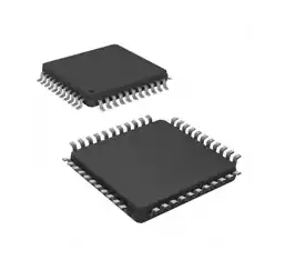


 工商网监
湘ICP备2023018690号
工商网监
湘ICP备2023018690号
