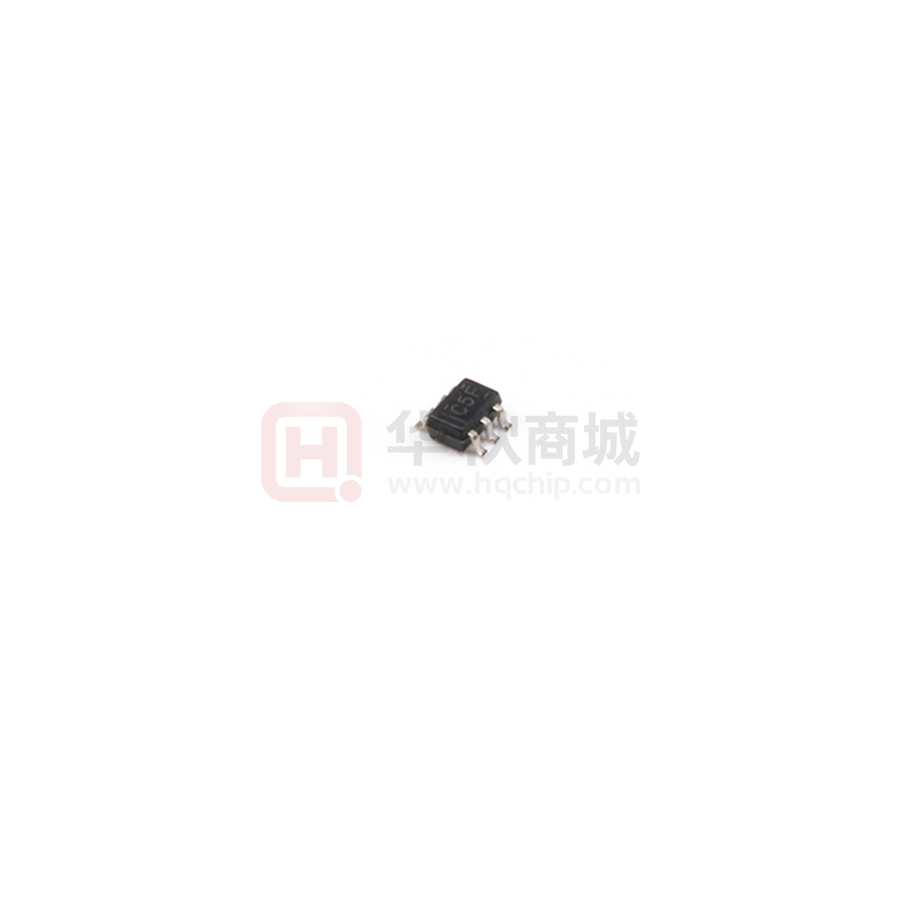
GS4157B
Low Voltage, SPDT 0.8Ω Analog Switch
Features
·
On-Resistance: 0.8Ω (TYP)
·
TTL/CMOS Compatible
·
-3dB Bandwidth: 80MHz
·
Operating Temperature: -40°C ~ +125°C
·
Single-Supply Operation: +1.8V ~ +5.5V
·
Small Package:
·
Break-Before-Make Switching
GS4157B Available in SOT23-6 and SC70-6 Packages
·
Rail-to-Rail Operation
·
Low Static Power
General Description
The GS4157B is low on-resistance (0.8Ω), fast single-pole double-throw (SPDT) CMOS switch with operation range +1.8V ~
+5.5V. The GS4157B is designed for low operating voltage, high current switching of signal gating, chopping, modulation or
demodulation (modem), and speaker output for cell phone applications.
The device contains a break-before-make (BBM) feature. The control input, IN, tolerates input drive signals up to 5.5V,
independent of supply voltage.
All devices are specified for the temperature range of -40℃ to +125℃.The GS4157B single is available in Green SC70-6 and
SOT23-6 packages.
Applications
·
Battery-Operated Equipment
·
Portable Systems
·
Wearable Devices
·
Cell Phones
·
Computer Peripherals
·
PDAs
Pin Configuration
Figure 1. Pin Assignment Diagram
August 2020-REV_V0
1/9
�GS4157B
Absolute Maximum Ratings
Condition
Min
Max
-0.5V
+7.5V
Analog Input Voltage (NC NO or COM)
Vss-0.5V
VDD+0.5V
PDB Input Voltage
Vss-0.5V
+7V
-40°C
+125°C
Power Supply Voltage (VDD to Vss)
Operating Temperature Range
Junction Temperature
+160°C
Storage Temperature Range
-55°C
Lead Temperature (soldering, 10sec)
+150°C
+260°C
Package Thermal Resistance (TA=+25℃)
SOT23-6, θJA
190°C/W
SC70-6, θJA
333°C/W
ESD Susceptibility
HBM
3500V
MM
300V
Note: Stress greater than those listed under Absolute Maximum Ratings may cause permanent damage to the device. This is a
stress rating only and functional operation of the device at these or any other conditions outside those indicated in the operational
sections of this specification are not implied. Exposure to absolute maximum rating conditions for extended periods may affect
reliability.
Package/Ordering Information
MODEL
CHANNEL
GS4157B
Single
PACKAGE
PACKAGE
MARKING
DESCRIPTION
OPTION
INFORMATION
GS4157B-CR
SC70-6
Tape and Reel,3000
4157B
GS4157B-TR
SOT23-6
Tape and Reel,3000
4157B
ORDER NUMBER
August 2020-REV_V0
2/9
�GS4157B
Electrical Characteristics
(At VS = +5V, and TA = +25℃, unless otherwise noted.)
PARAMETER
SYMBOL
CONDITIONS
TYP
MIN
MAX
UNITS
0
VS
V
ANALOG SWITCH
Analog Signal Range
VNO ,VNC ,VCOM
VS = 4.5V, VNO or VNC = 3.5V,
0.8
Ω
1.9
Ω
ICOM = -10mA, Test Circuit 1
On-Resistance
RON
VS = 2.7V, VNO or VNC = 1.5V,
ICOM = -10mA, Test Circuit 1
VS = 4.5V, VNO or VNC = 3.5V,
On-Resistance Match Between Channels
ΔRON
0.43
0.47
Ω
0.45
0.5
Ω
0.2
0.3
Ω
0.2
0.35
Ω
1
μA
1
μA
ICOM = -10mA, Test Circuit 1
VS = 2.7V, VNO or VNC = 1.5V,
ICOM = -10mA, Test Circuit 1
VS = 4.5V, VNO or VNC = 1.0V, 2.0V, 3.5V,
ICOM = -10mA, Test Circuit 1
On-Resistance Flatness
RFLAT(ON)
VS = 2.7V, VNO or VNC = 1.0V, 1.5V, 2.0V,
ICOM = -10mA, Test Circuit 1
Source OFF Leakage Current
INC(OFF) ,INO(OFF)
VS = 5.5V, VNO or VNC = 1.0V, 4.5V,
VCOM = 4.5V, 1.0V
Channel ON Leakage Current
INC(ON) ,INO(ON) ,ICOM(ON)
VS = 5.5V, VCOM = 1.0V, 4.5V
VNO or VNC = 1.0V, 4.5V, or floating
DIGITAL INPUTS
Input High Voltage
Input Low Voltage
Input Leakage Current
VS = 5V
1.5
V
VS = 3V
0.9
V
VINH
VS = 5V
0.55
V
VS = 3V
0.45
V
1
μA
VINL
IIN
VS = 5.5V, VIN = 0V or 5.5V
August 2020-REV_V0
3/9
�GS4157B
Electrical Characteristics
(At VS = +5V, and TA = +25℃, unless otherwise noted.)
PARAMETER
SYMBOL
CONDITIONS
TYP
MIN
MAX
UNITS
DYNAMIC CHARACTERISTICS
VS = 5V, VNO or VNC = 3V, VIN_H = 1.5V, VIN_L = 0V,
20
ns
28
ns
23
ns
22
ns
23
ns
27
ns
VS = 5V, RS = 39Ω, CL = 50pF, Test Circuit 4
9
ns
VS = 3V, RS = 39Ω, CL = 50pF, Test Circuit 4
9
ns
RL = 300Ω, CL = 35pF, Test Circuit 2
Turn-On Time
TON
VS = 3V, VNO or VNC = 1.5V, VIN_H = 1.5V, VIN_L = 0V,
RL = 300Ω, CL = 35pF, Test Circuit 2
VS = 5V, VNO or VNC = 3V, VIN_H = 1.5V, VIN_L = 0V,
RL = 300Ω, CL = 35pF, Test Circuit 2
Turn-Off Time
TOFF
VS = 3V, VNO or VNC = 1.5V, VIN_H = 1.5V, VIN_L = 0V,
RL = 300Ω, CL = 35pF, Test Circuit 2
VS = 5V, VNO1 or VNC1 = VNO2 or VNC2 = 3V,
RL = 300Ω, CL = 35pF, Test Circuit 3
Break-Before-Make Time Delay
TBBM
VS = 3V, VNO1 or VNC1 = VNO2 or VNC2 = 3V,
RL = 300Ω, CL = 35pF, Test Circuit 3
Skew
Off Isolation
-3dB Bandwidth
TSKEW
RL = 50Ω, Signal = 0dBm,
f=10MHz
-40
db
CL = 5pF, Test Circuit 5
f=1MHz
-60
db
RL = 50Ω, Signal = 0dBm, CL = 5pF, Test Circuit 6
80
MHz
OISO
BW
Source OFF Capacitance
CNC(OFF) ,CNO(OFF)
f=1MHz
20
pF
Channel ON Capacitance
CNC(ON) ,CNO(ON) ,CCOM(ON)
f=1MHz
73
pF
POWER REQUIREMENTS
Power Supply Range
VS
Power Supply Current
IS
1.8
VIN = 0V or VS
5.5
V
1
μA
August 2020-REV_V0
4/9
�GS4157B
Typical Performance characteristics
o
At TA=+25 C, and VS=+5V, unless otherwise noted.
BANDWIDTH
On Response(db)
On Response(db)
BANDWIDTH
Frequency(MHz) VS=+5V
Frequency(MHz) VS=+3V
RON(Ω)
Typical RON vs Input Voltage (VI
(VI)
VI(V)
August 2020-REV_V0
5/9
�GS4157B
Parameter Measurement Information
Test Circuit 1. On-Resistance
0.1μF
50%
50%
IN
VDD
90%
90%
Vout
COM
NC/NO
Vout
IN
VSS
CL
RL
300Ω 35pF
TON
TOFF
Test Circuit 2. Switching Times
0.1μF
IN
50%
VDD
COM
NC
NO
IN
90%
90%
Vout
Vout
VSS
CL
RL
300Ω 35pF
TBBM
Test Circuit 3. Break-Before-Make Time Delay
August 2020-REV_V0
6/9
�GS4157B
Parameter Measurement Information
Test Circuit 4. Output Signal Skew
Test Circuit 5. Off Isolation
Test Circuit 6. -3dB Bandwidth
August 2020-REV_V0
7/9
�GS4157B
Package Information
SC70-6
August 2020-REV_V0
8/9
�GS4157B
SOT23-6
August 2020-REV_V0
9/9
�
