Designated client product
This product will be discontinued its production in the near term.
And it is provided for customers currently in use only, with a time limit.
It can not be available for your new project. Please select other new or
existing products.
For more information, please contact our sales office in your region.
New Japan Radio Co.,Ltd.
www.njr.com
�NJM2903/2403
SINGLE-SUPPLY DUAL COMPARATOR
■ GENERAL DESCRIPTION
The NJM2903/2403 consist of two independent precision voltage
comparators with an offset voltage specification as low as 5.0mV max
for two comparators, which were designed specifically to operate from a
single power supply over a wide range of voltages. Operation from split
power supplies is also possible and the low power supply current drain is
independent of the magnitude of the power supply voltage. The
NJM2903/2403 have unique characteristic: the input common-mode
voltage range includes ground, even though operated from a single
power supply voltage. Application areas include limit comparators,
simple analog-to-digital converters; pulse, square-wave and time delay
generators; wide range VCO; MOS clock timers; multivibrators and high
voltage digital logic gates. The NJM2903/2403 were designed to directly
interface with TTL and MOS. When operated from both plus and minus
power supplies, the NJM2903/2403 will directly interface with MOS logic
where their low power drain is a distinct advantage over standard
comparators.
■ FEATURES
● Operating Voltage
● Single Supply Operation
● Open Collector Output
● High Output Sink Current
● Package Outline
■ PACKAGE OUTLINE
NJM2903D/2403D
( DIP8 )
NJM2903M/2403M
( DMP8 )
NJM2903V/2403V
( SSOP8 )
NJM2903L/2403L
( SIP8 )
NJM2903RB1
( MSOP8 (TVSP8))
NJM2903E
( SOP8 )
+2V~+36V
15mA (@ NJM2403)
DIP8, DMP8, SIP8, SSOP8,
NJM2903 only: SOP8 JEDEC 150mil,
:MSOP8 (TVSP8) MEET JEDEC MO-187-DA / THIN TYPE
● Bipolar Technology
■ PIN CONFIGURATION
( Top View )
1
8
A
2
3
4
A
B
7
B
6
5
NJM2903D/2403D, NJM2903M/2403M
NJM2903V/2403V, NJM2903E/2903RB1
1
2
3
4
5
6
7
NJM2903L/2403L
8
PIN FUNCTION
1. A OUTPUT
2. A - INPUT
3. A +INPUT
4. GND
5. B +INPUT
6. B - INPUT
7. B OUTPUT
8. V+
■ EQUIVALENT CIRCUIT ( 1/2 Shown )
V+
+ INPUT
- INPUT
OUTPUT
GND
Ver.2012-09-14
-1-
�NJM2903/2403
■ ABSOLUTE MAXIMUM RATINGS
( Ta=25˚C )
PARAMETER
Supply Voltage
Differential Input Voltage
Input Voltage
SYMBOL
V+
VID
VIN
Power Dissipation
PD
Operating Temperature Range
Storage Temperature Range
Topr
Tstg
RATINGS
36 ( or ±18 )
36
-0.3~+36
( DIP8 ) 500
( DMP8 ) 300
( SSOP8 ) 250
( SIP8 ) 800
(SOP8) 300
(MSOP8(TVSP8))320
-40~+85
-50~+125
UNIT
V
V
V
mW
˚C
˚C
■ ELECTRICAL CHARACTERISTICS
( V+=5V,Ta=25˚C )
PARAMETER
SYMBOL
Input Offset Voltage
Input Offset Current
Input Bias Current
Input Common Mode Voltage Range
Large Signal Voltage Gain
Response Time
Output Sink Current
Output Saturation Voltage
Output Saturation Voltage
Output Leakage Current
Operating Current
VIO
IIO
IB
VICM
AV
tR
ISINK
VSAT
VSAT
ILEAK
ICC
-2-
TEST CONDITION
RS=0Ω,VO=1.4V
RL=15kΩ
RL=5.1kΩ
VIN-=1V,VIN+=0V,VO=1.5V
VIN-=1V,VIN+=0V,ISINK=3mA
VIN-=1V,VIN+=0V,ISINK=15mA
VIN-=0V,VIN+=1V,VO=5V
2903
2403
MIN.
TYP.
MAX.
MIN.
TYP.
MAX.
0~3.5
6
-
30
106
1.5
200
0.4
7
50
250
400
1.0
1.0
0~3.5
20
-
40
106
1.5
200
0.5
10
100
500
400
1.0
1.5
UNIT
mV
nA
nA
V
dB
µs
mA
mV
mV
µA
mA
Ver.2012-09-14
�NJM2903/2403
■ TYPICAL CHARACTERISTICS
Ver.2012-09-14
-3-
�NJM2903/2403
■ TYPICAL CHARACTERISTICS
■ TYPICAL APPLICATIONS
Comparator With Hysteresis
Pulse Generator
Output Strobing Circuit
OUTPUT
Strobe Input
[CAUTION]
The specifications on this databook are only
given for information , without any guarantee
as regards either mistakes or omissions. The
application circuits in this databook are
described only to show representative usages
of the product and not intended for the
guarantee or permission of any right including
the industrial rights.
-4-
Ver.2012-09-14
�
很抱歉,暂时无法提供与“NJM2403M”相匹配的价格&库存,您可以联系我们找货
免费人工找货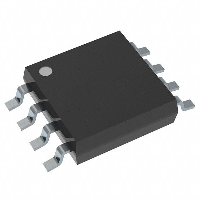


 工商网监
湘ICP备2023018690号
工商网监
湘ICP备2023018690号
