Designated client product
This product will be discontinued its production in the near term.
And it is provided for customers currently in use only, with a time limit.
It can not be available for your new project. Please select other new or
existing products.
For more information, please contact our sales office in your region.
New Japan Radio Co.,Ltd.
www.njr.com
�NJM5534
HIGH PERFORMANCE LOW-NOISE OPERATIONAL AMPLIFIER
■ GENERAL DESCRIPTION
The NJM5534 is a high performance low noise operational amplifier.
This amplifier features popular pin-out, superior noise performance,
and high output drive capability. And also, features guaranteed noise
performance with substantially higher gain-bandwidth product, power
bandwidth, and slew rate which far exceeds that of the NJM741 type
amplifiers.
The specially designed low noise input transistors allow the
NJM5534 to be used in very low noise signal processing applications
such as audio pre-amplifiers and servo error amplifiers.
The NJM5534 is internally compensated for a gain of three or higher.
Externally compensation for optimizing specific performance can be
obtained by use of an external compensation capacitor between
COMPENSATION(5PIN) and BALANCE/COMPENSATION(8PIN).
If very low noise characteristic is of prime importance, it is
recommended D-Rank type products(NJM5534DD/MD). These
have specified maximum limits for equivalent input noise voltage.
■ FEATURES
● Operating Voltage
● Single Circuit
● With BALANCE Terminal
● Low Input Noise Voltage
● Power Bandwidth
● Slew Rate
● Package Outline
● Bipolar Technology
■ PACKAGE OUTLINE
NJM5534D
(DIP8)
NJM5534M
(DMP8)
±3V~±22V
3.3nV/√Hz typ.@1kHz
200kHz typ.
13V/µs typ.
DIP8, DMP8
■ PIN CONFIGURATION
(Top view)
1
8
2
7
3
6
4
5
DIP8, DMP8 Package
PIN FUNCTION
1.BALANCE
2.–INPUT
3.+INPUT
4.V5.COMPENSATION
6.OUTPUT
7.V+
8.BALANCE/COMPENSATION
■ EQUIVALENT CIRCUIT
Ver.2011-02-22
-1-
�NJM5534
■ ABSOLUTE MAXIMUM RATINGS (Ta=25˚C)
PARAMETER
Supply Voltage
SYMBOL
+
RATING
-
UNIT
V /V
±22
V
Differential Input Voltage
VID
±0.5
V
Common Mode Input Voltage
VIC
V
Power Dissipation
PD
mW
Operating Temperature Range
Topr
V+/VDIP8: 500
DMP8: 300
-20~+75
Storage Temperature Range
Tstg
-40~+125
°C
RATING
UNIT
±3~±22
V
°C
■ RECOMMENDED OPERATING VOLTAGE (Ta=25˚C)
PARAMETER
Supply Voltage
SYMBOL
+
-
V /V
■ ELECTRICAL CHARACTERISTICS (Ta=25˚C,V+/V-=±15V, unless otherwise noted.)
PARAMETER
SYMBOL
TEST CONDITION
RS≤10kΩ
MIN.
TYP.
MAX.
UNIT
-
0.5
4
mV
Input Offset Voltage
VIO
Input Offset Current
IIO
-
20
300
nA
Input Bias Current
IB
-
500
1500
nA
Input Resistance
RIN
30
100
-
kΩ
Large Signal Voltage Gain
AV
RL≥2kΩ, VO=±10V
88
100
-
dB
Maximum Output Voltage
VOM
RL≥600Ω
±12
±13
-
V
Common Mode Input Voltage Range
VICM
±12
±13
-
V
Common Mode Rejection Ratio
CMR
RS≤10kΩ
70
100
-
dB
Supply Voltage Rejection Ratio
SVR
RS≤10kΩ
80
100
-
dB
Supply Current
ICC
RL=∞
-
4
8
mA
Trainsient Response Rise Time
tR
VIN=50mV, RL=600Ω, CL=100pF, Cc=22pF
-
35
-
ns
VIN=50mV, RL=600Ω, CL=100pF, Cc=22pF
-
17
-
%
Cc=0
-
13
-
V/µs
Overshoot
Slew Rate
SR
Gain Bandwidth Product
GB
Cc=22pF, CL=100pF
-
10
-
MHz
Power Bandwidth
WPG
Vo=20VPP, Cc=0
-
200
-
kHz
Equivalent Input Noise Voltage
VNI
f=20Hz~20kHz
-
1
-
µVrms
Equivalent Input Noise Current
INI
f=20Hz~20kHz
-
25
-
pArms
Equivalent Input Noise Voltage
en
Equivalent Input Noise Current
in
Broadband Noise Figure
NF
fO=30Hz
-
5.5
-
nV/√Hz
fO=1kHz
-
3.3
-
nV/√Hz
fO=30Hz
-
1.5
-
pA/√Hz
fO=1kHz
-
0.4
-
pA/√Hz
f=10Hz~20kHz, RS=5kΩ
-
0.9
-
dB
■ ELECTRICAL CHARACTERISTICS (D-rank type(Note1), V+/V-=±15V, Ta=25°C, unless otherwise noted.)
PARAMETER
Equivalent Input Noise Voltage
SYMBOL
VNI
TEST CONDITION
RIAA, RS=2.2kΩ
MIN.
TYP.
MAX.
UNIT
-
-
1.4
µVrms
(Note1)D-rank type is a Equivalent Input Noise Voltage selected product.
-2-
Ver.2011-02-22
�NJM5534
■ TYPICAL CHARACTERISTICS
Gain/Phase vs. Frequency
50
20
20
-40
10
-80
0
-120
-10
-160
-20
10k
100k
1M
10M
Frequency [Hz]
Phase [deg]
0
Maximum Output Voltage [V]
Phase
30
10
-Vom
V+/V-=±15V
5
0
-5
-10
-15
V+/V-=±22V
-25
10
100
1k
Load Resistance [Ω]
20
15
10
5
V+/V-=±15V, Ta=25ºC
30
Cc=0pF
25
Cc=50pF
Cc=20pF
20
15
10
5
0
10k
10M
100k
Frequency [Hz]
Voltage Noise vs. Source Resistance
THD vs. Output Voltage
V+/V-=±15V, Ta=25ºC
V+/V-=±15V, RL=10kΩ, Gv=20dB, Ta=25ºC
100
10k
Maximum Output Voltage Swing vs. Frequency
Maximum Output Voltage Swing
[Vpp]
25
100k
1M
Frequency [Hz]
V+/V-=±15V
35
30
0
10k
+Vom
-20
-200
100M
V+/V-=±15V, Ta=25ºC
35
V+/V-=±22V
15
Maximum Output Voltage Swing vs. Frequency
Maximum Output Voltage Swing
[Vpp]
Ta=25ºC
25
Gain
40
Voltage Gain [dB]
Maximum Output Voltage vs. Load Resistance
Ta=25ºC
0.01
1M
Total Harmonic Distortion [%]
Equivalent Input Noise Voltage
[µVrms]
Weighting
100 10k
Rs
10
Flat
100kHz LPF
1
JIS A
0.1
f=20kHz
0.001
f=20Hz
f=1kHz
0.0001
10
Ver.2011-02-22
100
1k
Source Resistance [Ω]
10k
1
10
Output Voltage [Vrms]
-3-
�NJM5534
■ TYPICAL CHARACTERISTICS
Supply Current vs. Temperature
Input Offset Voltage vs. Temperature
9
2.5
8
2
Input Offset Voltage [mV]
Supply Current [mV]
V+/V-=±15V
7
6
5
4
3
2
1.5
1
0.5
0
-0.5
-1
1
0
-1.5
-50
-25
0
25
50
75
100
Ambient Temperature [ºC]
125
-50
V+/V-=±15V
900
-25
0
25
50
75
100
Ambient Temperature [ºC]
125
Maximum Output Voltage vs. Temperature
Input Bias Current vs. Temperature
V+/V-=±15V, RL=600Ω
15
Maximum Output Voltage [V]
800
Input Bias Current [nA]
V+/V-=±15V
700
600
500
400
300
200
100
0
+Vom
10
5
0
-5
-10
-Vom
-15
-50
-25
0
25
50
75
100
Ambient Temperature [ºC]
125
-50
-25
0
25
50
75
100
Ambient Temperature [ºC]
125
Slew Rate vs. Compensation Capacitance
Ta=25ºC
16
14
Slew Rate [V/µs]
12
10
8
6
4
2
0
0
-4-
10 20 30 40 50 60 70 80 90 100
Compensation Capacitance Cc [pF]
Ver.2011-02-22
�NJM5534
■ TEST CIRCUIT
+15V
Noise Voltage (RIAA) measurement circuit
100µ
Rs
2.2k
3.3µ
-15V
100µ
40dB Amp
30kHz LPF
0.47µ
2.2µ
Vout
56k
30k
330k
0.0024µ
0.0082µ
220k
47µ
610
■ ADJUSTMENT METHOD
Fig.1-1, Fig.1-2 shows the input offset voltage adjustment circuit, and frequency compensation circuit.
Without these features, the adjustment pins are open.
Fig.1-1 Input Offset Voltage Adjustment
Fig.1-2 Frequency Compensation
+
V
22k
Cc
100k
2
1
8
2
6
8
5
6
3
3
■ NOTICE
When used in voltage follower circuit, put a current limit resistor into non-inverting input terminal in order to avoid inside
input diode destruction when the power supply is turned on. ( ref.Fig.2 )
1k
OUTPUT
INPUT
Fig.2
[CAUTION]
The specifications on this databook are only
given for information , without any guarantee
as regards either mistakes or omissions. The
application circuits in this databook are
described only to show representative usages
of the product and not intended for the
guarantee or permission of any right including
the industrial rights.
Ver.2011-02-22
-5-
�
很抱歉,暂时无法提供与“NJM5534M-TE2”相匹配的价格&库存,您可以联系我们找货
免费人工找货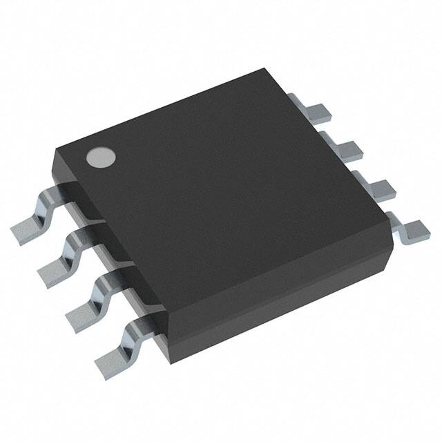


 工商网监
湘ICP备2023018690号
工商网监
湘ICP备2023018690号
