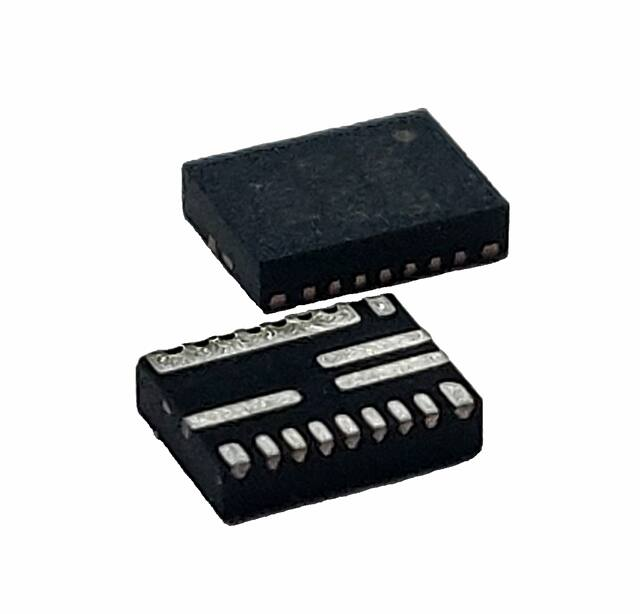
IS6607A
3.5V to 16V Input, 20A Sync Step-Down Converter W/ Light Load
Mode, Programmable Switching Frequency and Over Current Limit
Rev2.6 05/2020
Part Number
IS6607A
Input Voltage
3.5V~16V
Output Voltage
0.6V~5.5V
Current Rating
20A
Description
The IS6607A is a high power density, fully
integrated synchronous buck converter. It
works with wide input voltage range and can
support up to 20A continuous output current at
defined conditions. LDO is integrated
internally, which is very suitable for single
input supply condition. External bias is
optional for maximizing the efficiency. A
differential sensing scheme and a 0.6V
internal feedback reference voltage achieve
±1% output voltage tolerance over full
temperature range. The IS6607A provides
excellent line and load regulation.
Switching
frequency
can
be
easily
programmed among 600kHz, 800kHz and
1MHz. The IS6607A uses patented Turbo
Constant On Time (TCOTTM) to control the
algorithm with fast transient response. Pure
MLCC output capacitors can be used to save
space and cost.
The IS6607A has fully integrated protection
features including OCP, NOCP, OVP, UVP
and over temperature protection (OTP).
Features
Turbo Constant On Time (TCOTTM) Control
with Fast Transient Response.
• VIN Input Voltage Range: 2.4 V to 16V with
External Bias VCC voltage, or 3.5V to 16V
with Internal Bias VCC.
• Output Voltage Range: 0.6V to 5.5V, and
90% Max Duty Cycle.
• 20A Continuous Output Current.
•
Excellent Load and Line Regulations with
1% Voltage Accuracy.
• Up to 90% Efficiency at VIN=12V,
VOUT=1.2V
•
Differential Remote Sense
• Mode Selection between Pulse Skip and
CCM at Light Load
•
Output Voltage Track and Discharge
• Pre-bias Start-up
•
•
The IS6607A is available in a QFN 3mm x
4mm package with 21-Pin.
Junction Temperature Range from -40ºC
to 125ºC
•
Programmable Soft-Start Time
Moisture Sensitivity Leve 3.
•
1.0µA Current into VIN Pin during
Shutdown
Programmable Valley Current Limit
Programmable Switching Frequency:
600kHz, 800kHz and 1MHz
OCP, NOCP, OVP, UVLO and OTP
QFN 3mm x 4mm Package with 21-Pin
Applications
•
•
•
Computers and Servers POLs
Telecom/Datacom POLs
Point of Load Module
Production Datasheet
•
•
•
•
Innovision Semiconductor
1
�IS6607A
Rev2.6 05/2020
Typical Application Circuit
C4
R6
BST
L1
VIN
VIN
C1
PHASE
VO
C2
VCC
C8
FB
C3
R1
C9
R4
PGOOD
PGD
IS6607A
ON
R5
RTN
EN
OFF
C6
MODE
R3
Production Datasheet
PG ND
CS
R2
AG ND
REF
Innovision Semiconductor
2
�IS6607A
Rev2.6 05/2020
Order Information
Part Number
Package
Shipping Method
Package Marking
IS6607A
QFN-21(3mm x 4mm)
5000u Tape & Reel
IS6607A
TOP MARKING (IS6607A)
IS6607A
C12TC8
YYWW
IS: Innovision Semiconductor prefix
6607A: First five digits of the part number
C12TC8: Production site
Y: Year code
W: Week code
Package Reference
VIN
21
PHASE
20
BST 1
19
VCC
AGND 2
18
PGND
CS 3
17
PGND
MODE 4
16
PGND
REF 5
15
PGND
RTN 6
14
PGND
FB 7
13
PGND
EN 8
12
PGND
11
PGND
PGOOD 9
10
VIN
Top View
Production Datasheet
Innovision Semiconductor
3
�IS6607A
Rev2.6 05/2020
Absolute Maximum Ratings
Thermal Ratings
Supply Voltage (Vin) …………………. -0.3V to 20V
Vcc Voltage (Vcc)…………………………-0.3V to 5.5V
Switch Node Voltage (VPH) DC…………-0.3V to 20V
Switch Node Voltage (VPH) 25ns……...-5V to 25V
BST Pin (Vbst-sw) DC………………… -0.3V to 5.5V
All other pins……………………………-0.3V to 5.5V
Junction Temperature (T j )………………….150°C
Storage Temperature…………………-65°C to 150°C
Θ JC Max…………………………………….17°C/W
ΘJB Typ (Still Air, No Heat sink) …………….8°C/W
Recommended Operating Conditions
Supply Voltage (Vin)………………………2.4V to 16V
V c c Voltage (V cc )…………………….3.0V to 5V
Output Voltage (Vo)………………………0.6V to 5.5V
Max Output Current (I o_max)…………………… 20A
Junction Temperature (T j)……….. -40°C to 125°C
Note 1. Stresses beyond those listed under “Absolute Maximum Ratings” may cause permanent damage to the device. These are stress
ratings only; functional operation of the device at these or any other conditions beyond those indicated in the operational sections of the
specifications is not implied. Exposure to absolute maximum rating conditions for extended periods may affect device reliability.
ESD Ratings
Electrostatic Discharge
Standard
Value
Human Body Mode (HBM)
Charge Device Mode (CDM)
JEDEC EIA/JESD22-A114
JEDEC EIA/JESD22-C101F
±1500V
±2000V
1). JEDEC document JEP155 states that 500-V HBM allows safe manufacturing with a standard ESD control process.
2). JEDEC document JEP157 states that 250-V CDM allows safe manufacturing with a standard ESD control process.
Production Datasheet
Innovision Semiconductor
4
�IS6607A
Rev2.6 05/2020
Pin Out and Package
IS6607A(QFN-21)
Pin Number
Name
Description
Bootstrap connection. Connect a capacitor between PHASE and BST, which
is required to form a floating supply across the high-side switch driver.
1
BST
2
AGND
3
CS
4
MODE
5
REF
Connect a capacitor to PGND to set soft start time or to an external reference
for output voltage tracking. The capacitance of this capacitor determines the
soft-start time.
6
RTN
Output remote sense feedback. Connect the pin to the negative side of the
voltage sense point.
7
FB
Output remote sense return. An external resistor divider from the output to RTN
(tapped to FB) sets the output voltage.
8
EN
Enable pin. An input signal turns the regulator on or off. Connect EN to VIN
through a pull-up resistor. Do not float this pin.
9
PGOOD
Power good output with open drain. If the output voltage is within regulation,
the pull-up resistor is required to indicate high.
10, 21
VIN
Supply voltage. Input to the power stage and internal LDO. Make the
connection with wide PCB traces.
11~18
PGND
System ground. PGND is power ground of the power stage. Make the
connection with wide PCB traces.
19
VCC
Internal 5V LDO output. Supply power for the drive and control circuits.
20
PHASE
Production Datasheet
Signal logic ground. A Kelvin connection to PGND is required.
Current limit and inductor current report. Connect a resistor to AGND to set the
valley current limit trip point. A voltage indicating the inductor current during
operating.
Operation mode selection. Connect a resistor to AGND to set switching
frequency and DCM/FCCM operation.
Switch output. Switch node of power stage. Connect PH to the inductor and
bootstrap capacitor. Make the connection with wide PCB traces.
Innovision Semiconductor
5
�IS6607A
Rev2.6 05/2020
FUNCTIONAL BLOCK DIAGRAM
VIN
MODE
VCC
MODE
Select
LDO
BST
REG
BST
Off
Timer
EN
Reference
System
Monitor
HS
Driver
xS
OV_TH UV_TH
REF
RTN
+
-Error
Amplifier
FB
Q
+
PWM
Comparator
PHASE
Logic
Control
On
Timer
Ramp
HSG
OV_TH
+
PGOOD
PGOOD
Comparator
UV_TH
LSG
LS
Driver
+
-
HSG
LSG
xR
OV Detect
Comparator
+
ZCD
UV Detect
Comparator
xLIM
Valley
Current
Limit&
ZCD
PGND
FAULT
CS
Production Datasheet
Innovision Semiconductor
6
�IS6607A
Rev2.6 05/2020
ELECTRICAL CHARACTERISTICS
Definition/Datasheet
Parameters
Min
Typ
Unit
Max
SUPPLY VOLTAGE & CURRENT
VIN Supply Voltage (with internal LDO)
3.5
16
V
VIN Supply Voltage (with external bias VCC voltage)
2.4
16
V
VIN Supply Current (Quiescent)
EN=2V ,VFB = 1V
VIN Shutdown Current
EN="Lo"
1950
0
µA
10
µA
VCC Supply
VCC Output Voltage (5.3V
2
×
8
×
where
•
•
COUT(min) is the minimum output
capacitance needed to meet the stability
requirement of the design
tON is the on-time information based on the
switching frequency and duty cycle (in this
design, 100 ns)
•
τ is the ramp compensation time
constant of the design based on the
switching frequency and duty cycle (in
this design, 1 sec)
•
LOUT is the output inductance (in the
design, 0.39 µH)
Production Datasheet
Use the next equation to estimate the amount
of capacitance needed for a given dynamic
load release.
_
=
×∆
2×∆
_
×
In general applications where the overall output
voltage tolerance is +/-5%, the allowed
transient voltage deviation during the worst
case load release can be set at around 3%
depending on how much output voltage
setpoint accuracy (1% in this design) and the
ripple voltage requirement (1% in this design).
The minimum output capacitance to meet the
overshoot requirement can be calculated using
the above equation. This example uses a
combination of POSCAP and MLCC capacitors
to meet the overshoot requirement.
•
POSCAP bank #1: 2 x 470 µF, 2.5 V, 6 mΩ
per capacitor
Innovision Semiconductor
17
�IS6607A
Rev2.6 05/2020
•
MLCC bank #2: 4 × 100 µF, 2.5 V, 1 mΩ per
capacitor with DC+AC derating factor of
50%
Recalculating the worst case overshoot using
the described capacitor bank design, the
overshoot needs to be 30 mV or less which
meets the 3% overshoot transient specification
requirement.
Output Voltage Ripple
The output voltage ripple is another important
design consideration. The following equation
calculates the minimum output capacitance
required to meet the output voltage ripple
specification. This criterion is the requirement
when the impedance of the output capacitance
is dominated by ESR.
_
=
8×
×
_
In this example, the maximum output voltage
ripple is 5.5 mV. Because this capacitance
value is significantly lower compared to that of
transient load release, determining the output
capacitance bank using the worst case load
release requirement is generally adequate.
Because the output capacitor bank consists of
both POSCAP and MLCC type capacitors, it is
important to consider the ripple effect at the
switching frequency due to effective ESR.
For detailed calculations, please contact the
factory to obtain a user-friendly Excel based
design tool.
4.
Input Capacitor Selection
The IS6607A devices require a high-quality,
ceramic, type X5R or X7R, input decoupling
capacitor with a value of at least 1 μF of
effective capacitance on the VCC pin, relative
to AGND. The power stage input decoupling
capacitance (effective capacitance at the VIN
and PGND pins) must be sufficient to supply
the high switching currents demanded when
the high-side MOSFET switches on, while
providing minimal input voltage ripple as a
result. This effective capacitance includes any
DC bias effects. The voltage rating of the input
capacitor must be greater than the maximum
input voltage. The capacitor must also have a
ripple current rating greater than the maximum
input current ripple to the device during full
load. The input ripple current can be calculated
using the equation below.
Production Datasheet
The value of a ceramic capacitor varies
significantly over temperature and the amount
of DC bias applied to the capacitor. The
capacitance variations due to temperature can
be minimized by selecting a dielectric material
that is stable over temperature. X5R and X7R
ceramic dielectrics are usually selected for
power regulator capacitors because they have
a high capacitance to volume ratio and are
fairly stable over temperature. The input
capacitor must also be selected with the DC
bias taken into consideration. For this design
example, a ceramic capacitor with at least a 25
V voltage rating is required to support the
maximum input voltage. For this design, allow
0.1 V input ripple for VRIPPLE(cap), and 0.3 V input
ripple for VRIPPLE(esr). the minimum input
capacitance for this design is 38.5 µF, and the
maximum ESR is 9.4 mΩ. For this example,
four 22 μF, 25 V low-ESR polymer capacitors in
parallel were selected for the power stage.
Bootstrap Capacitor Selection
A ceramic capacitor with a value of 0.1 μF must
be connected between the BOOT and SW pins
for proper operation. It is recommended to use
a ceramic capacitor with X5R or better grade
dielectric. Use a capacitor with a voltage rating
of 25 V or higher.
5.
R-C Snubber and VIN Pin HighFrequency Bypass
Though it is possible to operate the IS6607A
within absolute maximum ratings without
ringing reduction techniques, some designs
may require external components to further
reduce ringing levels. This example uses two
approaches: a high frequency power stage
bypass capacitor on the VIN pins, and an R-C
snubber between the PHASE area and GND.
The high-frequency VIN bypass capacitor is a
lossless ringing reduction technique which
helps minimizes the outboard parasitic
inductances in the power stage, which store
energy during the low-side MOSFET on-time,
and discharge once the high-side MOSFET is
turned on. For this design twin 2.2 nF, 25 V,
0603 sized high-frequency capacitors are used.
The placement of these capacitors is critical to
its effectiveness. Its ideal placement is shown
in PCB layout guidelines.
Innovision Semiconductor
18
�IS6607A
Rev2.6 05/2020
PCB Layout Guidelines
Efficient PCB layout is crucial to the stable
operation of the circuit. For best
performance, refer to the figure in the PCB
layout column and follow the PCB layout
recommendations below.
1.The input MLCC capacitor shall be as close
as possible to the VIN and PGND pins and
the main MLCC capacitor shall be placed on
the same wiring layer as IS6607A. The
copper plane of VIN and PGND can be
maximized to minimize the parasitic
impedance.
2. A capacitor with a minimum capacitance of
0.1μF must be close to pin 10(VIN pin). At
least two 20/10 mil vias are required to
connect the grounding end of the capacitor to
the ground plane of the PCB board.
Production Datasheet
3. Place as many PGND holes as possible
nearest to the PGND pin to minimize
parasitic impedance and thermal resistance.
4. VCC capacitor should be placed as close to
the IS6607A as possible. Connect AGND and
PGND at VCC capacitor's grounding point.
5. Place the BST capacitor
as close as
possible to BST and PH. Routing widths
should be greater than 20mil. It is
recommended to use a 0.1µF to 1µF
bootstrap capacitor. Place the BST
resistance between the IC and the BST
capacitor to achieve Damping effect. It is
recommended to use a 3.3Ω resistance.
6. Place the REF capacitor close to REF and
connected to the RTN. It is recommended to
use a 22nF capacitor.
Innovision Semiconductor
19
�IS6607A
Rev2.6 05/2020
Typical Application Circuits
VIN
C4
0.1uF
C5
PHASE
R1
1
1.0V @ 20A
12
9
EN
8
PGND
MODE
4
CS
3
BST
C7
VCC
U1
PGOOD
EN
FB
R3
3k
MODE
R6
4k
FB
RTN
6
RTN
CS
R2
2k
NC
7
IS6607A
2
R5
0
VOUT
13
PHASE
PGND
R4
10k
VIN
5
REF
C11
0.22uF
C12
NC
REF
11
PGOOD
10,14
C6
1uF
L1
390nH
AGND
VCC
PGND
PGND
AGND
AGND
AGND
PGND
BST
VIN
C4
0.1uF
C5
PHASE
1
R1
12
9
EN
8
PGND
MODE
4
CS
3
R6
4k
PHASE
VOUT
13
C7
VCC
U1
PGOOD
EN
FB
MODE
CS
NC
7
R2
8.2k
R3
1.1k
IS6607A
RTN
2
R5
0
VIN
PGND
R4
10k
C6
1uF
5V @ 10A
L1
3.3uH
BST
10,14
REF
FB
RTN
6
5
C11
0.22uF
C12
NC
REF
11
PGOOD
PGND
AGND
VCC
PGND
AGND
AGND
AGND
Production Datasheet
PGND
Innovision Semiconductor
20
�IS6607A
Rev2.6 05/2020
PCB layout
TOP Layer
Layer 2
Production Datasheet
Innovision Semiconductor
21
�IS6607A
Rev2.6 05/2020
Layer 3
Bottom Layer
Production Datasheet
Innovision Semiconductor
22
�IS6607A
Rev2.6 05/2020
Package Dimension
Production Datasheet
Innovision Semiconductor
23
�IS6607A
Rev2.6 05/2020
RECOMMENDED LAND PATTERN
2.80
0.30
0.15×45
2.30
0.90
0.80
0.30
0.50
0.30
0.00
0.20
0.30
0.40
0.40
0.20
0.50
0.35
2.30
0.80
0.30
0.80
0.60
Production Datasheet
Innovision Semiconductor
24
�IS6607A
Rev2.6 05/2020
Reflow Specification
Qualification Reflow: The IS6606 was qualified in accordance with IPC/JEDEC J-STD-020D.01.
This standard classifies proper packaging, storage and handling in order to avoid subsequent
thermal and mechanical damage during the solder reflow attachment phase of PCB assembly.
The qualification preconditioning process specifies a sequence consisting of a bake cycle, moisture
soak cycle (in a temperature humidity oven), and three consecutive solder reflow cycles, followed by
functional device testing.
SUPPLIER TP≥TC
USER TP≤TC
TC
TC -5℃
SUPPLIER tp
USER tp
TP
tp
MAXIMUM RAMP UP RATE = 3℃/s
MAXIMUM RAMP DOWM RATE = 6℃/s
TL
TSMAX
PREHEAT AREA
TC -5℃
tL
TMEPERATURE[℃]
TSMIN
ts
25
TIME 25℃ TO PEAK
TIME
Production Reflow:
PROFILE FEATURE
SN - PB EUTECTIC ASSEMBLY
PB-FREE ASSEMBLY
Peak package body
temperature (TP)
For users, TP must not exceed
For users, TP must not exceed
TC(235℃).For suppliers, TP must TC(260℃).For suppliers, TP must
equal or exceed TC(235℃).
equal or exceed TC(260℃).
Storage Specifications
The storage specification of the IS6606 conforms to IPC/JEDEC J-STD-020D.01 Moisture
Sensitivity Level (MSL) 3.
After opening moisture-sealed bag
Production Datasheet
168 hours -- Storage conditions: ambient ≤30°C at 60%RH
Innovision Semiconductor
25
�IS6607A
Rev2.6 05/2020
TAPE AND REEL INFORMATION
REEL DIMENSIONS
TAPE DIMENSIONS
E
Discharging direction
P1
P0
D0
P2
B0
T
Reel Diameter
K0
1
.
.
.
.
.
W
F
Pin1
Discharging
direction
A0
Reel Width
NOTE:
KEY PARAMETER LIST OF TAPE AND REEL
Reel
Diameter
(inch)
Package Type
QFN-21(3 x 4)
1). The cumulative error of any 10 ratchet holes shall not exceed
±0.2mm
2). The non-parallelism of 100mm long carrier band in the carrier band
length direction shall not exceed 1mm.
Reel Width
(mm)
3). All dimensions are in accordance with EIA-481-3
4). Material: black, PS material, thickness 0.3±0.05mm.
5). The picture is only for reference. Please make the object as the
standard.
13″
Unit(mm)
ITEM
W
A0
B0
K0
P0
P1
P2
F
S
E
D0
T
DIM
12
±0.30
3.20
±0.1
4.20
±0.1
0.85
4.00
±0.1
8.00
±0.1
2.00
±0.1
5.5
±0.1
0.0
±0.1
1.75
±0.1
1.5
0.3
±0.05
Production Datasheet
+0.1
-0.05
Innovision Semiconductor
+0.10
-0.00
26
�


 工商网监
湘ICP备2023018690号
工商网监
湘ICP备2023018690号
