XL-5050RGBC-WS2812B
Technical Data Sheet
haracteristic
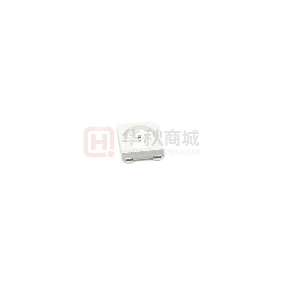
* 外观尺寸(L/W/H):5.0*5.0*1.6mm
Outline Dimensions (L / w / h): 5.0 * 5.0* 1.6 mm
* 发光颜色及胶体: 高亮度RGB/透明胶体
Luminous color and colloid: high brightness RGB / transparent colloid
* 环保工艺符合ROHS标准
Environmental protection products Complied With RoHS Directive
* EIA规范标准包装
EIA standard packaging
* 适用于SMT贴片自动化生产
Suitable for SMT automatic production
* 适用于回流焊制程
Suitable for reflow soldering process
product application
* LED全彩发光字灯串,LED全彩模组
LED full-color luminous character string, LED full-color module
* LED全彩软灯条硬灯条
LED full-color soft light strip hard light strip
* 电器设备跑马灯
Electric equipment marquee
* 智能音箱,风扇
Smart speaker, fan
* 显示屏,像素屏,点光源,LED异形屏
Display screen, pixel screen, point light source, LED special-shaped screen
* 各种电子产品
Various electronic products
1
�Catalogue
Electrical Characteristics.............................................................................................................................3
Typical Characteristic Curves......................................................................................................................6
Reliability Test Items And Conditions......................................................................................................10
Outline Dimensions.......................................................................................................................................11
Packaging......................................................................................................................................................12
Guideline for Soldering.............................................................................................................................. 14
Precautions....................................................................................................................................................16
2
�产品概述:Product overview:
XGB-1815 是单线传输的三通道 LED 驱动控制芯片,采用单极性归零码协议
XGB-1815 is a single wire transmission three channel LED driver and control chip, which adopts
unipolar zero return code protocol
XGB-1815 内部包含电源钳位模块、信号解码模块、振荡模块、数据再生模块、输出电流
驱动模块等。其中数据再生模块在接受本芯片的数据后,自动将级联输出的数据整形转发,保
证数据串联传输过程不衰减。
XGB-1815 internally includes power clamp module, signal decoding module, oscillation module, data
regeneration module and output current
Drive module, etc. The data regeneration module automatically reshapes and forwards the cascaded
output data after receiving the data of this chip to ensure
The data is not attenuated during serial transmission.
XGB-1815内置输出电流设置模块,OUT/RGB端口默认输出电流12MA
XGB-1815 built-in output current setting module, the default output current of OUT/RGB port is 12MA
XGB-1815内置输出电流设置模块,OUT/RGB端口默认输出电流12MA
XGB-1815 是一个集控制电 与发光电 于一体的智能外控 LED 光源.其外 路 路
行跟常规 SMD5050LED 灯珠相同,每个元件即为一个像素点.
XGB-1815 built-in output current setting module, the default output current of OUT/RGB port is 12MA
XGB-1815 is an intelligent external LED light source integrating control electricity and luminous
electricity Its outer road
The line is the same as the conventional SMD5050 LED lamp bead, and each element is a pixel
XGB-1815 芯片采用单线通讯方式,采用归零码的方式发送信号.芯片在上电复位后,接受 DIN 打来的数据,接受够
24Bit 后,DOUT 端开始转发数据,为下一个芯片提供输入数据。在转发之前 DOUT 口一直拉低,此时芯片不接受新
的数据。芯片 OUTR,OUTG,OUTB 三个 PWM 输出口根据接受到的 24Bit数据,发出相应的不同占空比的信号,该信
号周期在 4MS。如果 DIN 端输入信号为 RESET 信号,芯片将接受到的数据送显示,芯片将在该信号结束后重
新接受新的数据,在接受完开始的 24Bit 数据后通过 DOUT 端口转发数据,芯片在没有接受到 RESET 信号前OUTR
,OUTG,OUTB 原输出保持不边,当接受到 80us 以上的低电平 RESET 码后,芯片将接受到 24Bit PWM 数据脉宽
输出到 OUTR,OUTG,OUTB 上。
XGB-1815 chip adopts single line communication mode, and sends signals by returning to zero code
After the electrical reset, accept the data from DIN. After receiving enough 24Bit, the DOUT starts
to transmit the data,Provides input data for the next chip. The DOUT port is always pulled down
before forwarding, and the chip is not connected at this timeReceive new data. Chip OUTR, OUTG, OUTB
three PWM output ports according to the received 24BitData, send out corresponding signals with
different duty cycles, and the signal cycle is 4MS. If DIN inputThe signal is RESET signal, the chip
will send the received data to display, and the chip will reset after the signal endsReceive new
data, and forward the data through the DOUT port after receiving the beginning 24Bit data,Before the
chip receives the RESET signal, the original output of OUTR, OUTG, OUTB remains out of alignment.
WhenAfter receiving low-level RESET code above 80us, the chip will receive 24Bit PWM data pulse
widthOutput to OUTR, OUTG, OUTB.
3
�XGB-1815 芯片采用自动整形转发技术,使得该芯片的级联个数不受信号传送的限制,仅仅受限刷屏速度要求.例如
我们设计一个 1024 级联,它的刷屏时间 1024 X0.4 X2= 0.8192ms(芯片的数据延迟时间为 0.4 µs),不会有
任何闪烁的现象。
XGB-1815 chip adopts automatic shaping and forwarding technology, so that the number of cascades of
the chip is not affected by signal transmissionLimited, only limited screen speed requirements For
example, we design a 1024 cascade, whose screen time is 1024X0.4 X2 = 0.8192ms (the data delay time
of the chip is 0.4 µ s), without any flicker.
特性说明:Characteristic description
1. 电源输入电压:3.5-7.5V
Power input voltage: 3.5-7.5V
2. OUT R/G/B 恒流值:12mA
3. Top SMD 内部集成高质量外控单线串行级联恒流 IC
Top SMD is internally integrated with high-quality external control single wire serial cascade
constant current IC
4. 控制电 与芯片集成在 SMD 5050 元器件中,构成一个完整的外控像素点,色温效果均匀且一致性 路高
The control circuit and chip are integrated in the SMD 5050 components to form a complete externally
controlled pixel, with uniform color temperature effect and high consistency
5. 内置数据整形电 ,任何一个像素点收到信号后经过波形整形再输出,保证线 波形畸变 会 加 路 路 不 累
Built in data shaping power, any pixel receives the signal and then outputs it after waveform
shaping to ensure that the line waveform distortion will not add to the circuit
6. 默认上电不亮灯
Default power on does not light up
7. 灰度调节电路(256 级灰度可调)
Gray scale adjusting circuit (256 level gray scale adjustable)
8. 数据整形:接收完本单元数据自动将后续数据整形输出
Data shaping: after receiving the data of this unit, the subsequent data will be automatically
shaped and output
9. 内置高精度和高稳定性振荡器
Built in high precision and high stability oscillator
10. 单线数据传输,可无限级联
Single line data transmission, which can be cascaded infinitely
11. 数据协议兼容性高
High data protocol compatibility
12. 数据发送速率:800Kbps
Data transmission rate: 800Kbps
4
�Electrical Characteristics
(Ta=25℃)
Electro-Optical Characteristics
参数
Parameter
符号
Symbol
最小值
Min.
代表值
Typ.
最大值
Max.
单位
Unit
输入电压
input voltage
RGB 输出端口耐压
RGB output port
withstand voltage
RGB 输出电流
RGB output current
高电平输入电压
High level input
voltage
低电平输入
Low level input
Vin
3.5
5
7.5
V
Vds
---
---
7.5
V
Lol1
---
12
---
MA
Vih
0.7VDD
---
---
V
Vil
---
---
0.3
V
Fpwm
---
4
---
KHZ
LDD
---
0.3
---
MA
PWM 频率
PWM frequency
静态功耗
Static power
consumption
开光说明(如无特殊说明,TA=25℃,)
参数
Parameter
符号
Symbol
最小值
Min.
代表值
Typ.
最大值
Max.
单位
Unit
测试条件
Test conditions
数据传输速率
Data transmission rate
FDIN
---
800
1100
kHz
---
传输延迟时间
tPLZ
Transmission delay time
---
---
500
ns
---
5
�极限参数(Ta=25℃)
Absolute Maximum Ratings (TA = 25 ℃)
参数
Parameter
符号
Symbol
最大额定值
Maximum rating
单位
Units
逻辑电源电压
Logic supply voltage
Vin
3.0~7.5
V
RGB 输出端口耐压
RGB output port withstand voltage
Vds
7.5
V
逻辑输入电压
Logic input voltage
V1
-0.5~5.5
V
RGB 输出电流
RGB output current
Lol1
12
MA
工作温度
working temperature
Topt
-40~80
°C
储存温度
Storage temperature
Tstg
-40~80
°C
ESD 耐压
ESD withstand voltage
Vesd
5K
V
6
�亮度分档:
Brightness grading
颜色
Color
代码
Code
最小值
Min.
最大值
Max.
K07
200
400
R13
300
500
K30
800
1000
Z03
1300
1800
K07
200
400
R14
500
700
颜色
Color
代码
Code
最小值
Min.
最大值
Max.
红Red
N20
2.0
2.4
绿Green
N22
2.8
3.2
蓝Blue
N22
2.8
3.2
代码
Code
最小值
Min.
最大值
Max.
RO
620
625
HR56
620
635
G13
525
530
HG53
520
530
PB12
465
470
HB35
465
475
红Red
绿Green
蓝Blue
单位
Unit
测试条件
Test conditions
mcd
IF=20mA
单位
Unit
测试条件
Test conditions
V
IF=20mA
单位
Unit
测试条件
Test conditions
nm
IF=20mA
电压分档:
Voltage grading
色温分档:
Color temperature grading
颜色
Color
红Red
绿Green
蓝Blue
7
�Typical Characteristics Curves
8
8
�颜色
Color
符号
Symbol
最小值
Min.
典型值
Typical value
最大值
Max.
单位
Unit
测试条件
Test conditions
数据传输速度
Data transmission speed
fDIN
---
800
---
KHZ
占空比 67%(数据 1)
Duty cycle 67% (data1)
DOUT 传输延迟
DOUT transmission
delay
TPLH
---
---
500
ns
TPHL
---
---
500
ns
Iout上升时间
Iout rise time
Tr
---
100
---
ns
DIN→DOUT
VDS=1.5V
时序波形图 :Time sequence oscillogram
1. 输入码型:
Input code type:
9
�2. 码型时间:Code type time
时序表名称
Timeline name
最小值
Min.
典型值
Typical value
最大值
Max.
单位
Unit
T
码元周期
0.89
---
---
µs
TOH
0 码, 高电平时间
0.2
0.295
0.35
µs
TOL
0 码, 低电平时间
0.55
0.595
1.2
µs
T1H
1 码, 高电平时间
0.55
0.595
1.2
µs
T1L
1 码, 低电平时间
0.2
0.295
0.35
µs
TRST
Reset 码,低电平时间
80
---
---
µs
注 1:写程序时,码元周期最低要求为 0.9us;
Note 1: When writing the program, the minimum code cycle is 0.9us;
2:0 码、1 码的高电平时间需按照上表的规定范围,0 码、1 码的低电平时间要求小于 15us;
2: The high level time of code 0 and code 1 shall be within the range specified in the table above, and the low
level time of code 0 and code 1 shall be less than 15us;
3. 协议数据格式:Protocol Data Format
Trst+第一颗芯片 24bits 数据+第二颗芯片 24bits 数据+……+第 N 颗芯片 24bits 数
据
+Trst 24bit 灰度数据结构:高位
数据传输方法
Data transmission method
注:其中 D1 为 MCU 端发送的数据,D2、D3、D4 为级联电路自动整形转发的数据。
Note: D1 is the data sent by MCU, D2, D3 and D4 are the data automatically shaped and forwarded by
cascade circuit.
10
�连接方式 :
Connection mode:
电容常规接 104 贴片电容
注:红色为线路跟焊盘 电容起滤波作用,贴片根据灯珠缺口位置贴。
如果线路需要更改根据脚位调整。
Connection mode: capacitor connected to 104 chip capacitor
Note: The red color indicates that the circuit and the pad capacitor play a filtering role, and the patch is pasted
according to the position of the lamp bead gap.
If the line needs to be changed, adjust according to the foot position.
11
�Reliability Test Items And Conditions
参考标准
Reference
standard
测试条件
Test conditions
注释
notes
失效 LED 数
量(PCS)
Number of failed
LEDs
Quantity (PCS)
回流焊耐热测试
Reflow soldering heat resistance
test
JESD22-B106
Tsld( 回 流 焊 温
度)=260℃,10sec
2次
2 times
0/22
温度循环
Temperature cycle
JESD22-A104
100 周期
100 cycles
0/22
100 周期
100 cycles
0/22
类型
Type
测试项目
Test items
环境顺序
Environmental
order
操作顺序
Operation
sequence
-40 ℃ 30min ↑ ↓
5min
100℃ 30min
-40 ℃ 15min ↑ ↓
5min
100℃ 15min
冷热冲击
Thermal Shock
JESD22-A106
高温储存
High temperature storage
JESD22-A103
Ta=100℃
1000 小时
1000 hours
0/22
低温储存
Low temperature storage
JESD22-A119
Ta=-40℃
1000 小时
1000 hours
0/22
On 5min -40 ℃ >
15min
↑↓<15min
Off5min 100 ℃ >
15min
1000 周期
1000 cycles
0/22
间断点亮测试
Intermittent lighting test
JESD22-A105
老化寿命测试
Aging life test
JESD22-A108
Ta=25℃
IF =5V
1000 小时
1000 hours
0/22
高温高湿老化测试
High temperature and humidity
aging test
JESD22-A101
60℃RH=90%
IF =5V
1000 小时
1000 hours
0/22
失效标准Test criteria
项目
project
符号
Symbol
发光强度
Luminous
intensity
IV
耐焊接热
Resistance to
welding heat
---
测试条件
Test conditions
DC=5V,规格典型
电流
DC=5V, typical specification
electric current
DC=5V,规格典型
电流
DC=5V, typical specification
electric current
失效标准Failure criteria
最小minimum
初始数据
X0.7
Initial data
X0.7
无死灯或
明显损坏
No dead light or
Obvious damage
最大maximum
---
---
12
�Outline Dimension
LED引脚示意图:
LED pin diagram:
备注:
Remarks:
1.以上尺寸单位均为mm
All dimensions are in millimeters.
2.未特别标注公差的尺寸公差均为±0.25mm
Tolerance is ±0.25mm unless otherwise noted
LED引脚功能:
LED pin function:
Pin No
符号
Symbol
管脚名
Pin name
功能描述
Function description
1
VDD
电源Power Supply
供电管脚正极Positive pole of power supply pin
2
DOU
数据输出data output
信号数据输出Signal data output
3
GND
地land
接地Grounding
4
DIN
数据输入data input
信号数据输入Signal data input
引脚序号
13
�1
Packaging (1)
Carrier Tape
单位: mm ,未注公差: ±0. 1 mm
All dimensions in mm, tolerances unless mentioned is ±0. 1 mm.
Reel Dimension
14
�2
Packaging (2)
15
�1
Guideline for Soldering (1)
1.
Hand Soldering
推荐使用功率低于 20W 的烙铁,焊接时烙铁的温度必须保持在 300℃以下,且每个电极只能进行一次焊
接,每次焊接的持续时间不得超过 3 秒。
人手焊接过程中的不慎操作易引起 LED 产品的损坏,应当小心谨慎。
A soldering iron of less than 20W is recommended to be used in Hand Soldering. Please keep the temperature of
the soldering iron under 300℃ while soldering. Each terminal of the LED is to go for less than 3 second and for one
time only.
Be careful because the damage of the product is often started at the time of the hand soldering.
2.
推荐使用以下无铅回流焊接温度图进行。
Reflow Soldering: Use the conditions shown in the under Figure ofPb-Free Reflow Soldering.
· 回流焊接最多只能进行两次。
Reflow soldering should not be done more than two times.
· 在回流焊接升温过程中,请不要对 LED 施加任何压力。
Stress on the LEDs should be avoided during heating in soldering process.
· 在焊接完成后,待产品温度下降到室温之后,再进行其他处理。
After soldering, do not deal with the product before its temperature drop down to room temperature.
16
�2
Guideline for Soldering (2)
3.
Cleaning
在焊接后推荐使用酒精进行清洗,在温度不高于 30℃的条件下持续 3 分钟, 不高于 50℃的条件下持续 30
秒。使用其他类似溶剂清洗前,请先确认使用的溶剂不会对 LED 的封装和环氧树脂部分造成损伤。
超声波清洗也是有效的方法,一般最大功率不应超过 300W ,否则可能对 LED 造成损伤。请根据具体的
情况预先测试清洗条件是否会对 LED 造成损伤。
It is recommended that alcohol be used as a solvent for cleaning after soldering. Cleaning is to go under 30℃ for
3 minutes or 50℃ for 30 seconds. When using other solvents, it should be confirmed beforehand whether the solvents
will dissolve the package and the resin or not.
Ultrasonic cleaning is also an effective way for cleaning. But the influence of Ultrasonic cleaning on LED
depends on factors such as ultrasonic power. Generally, the ultrasonic power should not be higher than 300W. Before
cleaning, a pretest should be done to confirm whether any damage to LEDs will occur.
4. 焊锡丝及锡膏的选择 :
Selection of solder wire and solder paste:
不用含硫化物或溴化物的焊锡丝及锡膏,因为硫化物或溴化物会与支架表面电镀的银层进行化学反应,导致银层
变黑,led 灯珠衰减就变大。
Selection of solder wire and solder paste: do not use solder wire and solder paste containing sulfide or bromide, because
sulfide or bromide will chemically react with the silver layer plated on the surface of the support, causing the silver layer to
become black, and the attenuation of led lamp beads will become larger.
此一般指导原则并不适用于所有 PCB 设计和焊接设备的配置。具体工艺受到诸多因素的影响,
请根据特定的PCB设计和焊接设备来确定焊接方案。
Note: This general guideline may not apply to all PCB designs and configurations of all soldering equipment.
The technics in practise is influenced by many factors, it should be specialized base on the PCB designs
and configurations of the soldering equipment..
17
�1
Precautions (1)
1.
Storage
· 本产品使用密封防潮抗静电袋包装,并附有干燥剂,未开封的产品有一年的保存时间。
Moisture proof and anti-electrostatic package with moisture absorbent material is used, to keep moisture to a
minimum.
· 开封前,产品须存放在温度不高于 30℃,湿度不高于 60%RH 的环境中。
Before opening the package, the product should be kept at 30℃ or less and humidity less than 60% RH, and be
used within a year.
· 开封后,产品须存放在温度不高于 30℃,湿度不高于 10%RH 的环境中,且应该在 168 小时(7 天) 内使
用完。建议工作环境为温度不高于 30℃,湿度不高于 60%RH。
After opening the package, the product should be stored at 30℃ or less and humidity less than 10%RH, and be
soldered within 168 hours (7 days). It is recommended that the product be operated at the workshop condition of
30℃ or less and humidity less than 60%RH.
· 对于尚未焊接的 LED,如果吸湿剂或包装失效,或者产品没有符合以上有效存储条件,烘焙可以起到一定
的性能恢复效果。烘焙条件: (60±5)℃,持续 24 小时。
If the moisture absorbent material has fade away or the LEDs have exceeded the storage time, baking treatment
should be performed based on the following condition: (60±5)℃ for 24 hours.
2.
Static Electricity
静电和电涌会导致产品特性发生改变,例如正向电压降低等,如果情况严重甚至会损毁产品。所以在使用时必须采
取有效的防静电措施。
所有相关的设备和机器都应该正确接地,同时必须采取其他防止静电和电涌的措施。
使用防静电手环,防静电垫子,防静电工作服、工作鞋、手套,防静电容器,都是有效的防止静电和电涌的措施。
Static electricity or surge voltage damages the LEDs. Damaged LEDs will show some unusual characteristic such
as the forward voltage becomes lower, or the LEDs do not light at the low current. even not light.
All devices, equipment and machinery must be properly grounded. At the same time, it is recommended that wrist
bands or anti-electrostatic gloves, anti-electrostatic containers be used when dealing with the LEDs.
18
�2
Precautions (2)
3.
Design Consideration
设计电路时,通过 LED 的电流不能超过规定的最大值,同时,还需使用保护电阻,否则,微小的电压变
化将会引起较大的电流变化,可能导致产品损毁。
建议使用以下(A)电路,该电路能够很好的调节通过每个 LED 的电流; 不推荐使用(B)电路,该电路
在持续的电压驱动下,LED 的正向电压(VF )发生变化,电流会随之而发生变化,可能使某些 LED 承受高于
规定的电流值。
In designing a circuit, the current through each LED must not exceed the absolute maximum rating specified for
each LED. In the meanwhile, resistors for protection should be applied, otherwise slight voltage shift will cause big
current change, burn out may happen.
It is recommended to use Circuit A which regulates the current flowing through each LED rather than Circuit B.
When driving LEDs with a constant voltage in Circuit B, the current through the LEDs may vary due to the variation
in Forward Voltage (VF) of the LEDs. In the worst case, some LED may be subjected to stresses in excess of the
Absolute Maximum Rating.
(A)
(B)
LED 的特性容易因为自身的发热和环境的温度的改变而发生改变。温度的升高会降低 LED 的发光效率、
影响发光颜色等,所以在设计时应充分考虑散热的问题。
Thermal Design is paramount importance because heat generation may result in the Characteristics decline,
such as brightness decreased, Color changed and so on. Please consider the heat generation of the LEDs when
making the system design.
19
�3
Precautions (3)
4.
Others
直接用手拿取产品不但会污染封装树脂表面,也可能由于静电等因素导致产品性能的改变。过度的压力也
直接影响封装内部的管芯和金线,因此请勿对产品施加过度压力,特别当产品处于高温状态下,例如在回
可能
流焊接过
程中。
When handling the product, touching the encapsulant with bare hands will not only contaminate its surface, but
also affect on its optical characteristics. Excessive force to the encapsulant might result in catastrophic failure of the
LEDs due to die breakage or wire deformation. For this reason, please do not put excessive stress on LEDs, especially
when the LEDs are heated such as during Reflow Soldering.
LED 的环氧树脂封装部分相当脆弱,请勿用坚硬、尖锐的物体刮、擦封装树脂部分。在用镊子夹取的时
候也应当小心注意。
The epoxy resin of encapsulant is fragile, so please avoid scratch or friction over the epoxy resin surface. While
handling the product with tweezers, do not hold by the epoxy resin, be careful.
5.
Safety Advice For Human Eyes
LED 发光时,请勿直视发光光源,特别是对于一些光强较高的 LED ,强光可能伤害你的眼睛。
Viewing direct to the light emitting center of the LEDs, especially those of great Luminous Intensity, will cause
great hazard to human eyes. Please be careful.
20
�


 工商网监
湘ICP备2023018690号
工商网监
湘ICP备2023018690号
