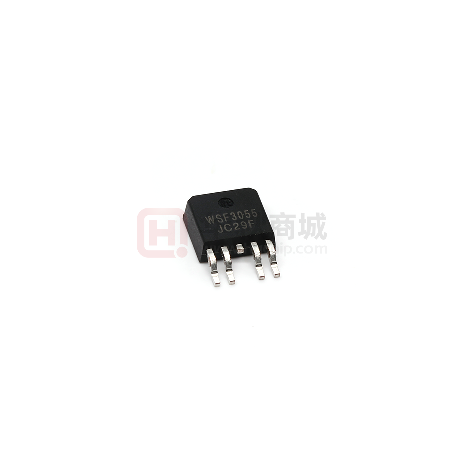
WSF3055
N-Ch and P-Channel MOSFET
Product Summery
Description
The WSF3055 uses advanced trench technology to
VDS
RDS(ON)
ID
provide excellent RDS(ON), low gate charge and
30
15mΩ
24A
operation with gate voltages as low as 4.5V.This device
-30
11mΩ
-19.8A
is suitable for use as a Battery protection or in other
Application
Switching application
Motor Control.
Protable equipment application.
Features
Synchronous Rectification.
1,100 % U IS + Rg Tested
TO-252 Pin Configuration
2,Re liable and Rugged
3,Lead Free Available (RoHS Compliant)
Absolute Maximum Ratings (T= 25°C unless otherwise noted)
Parameter
Symbol
N Channel
P Channel
VDSS
Drain-Source Voltage
30
-30
VGSS
Gate-Source Voltage
±20
±20
TC=25°C
24
-19.8
TC=100°C
15
-12.6
ID
Continuous Drain Current
PD
Maximum Power Dissipation
ID
Continuous Drain Current
IDMa
Pulsed Drain Current
PD
Maximum Power Dissipation
IS
Diode Continuous Forward Current
TJ
Maximum Junction Temperature
TC=25°C
18.9
TC=100°C
7.6
9
-7.6
TA=70°C
7.3
-6
TA=25°C
36
-30.4
2.78
TA=70°C
1.78
TC=25°C
V
A
W
TA=25°C
TA=25°C
Unit
3
A
A
W
-3
A
150
TSTG
Storage Temperature Range
RƟJC
Thermal Resistance-Junction to Case
RƟJAb
Thermal Resistance-Junction to Ambient
°C
-55 to 150
IASc
Avalanche Current, Single pulse
Steady
State
t ≤10s
Steady
State
L=0.1mH
EASc
Avalanche Energy, Single pulse
L=0.1mH
6.6
°C/W
45
°C/W
95
°C/W
13
19
A
8.5
18
mJ
Note a:Pulse width limited by max. junction temperature.
Note b:Surface mounted on 1in2 pad area.
Note c:UIS tested and pulse width limited by maximum junction temperature 150°C(initial temperature Tj=25°C)
www.winsok.tw
Page 1
Rev1.0 May.2020
�WSF3055
N-Ch and P-Channel MOSFET
N Channel Electrical Characteristics (T= 25°C unless otherwise noted)
Symbol
Parameter
Test Conditions
N Channel
Unit
Min.
Typ.
Max.
30
-
-
V
-
-
50
A
-
-
5
mA
1.3
1.8
2.3
V
Static Characteristics
BVDSS
IDSS
VGS(th)
IGSS
RDS(ON) d
Drain-Source Breakdown Voltage VGS=0V, IDS=250μA
Zero Gate Voltage Drain Current
VDS=24V, VGS=0V
Gate Threshold Voltage
VDS=VGS, IDS=250μA
Gate Leakage Current
VGS=±20V, VDS=0V
-
-
±100
nA
VGS=10V, IDS=9A
-
15
20
mΩ
VGS=4.5V, IDS=8A
-
18
23
mΩ
0.3
0.4
0.55
V
-
11
-
ns
-
3.5
-
nC
-
3.3
-
Ω
-
395
514
-
105
-
Drain-Source On-state Resistance
TJ=85°C
Diode Characteristics
VSDd
Diode Forward Voltage
trr
Reverse Recovery Time
Qrr
Reverse Recovery Charge
ISD=1A, VGS=0V
ISD=4.0A, dlSD/dt=100A/μs
Dynamic Characteristics e
RG
Gate Resistance
Ciss
Input Capacitance
VGS=0V,VDS=0V,f=1MHz
VGS=0V, VDS=15V,
Frequency=1.0MHz
Coss
Output Capacitance
Crss
Reverse Transfer Capacitance
-
42
-
td(ON)
Turn-on Delay Time
-
5.5
-
tr
Turn-on Rise Time
-
10.5
-
td(OFF)
Turn-off Delay Time
-
15
-
-
3.7
-
-
4
-
-
8.3
12.5
-
1.1
-
-
1.8
-
tf
VDD=15V, RL=15 , IDS=1A,
VGEN=10V, RG=6
Turn-off Fall Time
pF
ns
Gate Charge Characteristics e
Qg
Total Gate Charge
Qg
Total Gate Charge
Qgs
Gate-Source Charge
Qgd
Gate-Drain Charge
VDS=15V,VGS=4.5V, IDS=4A
VDS=15V, VGS=10V,
IDS=4.0A
nC
Note d:Pulse test ; pulse width:≤300μs, duty cycle≤2%.
Note e:Guaranteed by design, not subject to production testing.
www.winsok.tw
Page 2
Rev1.0 May.2020
�WSF3055
N-Ch and P-Channel MOSFET
N Channel Typical Operating Characteristics
Drain Current
21
28
18
24
15
20
ID - Drain Current (A)
Ptot - Power (W)
Power Dissipation
12
9
6
3
16
12
8
4
o
0
o
TC=25 C
0
20
40
60
0
80 100 120 140 160
0
20
40
60
80 100 120 140 160
TJ - Junction Temperature (°C)
TJ- Junction Temperature (°C)
Safe Operation Area
Thermal Transient Impedance
300
Normalized Transient Thermal Resistance
3
100
ID - Drain Current (A)
TC=25 C,VG=10V
it
m
Li
)
on
s(
Rd
100ms
10
300ms
1ms
10ms
1
DC
o
TC=25 C
0.1
0.1
1
10
0.2
0.1
0.1
0.05
0.02
0.01
0.01
1E-3
Single Pulse
o
1E-4
1E-6
100
VDS - Drain - Source Voltage (V)
www.winsok.tw
Duty = 0.5
1
RqJC :6.6 C/W
1E-5
1E-4
1E-3
0.01
0.1 0.5
Square Wave Pulse Duration (sec)
Page 3
Rev1.0 May.2020
�WSF3055
N-Ch and P-Channel MOSFET
N Channel Typical Operating Characteristics (Cont.)
Output Characteristics
Drain-Source On Resistance
48
40
VGS=4.5,5,6,7,8,9,10V
4V
24
3.5V
16
40
RDS(ON) - On - Resistance (W)
ID - Drain Current (A)
32
8
3V
0
0.0
2.5V
0.5
1.0
1.5
2.0
2.5
16
8
0
5
10
15
20
25
Transfer Characteristics
Gate Threshold Voltage
1.6
Normalized Threshold Voltage
RDS(ON) - On - Resistance (mW)
VGS=10V
ID - Drain Current (A)
60
50
40
30
20
3
4
5
6
7
8
9
30
IDS=250mA
1.4
1.2
1.0
0.8
0.6
0.4
-50 -25
10
VGS - Gate - Source Voltage (V)
www.winsok.tw
24
0
3.0
IDS=9A
2
VGS=4.5V
VDS - Drain-Source Voltage (V)
70
10
32
0
25
50
75 100 125 150
TJ - Junction Temperature (°C)
Page 4
Rev1.0 May.2020
�WSF3055
N-Ch and P-Channel MOSFET
N Channel Typical Operating Characteristics (Cont.)
Drain-Source On Resistance
30
1.8
VGS =10V
IDS =9A
1.6
o
Tj=150 C
10
1.4
IS - Source Current (A)
Normalized On Resistance
Source-Drain Diode Forward
1.2
1.0
0.8
1
o
Tj=25 C
0.6
o
RON@Tj=25 C: 18.5mW
0.4
-50 -25
0
25
50
0.1
0.0
75 100 125 150
0.8
1.0
Capacitance
Gate Charge
VDS=15V
9 I =4A
DS
VGS - Gate - source Voltage (V)
Ciss
400
350
300
250
200
150
1.2
10
Frequency=1MHz
450
C - Capacitance (pF)
0.6
VSD - Source - Drain Voltage (V)
500
Coss
Crss
50
0
0.4
TJ - Junction Temperature (°C)
550
100
0.2
8
7
6
5
4
3
2
1
0
5
10
15
20
0
0.0
25
3.0
4.5
6.0
7.5
9.0
QG - Gate Charge (nC)
VDS - Drain - Source Voltage (V)
www.winsok.tw
1.5
Page 5
Rev1.0 May.2020
�WSF3055
N-Ch and P-Channel MOSFET
P Channel Electrical Characteristics (T= 25°C unless otherwise noted)
Symbol Parameter
P Channel
Test Conditions
Unit
Min.
Typ.
Max.
-30
-
-
-
-
-1
-
-
-30
-1.3
-1.8
-2.3
V
Static Characteristics
BVDSS
IDSS
Drain-Source Breakdown Voltage VGS=0V, IDS=-250μA
Zero Gate Voltage Drain Current
VGS( th) Gate Threshold Voltage
VDS=-24V,
VGS=0V
TJ=85°C
VDS=VGS, IDS=-250μA
V
A
IGSS
Gate Leakage Current
VGS=±20V, VDS=0V
-
-
±100
nA
RDS(ON)d
Drain-Source On-state
Resistance
VGS=-10V, IDS=-7A
-
11
14
mΩ
VGS=-4.5V, IDS=-4A
-
15
20
mΩ
Diode Characteristics
VSDd
Diode Forward Voltage
ISD=-1A, VGS=0V
-
-0.75
-1
V
trr
Reverse Recovery Time
-
17
-
ns
Qrr
Reverse Recovery Charge
ISD=-7.0A,
dlSD/dt=100A/μs
-
9
-
nC
VGS=0V,VDS=0V,f=1MHz
-
12
-
Ω
-
750
975
-
142
-
Dynamic Characteristics e
RG
Gate Resistance
Ciss
Input Capacitance
VGS=0V, VDS=-15V,
Frequency=1.0MHz
Coss
Output Capacitance
Crss
Reverse Transfer Capacitance
-
102
-
td(ON)
Turn-on Delay Time
-
9
17
tr
Turn-on Rise Time
-
11
20
td( OFF)
Turn-off Delay Time
-
55
99
-
34
62
-
8
-
tf
VDD=-15V, RL=15 , IDS=-1A,
VGEN =-10V, RG =6
Turn-off Fall Time
pF
ns
Gate Charge Characteristics e
Qg
Total Gate Charge
VDS=-15V, VGS=-4.5V, IDS=7.0A
Qg
Total Gate Charge
-
17
24
Qgth
Threshold Gate Charge
-
1
-
Qgs
Gate-Source Charge
-
2
-
Qgd
Gate-Drain Charge
-
4
-
VDS=-15V, VGS=-10V, IDS=7.0A
nC
Note d:Pulse test ; pulse width ≤300μs, duty cycle≤2%.
Note e:Guaranteed by design, not subject to production testing.
www.winsok.tw
Page 6
Rev1.0 May.2020
�WSF3055
N-Ch and P-Channel MOSFET
P Channel Typical Operating Characteristics
Power Dissipation
Drain Current
21
24
18
20
-ID - Drain Current (A)
Ptot - Power (W)
15
12
9
6
16
12
8
4
3
o
o
0
TC=25 C
0
20
40
60
40
60
80 100 120 140 160
Safe Operation Area
Thermal Transient Impedance
Normalized Transient Thermal Resistance
-ID - Drain Current (A)
20
TJ - Junction Temperature (°C)
100
it
m
Li
)
on
s(
Rd
100ms
10
300ms
1ms
10ms
1
o
TC=25 C
1
10
3
Duty = 0.5
1
0.2
0.1
0.1
0.05
0.02
0.01
0.01
1E-3
DC
Single Pulse
o
1E-4
1E-6
100
-VDS - Drain - Source Voltage (V)
www.winsok.tw
0
TJ- Junction Temperature (°C)
300
0.1
0.1
0
80 100 120 140 160
TC=25 C,VG=-10V
RqJC :6.6 C/W
1E-5
1E-4
1E-3
0.01
0.1 0.5
Square Wave Pulse Duration (sec)
Page 7
Rev1.0 May.2020
�WSF3055
N-Ch and P-Channel MOSFET
P Channel Typical Operating Characteristics (Cont.)
Output Characteristics
30
Drain-Source On Resistance
60
VGS=-4.5,-5,-6,-7,-8,-9,-10V
-4V
50
RDS(ON) - On - Resistance (W)
-ID - Drain Current (A)
25
20
-3.5V
15
10
-3V
5
0
-2.5V
0
1
2
3
4
30
VGS=-10V
20
10
0
5
VGS=-4.5V
40
0
5
-VDS - Drain - Source Voltage (V)
1.6
IDS=-7A
25
30
IDS=-250mA
1.4
Normalized Threshold Voltage
RDS(ON) - On - Resistance (mW)
20
Gate Threshold Voltage
100
80
60
40
20
0
15
-ID - Drain Current (A)
Transfer Characteristics
120
10
2
3
4
5
6
7
8
9
1.0
0.8
0.6
0.4
0.2
-50 -25
10
-VGS - Gate - Source Voltage (V)
www.winsok.tw
1.2
0
25
50
75 100 125 150
TJ - Junction Temperature (°C)
Page 8
Rev1.0 May.2020
�WSF3055
N-Ch and P-Channel MOSFET
P Channel Typical Operating Characteristics (Cont.)
Drain-Source On Resistance
1.8
30
VGS = -10V
IDS = -7A
1.6
10
1.4
-IS - Source Current (A)
Normalized On Resistance
Source-Drain Diode Forward
1.2
1.0
0.8
o
Tj=150 C
o
Tj=25 C
1
0.6
o
RON@Tj=25 C: 24mW
0.4
-50 -25
0
25
50
0.1
0.0
75 100 125 150
Gate Charge
VDS=-15V
9 I =-7A
DS
-VGS - Gate - source Voltage (V)
C - Capacitance (pF)
800
Ciss
700
600
500
400
300
200
Coss
Crss
5
1.5
10
900
8
7
6
5
4
3
2
1
10
15
20
0
0
25
3
6
9
12
15
18
QG - Gate Charge (nC)
-VDS - Drain - Source Voltage (V)
www.winsok.tw
1.2
Capacitance
Frequency=1MHz
0
0.9
-VSD - Source - Drain Voltage (V)
1000
0
0.6
TJ- Junction Temperature (°C)
1100
100
0.3
Page 9
Rev1.0 May.2020
�Attention�
1,�Any�and�all�Winsok�power�products�described�or�contained�herein�do�not�have�specifications�that�can�handle�
applications�that�require�extremely�high�levels�of�reliability,�such�as�lifeͲsupport�systems,�aircraft's�control�systems,�or�
other�applications�whose�failure�can�be�reasonably�expected�to�result�in�serious�physical�and/or�material�damage.� �
Consult�with�your�Winsok�power�representative�nearest�you�before�using�any�Winsok�power�products�described�or�
contained�herein�in�such�applications.�
2,Winsok�power�assumes�no�responsibility�for�equipment�failures�that�result�from�using�products�at�values�that�exceed,� �
even�momentarily,�rated�values�(such�as�maximum�ratings,�operating�condition�ranges,�or�other�parameters)�listed�in�
products�specifications�of�any�and�all�Winsok�power�products�described�or�contained�herein.�
3,�Specifications�of�any�and�all�Winsok�power�products�described�or�contained�herein�stipulate�the�performance,�
characteristics,�and�functions�of�the�described�products�in�the�independent�state,�and�are�not�guarantees�of�the�
performance,�characteristics,�and�functions�of�the�described�products�as�mounted�in�the�customer’s�products�or�
equipment.�To�verify�symptoms�and�states�that�cannot�be�evaluated�in�an�independent�device,�the�customer�should�always�
evaluate�and�test�devices�mounted�in�the�customer’s�products�or�equipment.�
4,�Winsok�power�Semiconductor�CO.,�LTD.�strives�to�supply�highͲquality�highͲreliability�products.�However,�any�and�all�
semiconductor�products�fail�with�some�probability.�It�is�possible�that�these�probabilistic�failures�could�give�rise�to�accidents�
or�events�that�could�endanger�human�lives�that�could�give�rise�to�smoke�or�fire,�or�that�could�cause�damage�to�other�
property.�When�designing�equipment,�adopt�safety�measures�so�that�these�kinds�of�accidents�or�events�cannot�occur.�Such�
measures�include�but�are�not�limited�to�protective�circuits�and�error�prevention�circuits�for�safe�design,�redundant�design,�
and�structural�design.�
5,In�the�event�that�any�or�all�Winsok�power�products(including�technical�data,�services)�described�or�contained�herein�are�
controlled�under�any�of�applicable�local�export�control�laws�and�regulations,�such�products�must�not�be�exported�without�
obtaining�the�export�license�from�the�authorities�concerned�in�accordance�with�the�above�law.�
6,�No�part�of�this�publication�may�be�reproduced�or�transmitted�in�any�form�or�by�any�means,�electronic�or�mechanical,�
including�photocopying�and�recording,�or�any�information�storage�or�retrieval�system,�or�otherwise,�without�the�prior�
written�permission�of�Winsok�power�Semiconductor�CO.,�LTD.�
7,�Information�(including�circuit�diagrams�and�circuit�parameters)�herein�is�for�example�only;�it�is�not�guaranteed�for�
volume�production. Winsok�power�believes�information�herein�is�accurate�and�reliable,�but�no�guarantees�are�made�or�
implied�regarding�its�use�or�any�infringements�of�intellectual�property�rights�or�other�rights�of�third�parties.�
8,�Any�and�all�information�described�or�contained�herein�are�subject�to�change�without�notice�due�to�product/technology�
improvement,etc.�When�designing�equipment,�refer�to�the�"Delivery�Specification"�for�the�Winsok�power�product�that�you� �
Intend�to�use.�
9,�this�catalog�provides�information�as�of�Sep.2014. Specifications�and�information�herein�are�subject�to�change�without�
notice.�
�


 工商网监
湘ICP备2023018690号
工商网监
湘ICP备2023018690号
