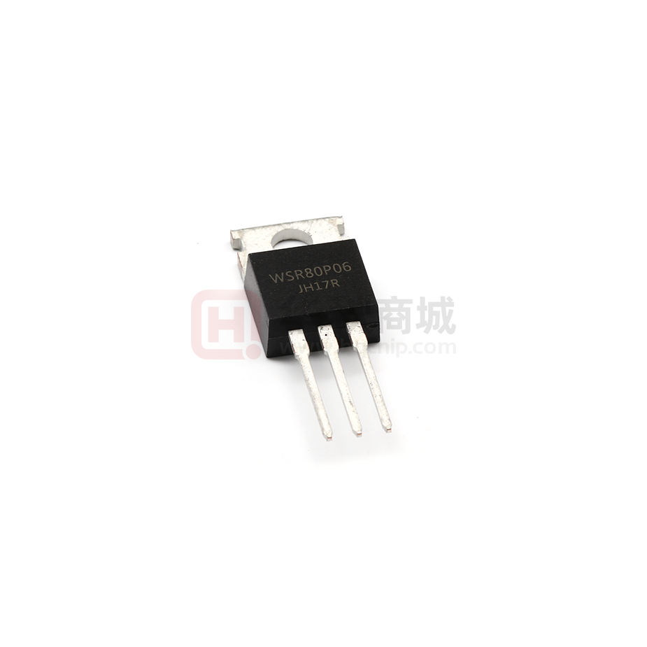
WSR80P06
P-Ch MOSFET
Product Summery
General Description
The WSR80P06 uses advanced trench
technology to provide excellent RDS(ON), low
gate charge and operation with gate voltages as
low as 4.5V. This device is suitable for use as a
Battery protection or in other Switching
application.
BVDSS
RDSON
ID
-60V
18mΩ
-50A
Applications
zBattery protection /Load switch /Uninterruptible
power supply
Features
TO-220AB Pin Configuration
z Super Low Gate Charge
z Excellent CdV/dt effect decline
z 100% EAS Guaranteed
z Green Device Available
Absolute Maximum Ratings
Symbol
Parameter
Rating
Units
VDS
Drain-Source Voltage
-60
V
VGS
Gate-Source Voltage
±20
V
Continuous Drain Current, VGS @ -10V;TC=25°C
-50
A
Continuous Drain Current, VGS @ -10V;TC=100°C
-34
A
Diode Continuous Forward Current
-20
A
Avalanche Energy, Single pulse ;L=1mH
45
A
ID
Is
IAS
EAS
Avalanche Energy, Single pulse;;L=1mH
101
mJ
IDP
Pulse Drain Current Tested ;Tc=25°C
-90
A
Maximum Power Dissipation;TC=25°C
86.8
W
Maximum Power Dissipation;TC=100°C
35
W
TSTG
Storage Temperature Range
-55 to 150
℃
TJ
Operating Junction Temperature Range
-55 to 150
℃
PD
Thermal Data
Symbol
Parameter
Max.
Unit
RθJA
Thermal Resistance Junction-Ambient 1
---
62
℃/W
RθJC
Thermal Resistance Junction-Case1
---
1.44
℃/W
www.winsok.tw
Typ.
Page 1
Rev 1: May.2019
�WSR80P06
P-Ch MOSFET
Electrical Characteristics (TJ=25 ℃, unless otherwise noted)
Symbol
Parameter
BVDSS
Drain-Source Breakdown Voltage
RDS(ON)
Static Drain-Source On-Resistance2
VGS(th)
Gate Threshold Voltage
Conditions
Min.
Typ.
Max.
Unit
VGS=0V , ID=-250uA
-60
---
---
V
VGS=-10V , ID=-18A
---
13
18
VGS=-4.5V , ID=-12A
---
18
25
-1.3
---
-3.0
VGS=VDS , ID =-250uA
mΩ
V
VDS=-48V , VGS=0V , TJ=25℃
---
---
1
VDS=-48V , VGS=0V , TJ=55℃
---
---
5
Gate-Source Leakage Current
VGS=±20V , VDS=0V
---
---
±100
nA
gfs
Forward Transconductance
VDS=-10V , ID=-18A
S
Qg
Total Gate Charge (-4.5V)
Qgs
Gate-Source Charge
Qgd
IDSS
Drain-Source Leakage Current
IGSS
Td(on)
Tr
Td(off)
Tf
Ciss
---
23
---
---
25
---
---
6.7
---
Gate-Drain Charge
---
5.5
---
Turn-On Delay Time
---
38
---
VDS=-20V , VGS=-4.5V , ID=-12A
uA
nC
Rise Time
VDD=-15V , VGS=-10V ,
---
23.6
---
Turn-Off Delay Time
RG=3.3Ω, ID=-1A
---
100
---
---
6.8
---
---
3635
---
---
224
---
---
141
---
Min.
Typ.
Max.
Unit
---
---
-1.2
V
Fall Time
Input Capacitance
VDS=-15V , VGS=0V , f=1MHz
Coss
Output Capacitance
Crss
Reverse Transfer Capacitance
ns
pF
Diode Characteristics
Symbol
VSD
Parameter
2
Diode Forward Voltage
Conditions
VGS=0V , IS=-1A , TJ=25℃
Note :
1.The data tested by surface mounted on a 1 inch2 FR-4 board with 2OZ copper.
2.The data tested by pulsed , pulse width ≦ 300us , duty cycle ≦ 2%
3.The EAS data shows Max. rating . The test condition is V DD=-25V,VGS=-10V,L=0.1mH,IAS=-45A
4.The power dissipation is limited by 150℃ junction temperature
5.The data is theoretically the same as ID and IDM , in real applications , should be limited by total power dissipation.
www.winsok.tw
Page 2
Rev 1: May.2019
�WSR80P06
P-Ch MOSFET
Typical Characteristics
Fig.1 Typical Output Characteristics
Fig.2 On-Resistance vs. G-S Voltage
12
10
VDS=-20V
-VGS Gate to Source Voltage (V)
-IS Source Current(A)
10
8
6
TJ=150℃
TJ=25℃
4
2
0
0.2
0.4
0.6
0.8
ID=-12A
8
6
4
2
0
0
1
Fig.3 Source Drain Forward Characteristics
40
60
Fig.4 Gate-Charge Characteristics
2.0
Normalized On Resistance
1.5
Normalized -VGS(th)
20
QG , Total Gate Charge (nC
-VSD , Source-to-Drain Voltage (V)
1.5
1
1.0
0.5
0.5
0
-50
0
50
100
TJ ,Junction Temperature ( ℃)
-50
150
Fig.5 Normalized VGS(th) vs. TJ
www.winsok.tw
0
50
100
150
TJ , Junction Temperature (℃)
Fig.6 Normalized RDSON vs. TJ
Page 3
Rev 1: May.2019
�WSR80P06
P-Ch MOSFET
Typical Characteristics
10000
100.00
F=1.0MHz
100us
Ciss
Capacitance (pF)
10.00
1ms
10ms
100ms
DC
-ID (A)
1000
1.00
Coss
100
Crss
0.10
Tc=25o C
Single Pulse
0.01
10
1
5
9
13
17
-VDS Drain to Source Voltage(V)
21
0.1
25
Fig.7 Capacitance
1
10
-VDS (V)
100
1000
Fig.8 Safe Operating Area
Normalized Thermal Response (RθJC)
1
DUTY=0.5
0.3
0.1
0.1
0.05
PDM
T
0.02
0.01
0.01
0.00001
TON
D = TON/T
TJpeak = TC + PDM x RθJC
SINGLE PULSE
0.0001
0.001
0.01
0.1
1
10
t , Pulse Width (s)
Fig.9 Normalized Maximum Transient Thermal Impedance
Fig.11 Unclamped Inductive Waveform
Fig.10 Switching Time Waveform
www.winsok.tw
Page 4
Rev 1: May.2019
�Attention�
1,�Any�and�all�Winsok�power�products�described�or�contained�herein�do�not�have�specifications�that�can�handle�
applications�that�require�extremely�high�levels�of�reliability,�such�as�lifeͲsupport�systems,�aircraft's�control�systems,�or�
other�applications�whose�failure�can�be�reasonably�expected�to�result�in�serious�physical�and/or�material�damage.� �
Consult�with�your�Winsok�power�representative�nearest�you�before�using�any�Winsok�power�products�described�or�
contained�herein�in�such�applications.�
2,Winsok�power�assumes�no�responsibility�for�equipment�failures�that�result�from�using�products�at�values�that�exceed,� �
even�momentarily,�rated�values�(such�as�maximum�ratings,�operating�condition�ranges,�or�other�parameters)�listed�in�
products�specifications�of�any�and�all�Winsok�power�products�described�or�contained�herein.�
3,�Specifications�of�any�and�all�Winsok�power�products�described�or�contained�herein�stipulate�the�performance,�
characteristics,�and�functions�of�the�described�products�in�the�independent�state,�and�are�not�guarantees�of�the�
performance,�characteristics,�and�functions�of�the�described�products�as�mounted�in�the�customer’s�products�or�
equipment.�To�verify�symptoms�and�states�that�cannot�be�evaluated�in�an�independent�device,�the�customer�should�always�
evaluate�and�test�devices�mounted�in�the�customer’s�products�or�equipment.�
4,�Winsok�power�Semiconductor�CO.,�LTD.�strives�to�supply�highͲquality�highͲreliability�products.�However,�any�and�all�
semiconductor�products�fail�with�some�probability.�It�is�possible�that�these�probabilistic�failures�could�give�rise�to�accidents�
or�events�that�could�endanger�human�lives�that�could�give�rise�to�smoke�or�fire,�or�that�could�cause�damage�to�other�
property.�When�designing�equipment,�adopt�safety�measures�so�that�these�kinds�of�accidents�or�events�cannot�occur.�Such�
measures�include�but�are�not�limited�to�protective�circuits�and�error�prevention�circuits�for�safe�design,�redundant�design,�
and�structural�design.�
5,In�the�event�that�any�or�all�Winsok�power�products(including�technical�data,�services)�described�or�contained�herein�are�
controlled�under�any�of�applicable�local�export�control�laws�and�regulations,�such�products�must�not�be�exported�without�
obtaining�the�export�license�from�the�authorities�concerned�in�accordance�with�the�above�law.�
6,�No�part�of�this�publication�may�be�reproduced�or�transmitted�in�any�form�or�by�any�means,�electronic�or�mechanical,�
including�photocopying�and�recording,�or�any�information�storage�or�retrieval�system,�or�otherwise,�without�the�prior�
written�permission�of�Winsok�power�Semiconductor�CO.,�LTD.�
7,�Information�(including�circuit�diagrams�and�circuit�parameters)�herein�is�for�example�only;�it�is�not�guaranteed�for�
volume�production. Winsok�power�believes�information�herein�is�accurate�and�reliable,�but�no�guarantees�are�made�or�
implied�regarding�its�use�or�any�infringements�of�intellectual�property�rights�or�other�rights�of�third�parties.�
8,�Any�and�all�information�described�or�contained�herein�are�subject�to�change�without�notice�due�to�product/technology�
improvement,etc.�When�designing�equipment,�refer�to�the�"Delivery�Specification"�for�the�Winsok�power�product�that�you� �
Intend�to�use.�
9,�this�catalog�provides�information�as�of�Sep.2014. Specifications�and�information�herein�are�subject�to�change�without�
notice.�
�


 工商网监
湘ICP备2023018690号
工商网监
湘ICP备2023018690号
