CH3D06065A
Silicon Carbide Schottky Diode
Features
650
V
IF ( TC≤135℃) =
9
A
=
18
nC
VRRM
QC
=
Package
Zero Reverse Recovery Current
Zero Forward Recovery Voltage
Positive Temperature Coefficient on VF
Temperature-independent Switching
175°C Operating Junction Temperature
Benefits
TO-220-2
Replace Bipolar with Unipolar Device
Reduction of Heat Sink Size
Parallel Devices Without Thermal Runaway
Essentially No Switching Losses
Applications
Switch Mode Power Supplies
Power Factor Correction
Motor drive, PV Inverter, Wind Power Station
Part Number
Package
Marking
CH3D06065A
TO-220-2
CH3D06065A
Maximum Ratings
Symbol
Parameter
Value
Unit
Test Conditions
VRRM
Repetitive Peak Reverse Voltage
650
V
TC = 25℃
VRSM
Surge Peak Reverse Voltage
650
V
TC = 25℃
DC Blocking Voltage
650
V
TC = 25℃
Forward Current
19
9
6
A
TC ≤ 25℃
TC ≤ 135℃
VR
IF
TC ≤ 155℃
IFSM
Non-Repetitive Forward Surge Current
60
A
TC = 25℃, tp = 8.3ms, Half Sine Wave
Ptot
Power Dissipation
93
W
TC = 25℃
TC
Maximum Case Temperature
155
℃
-55 to
175
℃
1
Nm
TJ,TSTG
Operating Junction and Storage Temperature
TO-220 Mounting Torque
Note
1
M3 Screw
Fig.3
�Electrical Characteristics
Symbol
Parameter
VF
Forward Voltage
IR
Reverse Current
Typ.
Max.
1.4
1.65
1.75
2.3
1
20
5
100
Unit
V
µA
300
C
Total Capacitance
34
Total Capacitive Charge
18
IF = 6A, TJ = 25℃
Note
Fig.1
IF = 6A, TJ = 175℃
VR = 650V, TJ = 25℃
VR = 650V, TJ = 175℃
Fig.2
VR = 0V, TJ = 25℃, f = 1MHz
/
pF
VR = 200V, TJ = 25℃, f = 1MHz
Fig.5
VR = 400V, TJ = 25℃, f = 1MHz
30
QC
Test Conditions
/
nC
VR = 650V, IF = 6A
di/dt = 200A/µs, TJ = 25℃
Fig.4
Thermal Characteristics
Symbol
Parameter
Typ.
Unit
Note
Fig.6
RθJC
Thermal Resistance from Junction to Case
1.6
℃/W
RθJA
Thermal Resistance from Junction to Ambient
80
℃/W
Tsold
Soldering Temperature
260
℃
IF (A)
IR (μA)
Typical Performance
VF (V)
VR (V)
2
�QC (nC)
PTot (W)
Typical Performance
VR (V)
TC (℃)
Figure 4. Total Capacitive Charge vs. Reverse Voltage
C (pF)
Thermal Resistance(℃/W)
Figure 3. Power Derating
VR (V)
T(sec)
Figure 5. Total Capacitance vs. Reverse Voltage
Figure 6. Transient Thermal Impedance
3
�Package Dimensions
Package TO-220-2
Symbol
Min. (mm)
Typ. (mm)
Max. (mm)
A
9.17
10.08
10.91
B
27.00
28.58
30.00
C
3.89
4.50
5.00
D
4.20
5.10
5.80
E
11.70
13.30
14.97
F
0.50
0.80
1.21
Simplified Diode Model
Equivalent IV Curve for Model
Mathematical Equation
VF=Vt + IF×Rdiff
IF=f(VF)
Vt = -0.0017×Tj + 1.0298 [V]
Rdiff = 2×10⁻⁶×Tj2 + 2×10⁻⁴×Tj + 0.0802 [Ω]
Note:
Tj = Diode Junction Temperature In Degrees Celsius,
valid from 25°C to 175°C
IF= Forward Current
Less than 12A
4
�
很抱歉,暂时无法提供与“CH3D06065A”相匹配的价格&库存,您可以联系我们找货
免费人工找货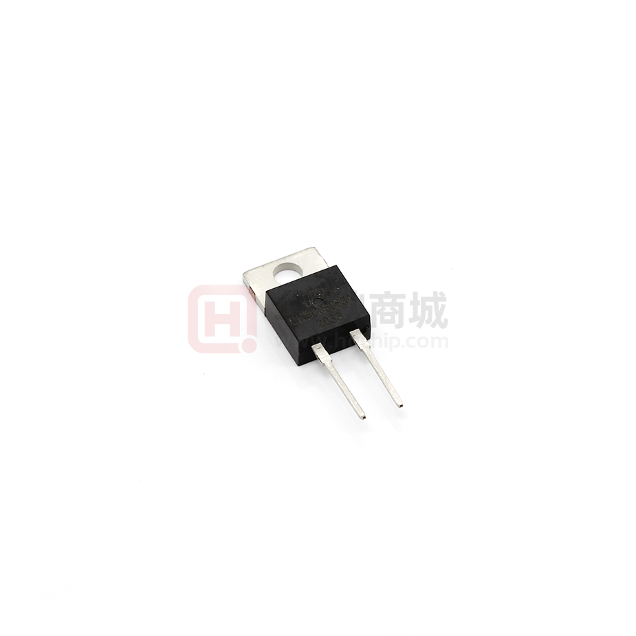


 工商网监
湘ICP备2023018690号
工商网监
湘ICP备2023018690号

