LM723, LM723C
www.ti.com
SNVS765C – JUNE 1999 – REVISED APRIL 2013
LM723/LM723C Voltage Regulator
Check for Samples: LM723, LM723C
FEATURES
DESCRIPTION
•
The LM723/LM723C is a voltage regulator designed
primarily for series regulator applications. By itself, it
will supply output currents up to 150 mA; but external
transistors can be added to provide any desired load
current. The circuit features extremely low standby
current drain, and provision is made for either linear
or foldback current limiting.
1
2
•
•
•
•
150 mA Output Current Without External Pass
Transistor
Output Currents in Excess of 10A Possible by
Adding External Transistors
Input Voltage 40V Max
Output Voltage Adjustable from 2V to 37V
Can be Used as Either a Linear or a Switching
Regulator
The LM723/LM723C is also useful in a wide range of
other applications such as a shunt regulator, a
current regulator or a temperature controller.
The LM723C is identical to the LM723 except that the
LM723C has its performance ensured over a 0°C to
+70°C temperature range, instead of −55°C to
+125°C.
Connection Diagram
Note: Pin 5 connected to case.
Figure 1. Top View
CDIP Package or PDIP Package
See Package J or NFF0014A
Figure 2. Top View
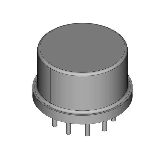
TO-100
See Package LME
Figure 3. Top View
See Package NAJ0020A
1
2
Please be aware that an important notice concerning availability, standard warranty, and use in critical applications of
Texas Instruments semiconductor products and disclaimers thereto appears at the end of this data sheet.
All trademarks are the property of their respective owners.
PRODUCTION DATA information is current as of publication date.
Products conform to specifications per the terms of the Texas
Instruments standard warranty. Production processing does not
necessarily include testing of all parameters.
Copyright © 1999–2013, Texas Instruments Incorporated
�LM723, LM723C
SNVS765C – JUNE 1999 – REVISED APRIL 2013
www.ti.com
Equivalent Circuit*
*Pin numbers refer to metal can package.
Typical Application
for minimum temperature drift.
Typical Performance
Regulated Output Voltage
5V
Line Regulation (ΔVIN = 3V)
0.5mV
Load Regulation (ΔIL = 50 mA)
1.5mV
Figure 4. Basic Low Voltage Regulator (VOUT = 2 to 7 Volts)
2
Submit Documentation Feedback
Copyright © 1999–2013, Texas Instruments Incorporated
Product Folder Links: LM723 LM723C
�LM723, LM723C
www.ti.com
SNVS765C – JUNE 1999 – REVISED APRIL 2013
These devices have limited built-in ESD protection. The leads should be shorted together or the device placed in conductive foam
during storage or handling to prevent electrostatic damage to the MOS gates.
ABSOLUTE MAXIMUM RATINGS (1) (2)
Pulse Voltage from V+ to V− (50 ms)
50V
Continuous Voltage from V+ to V−
40V
Input-Output Voltage Differential
40V
Maximum Amplifier Input Voltage
(Either Input)
8.5V
Maximum Amplifier Input Voltage
(Differential)
5V
Current from VZ
25 mA
Current from VREF
15 mA
Internal Power Dissipation
Metal Can (3)
800 mW
CDIP
(3)
900 mW
PDIP
(3)
660 mW
Operating Temperature Range
−55°C to +150°C
LM723
LM723C
0°C to +70°C
Storage Temperature Range
Metal Can
−65°C to +150°C
−55°C to +150°C
PDIP
Lead Temperature (Soldering, 4 sec. max.)
Hermetic Package
300°C
Plastic Package
260°C
ESD Tolerance
1200V
(Human body model, 1.5 kΩ in series with 100 pF)
(1)
(2)
(3)
“Absolute Maximum Ratings” indicate limits beyond which damage to the device may occur. Operating Ratings indicate conditions for
which the device is functional, but do not ensure specific performance limits.
A military RETS specification is available on request. At the time of printing, the LM723 RETS specification complied with the Min and
Max limits in this table. The LM723E, H, and J may also be procured as a Standard Military Drawing.
See derating curves for maximum power rating above 25°C.
ELECTRICAL CHARACTERISTICS (1) (2) (3) (4)
Parameter
Conditions
LM723
Min
Line Regulation
VIN = 12V to VIN = 15V
LM723C
Typ
Max
0.01
0.1
−55°C ≤ TA ≤ +125°C
Min
Max
0.01
0.1
0.3
(2)
(3)
(4)
% VOUT
0.02
0.2
0.1
0.5
% VOUT
IL = 1 mA to IL = 50 mA
0.03
0.15
0.03
0.2
% VOUT
0.6
% VOUT
0°C ≤ TA ≤ +70°C
(1)
0.3
VIN = 12V to VIN = 40V
−55°C ≤ TA ≤ +125°C
Ripple Rejection
% VOUT
% VOUT
0°C ≤ TA ≤ +70°C
Load Regulation
Units
Typ
0.6
% VOUT
f = 50 Hz to 10 kHz, CREF = 0
74
74
dB
f = 50 Hz to 10 kHz, CREF = 5 μF
86
86
dB
Unless otherwise specified, TA = 25°C, VIN = V+ = VC = 12V, V− = 0, VOUT = 5V, IL = 1 mA, RSC = 0, C1 = 100 pF, CREF = 0 and divider
impedance as seen by error amplifier ≤ 10 kΩ connected as shown in Figure 4. Line and load regulation specifications are given for the
condition of constant chip temperature. Temperature drifts must be taken into account separately for high dissipation conditions.
A military RETS specification is available on request. At the time of printing, the LM723 RETS specification complied with the Min and
Max limits in this table. The LM723E, H, and J may also be procured as a Standard Military Drawing.
Specified by correlation to other tests.
L1 is 40 turns of No. 20 enameled copper wire wound on Ferroxcube P36/22-3B7 pot core or equivalent with 0.009 in. air gap.
Submit Documentation Feedback
Copyright © 1999–2013, Texas Instruments Incorporated
Product Folder Links: LM723 LM723C
3
�LM723, LM723C
SNVS765C – JUNE 1999 – REVISED APRIL 2013
www.ti.com
ELECTRICAL CHARACTERISTICS(1)(2)(3)(4) (continued)
Parameter
Conditions
LM723
Min
Average Temperature Coefficient of
Output Voltage ( (5))
−55°C ≤ TA ≤ +125°C
LM723C
Typ
Max
0.002
0.015
Min
Reference Voltage
Output Noise Voltage
0.003
RSC = 10Ω, VOUT = 0
65
6.95
0.015
65
7.35
6.80
7.15
%/°C
mA
7.50
V
μVrms
BW = 100 Hz to 10 kHz, CREF = 0
86
86
BW = 100 Hz to 10 kHz, CREF = 5 μF
2.5
2.5
μVrms
0.05
0.05
%/1000
hrs
Long Term Stability
Standby Current Drain
7.15
Units
Max
%/°C
0°C ≤ TA ≤ +70°C
Short Circuit Current Limit
Typ
4.0
mA
Input Voltage Range
IL = 0, VIN = 30V
9.5
40
9.5
40
V
Output Voltage Range
2.0
37
2.0
37
V
3.0
38
3.0
Input-Output Voltage Differential
1.7
3.5
1.7
38
V
θJA
PDIP
θJA
CDIP
150
θJA
H10C Board Mount in Still Air
165
165
°C/W
θJA
H10C Board Mount in 400 LF/Min Air Flow
66
66
°C/W
22
22
°C/W
105
θJC
(5)
4
°C/W
°C/W
For metal can applications where VZ is required, an external 6.2V zener diode should be connected in series with VOUT.
Submit Documentation Feedback
Copyright © 1999–2013, Texas Instruments Incorporated
Product Folder Links: LM723 LM723C
�LM723, LM723C
www.ti.com
SNVS765C – JUNE 1999 – REVISED APRIL 2013
TYPICAL PERFORMANCE CHARACTERISTICS
Load Regulation
Characteristics with
Current Limiting
Load Regulation
Characteristics with
Current Limiting
Figure 5.
Figure 6.
Load & Line Regulation vs
Input-Output Voltage
Differential
Current Limiting
Characteristics
Figure 7.
Figure 8.
Current Limiting
Characteristics vs
Junction Temperature
Standby Current Drain vs
Input Voltage
Figure 9.
Figure 10.
Submit Documentation Feedback
Copyright © 1999–2013, Texas Instruments Incorporated
Product Folder Links: LM723 LM723C
5
�LM723, LM723C
SNVS765C – JUNE 1999 – REVISED APRIL 2013
www.ti.com
TYPICAL PERFORMANCE CHARACTERISTICS (continued)
Line Transient Response
Load Transient Response
Figure 11.
Figure 12.
Output Impedence vs
Frequency
Figure 13.
6
Submit Documentation Feedback
Copyright © 1999–2013, Texas Instruments Incorporated
Product Folder Links: LM723 LM723C
�LM723, LM723C
www.ti.com
SNVS765C – JUNE 1999 – REVISED APRIL 2013
MAXIMUM POWER RATINGS
Noise
vs
Filter Capacitor
(CREF in Circuit of Figure 4)
(Bandwidth 100 Hz to 10 kHz)
LM723
Power Dissipation vs
Ambient Temperature
Figure 14.
Figure 15.
LM723C
Power Dissipation vs
Ambient Temperature
Figure 16.
Submit Documentation Feedback
Copyright © 1999–2013, Texas Instruments Incorporated
Product Folder Links: LM723 LM723C
7
�LM723, LM723C
SNVS765C – JUNE 1999 – REVISED APRIL 2013
www.ti.com
Table 1. Resistor Values (kΩ) for Standard Output Voltage
Positive
Output
Voltage
(1)
(2)
(3)
Applicable Figures
Fixed
Output ±5%
Output
Adjustable
±10% (1)
Negative
Output
Voltage
See (2)
R1
R2
R1
P1
R2
+3.0
Figure 4, Figure 19,
Figure 21, Figure 24,
Figure 27 (Figure 19)
4.12
3.01
1.8
0.5
1.2
+100
+3.6
Figure 4, Figure 19,
Figure 21, Figure 24,
Figure 27 (Figure 19)
3.57
3.65
1.5
0.5
1.5
+5.0
Figure 4, Figure 19,
Figure 21, Figure 24,
Figure 27 (Figure 19)
2.15
4.99
0.75
0.5
+6.0
Figure 4, Figure 19,
Figure 21, Figure 24,
Figure 27 (Figure 19)
1.15
6.04
0.5
+9.0
Figure 17, Figure 19,
(Figure 19, Figure 21,
Figure 24, Figure 27)
1.87
7.15
+12
Figure 17, Figure 19,
(Figure 19, Figure 21,
Figure 24, Figure 27)
4.87
+15
Figure 17, Figure 19,
(Figure 19, Figure 21,
Figure 24, Figure 27)
+28
Applicable
Figures
Fixed
Output ±5%
5% Output
Adjustable
±10%
R1
R2
R1
P1
R2
Figure 22
3.57
102
2.2
10
91
+250
Figure 22
3.57
255
2.2
10
240
2.2
−6 (3)
Figure 18,
(Figure 25)
3.57
2.43
1.2
0.5
0.75
0.5
2.7
−9
Figure 18,
Figure 25
3.48
5.36
1.2
0.5
2.0
0.75
1.0
2.7
−12
Figure 18,
Figure 25
3.57
8.45
1.2
0.5
3.3
7.15
2.0
1.0
3.0
−15
Figure 18,
Figure 25
3.65
11.5
1.2
0.5
4.3
7.87
7.15
3.3
1.0
3.0
−28
Figure 18,
Figure 25
3.57
24.3
1.2
0.5
10
Figure 17, Figure 19,
(Figure 19, Figure 21,
Figure 24, Figure 27)
21.0
7.15
5.6
1.0
2.0
−45
Figure 23
3.57
41.2
2.2
10
33
+45
Figure 22
3.57
48.7
2.2
10
39
−100
Figure 23
3.57
97.6
2.2
10
91
+75
Figure 22
3.57
78.7
2.2
10
68
−250
Figure 23
3.57
249
2.2
10
240
Replace R1/R2 in figures with divider shown in Figure 28.
Figures in parentheses may be used if R1/R2 divider is placed on opposite input of error amp.
V+ and VCC must be connected to a +3V or greater supply.
Table 2. Formulae for Intermediate Output Voltages
8
Outputs from +2 to +7 volts
Outputs from +4 to +250 volts
(Figure 4 Figure 19 Figure 20
Figure 21 Figure 24 Figure 27
(Figure 22)
Outputs from +7 to +37 volts
Outputs from −6 to −250 volts
(Figure 17 Figure 19 Figure 20
Figure 21 Figure 24 Figure 27)
(Figure 18 Figure 23 Figure 25)
Submit Documentation Feedback
Current Limiting
Foldback Current Limiting
Copyright © 1999–2013, Texas Instruments Incorporated
Product Folder Links: LM723 LM723C
�LM723, LM723C
www.ti.com
SNVS765C – JUNE 1999 – REVISED APRIL 2013
TYPICAL APPLICATIONS
for minimum temperature drift.
R3 may be eliminated for minimum component count.
Typical Performance
Regulated Output Voltage
15V
Line Regulation (ΔVIN = 3V)
1.5 mV
Load Regulation (ΔIL = 50 mA)
4.5 mV
Figure 17. Basic High Voltage Regulator (VOUT = 7 to 37 Volts)
Typical Performance
Regulated Output Voltage
−15V
Line Regulation (ΔVIN = 3V)
1 mV
Load Regulation (ΔIL = 100 mA)
2 mV
Figure 18. Negative Voltage Regulator
Submit Documentation Feedback
Copyright © 1999–2013, Texas Instruments Incorporated
Product Folder Links: LM723 LM723C
9
�LM723, LM723C
SNVS765C – JUNE 1999 – REVISED APRIL 2013
www.ti.com
Typical Performance
Regulated Output Voltage
+15V
Line Regulation (ΔVIN = 3V)
1.5 mV
Load Regulation (ΔIL = 1A)
15 mV
Figure 19. Positive Voltage Regulator (External NPN Pass Transistor)
Typical Performance
Regulated Output Voltage
+5V
Line Regulation (ΔVIN = 3V)
0.5 mV
Load Regulation (ΔIL = 1A)
5 mV
Figure 20. Positive Voltage Regulator (External PNP Pass Transistor)
10
Submit Documentation Feedback
Copyright © 1999–2013, Texas Instruments Incorporated
Product Folder Links: LM723 LM723C
�LM723, LM723C
www.ti.com
SNVS765C – JUNE 1999 – REVISED APRIL 2013
Typical Performance
Regulated Output Voltage
+5V
Line Regulation (ΔVIN = 3V)
0.5 mV
Load Regulation (ΔIL = 10 mA)
1 mV
Short Circuit Current
20 mA
Figure 21. Foldback Current Limiting
Typical Performance
Regulated Output Voltage
+50V
Line Regulation (ΔVIN = 20V)
15 mV
Load Regulation (ΔIL = 50 mA)
20 mV
Figure 22. Positive Floating Regulator
Submit Documentation Feedback
Copyright © 1999–2013, Texas Instruments Incorporated
Product Folder Links: LM723 LM723C
11
�LM723, LM723C
SNVS765C – JUNE 1999 – REVISED APRIL 2013
www.ti.com
Typical Performance
Regulated Output Voltage
−100V
Line Regulation (ΔVIN = 20V)
30 mV
Load Regulation (ΔIL = 100 mA)
20 mV
Figure 23. Negative Floating Regulator
Typical Performance
Regulated Output Voltage
+5V
Line Regulation (ΔVIN = 30V)
10 mV
Load Regulation (ΔIL = 2A)
80 mV
Figure 24. Positive Switching Regulator
12
Submit Documentation Feedback
Copyright © 1999–2013, Texas Instruments Incorporated
Product Folder Links: LM723 LM723C
�LM723, LM723C
www.ti.com
SNVS765C – JUNE 1999 – REVISED APRIL 2013
Typical Performance
Regulated Output Voltage
−15V
Line Regulation (ΔVIN = 20V)
8 mV
Load Regulation (ΔIL = 2A)
6 mV
Figure 25. Negative Switching Regulator
Note: Current limit transistor may be used for shutdown if current limiting is not required.
Typical Performance
Regulated Output Voltage
+5V
Line Regulation (ΔVIN = 3V)
0.5 mV
Load Regulation (ΔIL = 50 mA)
1.5 mV
Figure 26. Remote Shutdown Regulator with Current Limiting
Submit Documentation Feedback
Copyright © 1999–2013, Texas Instruments Incorporated
Product Folder Links: LM723 LM723C
13
�LM723, LM723C
SNVS765C – JUNE 1999 – REVISED APRIL 2013
www.ti.com
Regulated Output Voltage
+5V
Line Regulation (ΔVIN = 10V)
0.5 mV
Load Regulation (ΔIL = 100 mA)
1.5 mV
Figure 27. Shunt Regulator
Figure 28. Output Voltage Adjust
(1)
14
(1)
Replace R1/R2 in figures with divider shown in Figure 28.
Submit Documentation Feedback
Copyright © 1999–2013, Texas Instruments Incorporated
Product Folder Links: LM723 LM723C
�LM723, LM723C
www.ti.com
SNVS765C – JUNE 1999 – REVISED APRIL 2013
Schematic Diagram
Submit Documentation Feedback
Copyright © 1999–2013, Texas Instruments Incorporated
Product Folder Links: LM723 LM723C
15
�LM723, LM723C
SNVS765C – JUNE 1999 – REVISED APRIL 2013
www.ti.com
REVISION HISTORY
Changes from Revision B (April 2013) to Revision C
•
16
Page
Changed layout of National Data Sheet to TI format .......................................................................................................... 15
Submit Documentation Feedback
Copyright © 1999–2013, Texas Instruments Incorporated
Product Folder Links: LM723 LM723C
�PACKAGE OPTION ADDENDUM
www.ti.com
29-Aug-2018
PACKAGING INFORMATION
Orderable Device
Status
(1)
Package Type Package Pins Package
Drawing
Qty
Eco Plan
Lead/Ball Finish
MSL Peak Temp
(2)
(6)
(3)
Op Temp (°C)
Device Marking
(4/5)
LM723CH
ACTIVE
TO-100
LME
10
500
TBD
Call TI
Call TI
0 to 70
( LM723CH, LM723CH
)
LM723CH/NOPB
ACTIVE
TO-100
LME
10
500
Green (RoHS
& no Sb/Br)
Call TI
Level-1-NA-UNLIM
0 to 70
( LM723CH, LM723CH
)
LM723H
ACTIVE
TO-100
LME
10
500
TBD
Call TI
Call TI
-55 to 150
( LM723H, LM723H)
LM723H/NOPB
ACTIVE
TO-100
LME
10
500
Green (RoHS
& no Sb/Br)
Call TI
Level-1-NA-UNLIM
-55 to 150
( LM723H, LM723H)
(1)
The marketing status values are defined as follows:
ACTIVE: Product device recommended for new designs.
LIFEBUY: TI has announced that the device will be discontinued, and a lifetime-buy period is in effect.
NRND: Not recommended for new designs. Device is in production to support existing customers, but TI does not recommend using this part in a new design.
PREVIEW: Device has been announced but is not in production. Samples may or may not be available.
OBSOLETE: TI has discontinued the production of the device.
(2)
RoHS: TI defines "RoHS" to mean semiconductor products that are compliant with the current EU RoHS requirements for all 10 RoHS substances, including the requirement that RoHS substance
do not exceed 0.1% by weight in homogeneous materials. Where designed to be soldered at high temperatures, "RoHS" products are suitable for use in specified lead-free processes. TI may
reference these types of products as "Pb-Free".
RoHS Exempt: TI defines "RoHS Exempt" to mean products that contain lead but are compliant with EU RoHS pursuant to a specific EU RoHS exemption.
Green: TI defines "Green" to mean the content of Chlorine (Cl) and Bromine (Br) based flame retardants meet JS709B low halogen requirements of


 工商网监
湘ICP备2023018690号
工商网监
湘ICP备2023018690号
