A PERFECT ALLIANCE.
ODU MINI-SNAP®
Miniature circular connectors
with Push-Pull locking.
SERIES L / K / B
ODU MINI-SNAP® L / K / B
ODU MINI-SNAP® F
ODU AMC®
ODU MEDI-SNAP®
ODU MINI-SNAP® PC
www.odu-usa.com
�ODU MINI-SNAP ® L / K / B
TABLE OF CONTENTS
THE ODU CORPORATE GROUP
FEATURES
•
•
•
•
•
•
•
•
Quick and easy mating and demating
�Blind mating and demating in difficult-to-reach places
Low space requirements on the receptacles
Definite and secure locking conditions
�Robotic mating and demating possible
�Easy cleaning of the connector plug housing possible
�High connector density
�Low power requirement
APPLICATIONS
•
•
•
•
•
•
Medical
Industrial
Test and measurement
Military and security
Energy
eMobility
4
PRODUCT INFORMATION
10
Push-Pull connector series at a glance
Specific attributes of series L, K and B
Functional principle of the Push-Pull locking
Facts & figures
12
13
14
15
CONFIGURATION GUIDELINE
16
Correct configuring – step by step
18
ODU MINI-SNAP® SERIES L
22
Summary ODU MINI-SNAP® series L
The LP locking principle
Styles
Keyings
Contact inserts and PCB layouts
Cable collet system
Accessories
24
26
28
39
40
64
66
ODU MINI-SNAP® SERIES K
74
Summary ODU MINI-SNAP® series K
The LP locking principle
Styles
Keyings
Contact inserts and PCB layouts
Cable collet system
Accessories
76
78
80
88
90
108
110
ODU MINI-SNAP® SERIES B
114
Summary ODU MINI-SNAP® series B
The FP locking principle
Styles
Keyings
Contact inserts and PCB layouts
Cable collet system
Accessories
116
118
120
125
126
144
146
TOOLS, CRIMP INFORMATION, PROCESSING INSTRUCTIONS, ACCESSORIES
All shown connectors are according to IEC 61984:2008
(VDE 0627:2009); connectors without breaking capacity (COC).
ODU MINI-SNAP is UL-approved under file E110586.
MIL specification: Tests carried out (see page 170).
All dimensions are in mm.
Some figures are for illustrative purposes only.
Subject to change without notice. Errors and omissions excepted.
We reserve the right to change our products and their technical
specifications at any time in the interest of technical improvement.
This publication supersedes all prior publications.
This publication is also available as a PDF file that can be downloaded from www.odu-usa.com.
Issue: 2018-04
2
Data transmission protocols
These ODU specific connectors can transmit common data transmission protocols
such as USB® 2.0, USB® 3.1 Gen1, CAT 5, CAT 6A and Ethernet , but they are not
USB®-, CAT- and Ethernet-standard connectors.
Crimping tools /assembly tools
Spanner wrench
Nutdriver for slotted mounting nut
Removal tools for crimp-clip-contacts
154
156
158
158
159
TECHNICAL INFORMATION
160
International protection classes acc. IEC 60529:2013 (VDE 0470-1:2014)
Principle of watertightness
Housing materials and insulator materials
Termination technologies
Conversions / AWG
Current load of turned contacts
Operating voltage
Electro magnetic compatibility (EMC)
Autoclaving
Test standard
Technical terms
162
163
164
165
166
167
168
169
170
170
171
For assembly instructions, please refer to our website: www.odu-usa.com/downloads/
Table of Contents
3
�A PERFECT
ALLIANCE.
ODU WORLDWIDE
ODU Scandinavia AB
ODU-USA, Inc.
ODU GmbH & Co. KG
Headquarters
ODU Denmark ApS
ODU North American Logistics
CREATING CONNECTIONS, BUILDING ALLIANCES, COLLABORATING INTO THE FUTURE: WHETHER TWO TECHNICAL COMPONENTS COME TOGETHER TO FORM A UNIT OR PEOPLE COME
TOGETHER TO STRIVE FOR GREAT RESULTS – THE KEY IS TO
ASPIRE IN ACHIEVING SUPERB RESULTS. THIS GOAL DRIVES OUR
WORK. PERFECT CONNECTIONS THAT INSPIRE AND DELIVER
ON THE PROMISES.
ODU (Shanghai)
International Trading Co., Ltd.
ODU Japan K.K.
ODU Mexico
Manufacturing S.R.L. de C.V.
ODU Romania Manufacturing S.R.L.
ODU Italia S.R.L.
ODU France SARL
ODU-UK Ltd.
ODU GROUP OVERVIEW
CERTIFIED QUALITY
• More than 75 years of experience in connector technology
• DIN EN ISO 9001
• A turnover of 170 million Euro
• ISO/TS 16949
• Over 1,900 employees worldwide
• DIN EN ISO 14001
• 9 sales subsidiaries in China, Denmark, France, Germany,
Italy, Japan, Sweden, the UK and the US as well as
5 production and logistics sites
• ISO 13485
• All technologies under one roof: Design and development,
machine tool and special machine construction, injection,
stamping, turning, surface technology, assembly and
cable assembly
As of February 2018
• Wide range of UL, CSA, VG and DVA licenses
• UL certified cable assembly
For a complete list of our certifications, please visit our website.
�THE ODU GROUP
INGENIOUS IDEAS
PERFECT SOLUTIONS
ODU’S PRODUCT PORTFOLIO.
Versatile connector solutions for transmission of power, signals, data,
or media – ODU never fails to offer the right interface when quality and
absolute reliability are the top priorities.
COMPACT MODULAR CONNECTOR SOLUTIONS
PUSH-PULL CIRCULAR CONNECTORS
ELECTRICAL CONTACTS
•
•
•
•
•
•
•
• Circular connector series in robust
metal or plastic housing
• Contacts for soldering, crimping and
PCB termination
• Optional selectable Push-Pull locking ensuring
a secure connection at all times as well as
easy to release Break-Away function
• 2 up to 55 contacts
• IP 50 to IP 69
• Autoclavable for medical applications
• Hybrid inserts for combined transmission
•
•
•
•
Application-specific hybrid interface
For manual mating and automatic docking
The highest packing density
Flexible modular construction
Multitude of data transmission modules
Variety of locking options available
For the transmission of signals, power, high
current, high voltage, coax, high-speed data,
fiber optics and other media such as air or fluid.
• Mating cycles scalable as required
from 10,000 to over 100,000 (1 million)
Versatile connector technologies
Outstanding reliability, lifetime and durability
Up to 1 million mating cycles
Current-carrying capacity of up to
2,400 amperes and more
• Rugged contact systems, suitable even
for harsh environments
• Economical solutions for automatic processing
HEAVY-DUTY & DOCKING
AND ROBOTIC CONNECTOR SOLUTIONS
APPLICATION AND
CUSTOMER-SPECIFIC SOLUTIONS
CABLE ASSEMBLY
• Extremely durable even under extreme / harsh
environments
• Interference-free and secure connection,
even under vibration
• Up to 500 A (higher currents upon request)
• High contact security due to the springwire
technology
• High pin density due to a minimum contact
diameter
• Low contact resistance
• Contacts, connectors and assemblies for
the highest technical requirements as well
as special applications
• First-class implementation expertise
• High level of vertical manufacturing –
all competences and key technologies
under one roof
• Expert advice based on mutual partnership
• Fast development and production
• Complete systems from a single source based
on years of assembly expertise
• State-of-the-art production facilities with 100%
end testing, high-voltage testing, component
testing and pressure testing up to 100 bar
• Cleanroom production
• Hot-melt and high-pressure injection molding
• Customer-specific labeling
• Rapid prototyping of samples
�THE ODU GROUP
MORE
MEDICAL
TEST AND MEASUREMENT
THAN A CONNECTION
MILITARY AND SECURITY
OUR KNOW-HOW FOR YOUR SUCCESS.
INDUSTRIAL
ENERGY
EMOBILITY
HIGH PERFORMANCE CONNECTOR TECHNOLOGY FOR DEMANDING KEY MARKETS
APPLICATION-SPECIFIC SOLUTIONS
HIGH LEVEL OF VERTICAL INTEGRATION
INDIVIDUAL CABLE ASSEMBLY
Customers rely on ODU technology wherever first-class, high-performance connector solutions are required. All our skills go into our products to ensure your
success. In addition to the top quality, reliable stability and maximum flexibility
in customer-specific requirements, our products also stand for dynamics,
reliability, safety, precision, efficiency and sustainability. And they guarantee
unrestricted functionality for the final product due to our high quality connectors.
ODU – A PERFECT ALLIANCE.
Demands that can’t be pigeon-holed call for creative specialists who think outside the box. ODU
offers the type of expertise that focuses solely
on the specific requirements of our customers.
For every development order we get, we not only
perform a thorough check to make sure it’s feasible, we intensively incorporate our customers in
the ongoing design process. This guarantees an
impressive, custom-fit final result. Our solutions
are frequently based on the modifications of our
products, especially for the ODU MINI-SNAP and
ODU-MAC connectors.
ODU combines all the competences and key technologies for the connector
manufacturing. These include design and development, machine tool and
special machine construction, injection, stamping, turning, surface technology, assembly and cable assembly and our own test laboratory.
Our production skills together with our cutting
edge production facilities from Europe, China
and the USA enable us to deliver to our customers
locally tested assemblies and also global ones.
�PRODUCT INFORMATION
PRODUCT INFORMATION
Push-Pull connector series at a glance
12
Specific attributes of the series L, K and B
13
Functional principle of the Push-Pull locking
14
Facts & figures
15
ODU MINI-SNAP®
Table of Contents
Table of Contents
�PRODUCT INFORMATION
PRODUCT INFORMATION
0
8
9
5.6
10
1
8
11.5
7.7
16
2
8
14.5
9.9
26
3
8
17.5
11.9
30
4
8
25
16
40
0
8
11
5
10
1
8
13
7
16
2
8
16
9
26
3
8
19
10.5
30
4
8
25
14
40
0
8
9.4
5
10
1
9
12
7
16
2
10
15
9
26
3
13
18
10.5
30
•
•
•
IP 50
Up to
IP 68
22
•
•
•
Up to
IP 68
Up to
IP 68
74
•
•
•
IP 68
Up to
IP 68
114
PRODUCT INFORMATION
From page
04
IP protection degree
IEC 60529:2013 in
unmated condition
3.5
IP protection degree
IEC 60529:2013 in
mated condition
6.4
PCB
Number of
max. contacts
4
Crimp
Max. cable
diameter in mm
00
CIRCULAR CONNECTORS WITH PUSH-PULL LOCKING
IN METAL CONNECTOR PLUG HOUSING
Solder
Plug diameter in mm
ODU MINI-SNAP® B
Pin and groove
Pin and groove
ODU MINI-SNAP® K
No. of possible mechanical keyings
Pin and groove
ODU MINI-SNAP® L
Size
Keying
THE COMPLETE SERIES OF ODU PUSH-PULL
CONNECTORS AT A GLANCE
FURTHER PRODUCTS OF THE ODU PUSH-PULL CONNECTOR SERIES.
ODU MEDI-SNAP®
• ��Versatile keying possibilities – in terms of color
and mechanical
• �Low weight
• �14 contacts
• �IP 64
• ��Shielded version
(BG 2) available
• �Simplest assembly
• ��Autoclaveable /
sterilisable model
12
ODU MINI-SNAP® PC
• �Keying over half-shell
• �2–27 contacts
• �Low weight
• �IP 67
• �3 sizes
• �Plastic connector plug
housing
ODU MINI-SNAP® F
• ��Keying over half-shell
• ��2–27 contacts /
mixed inserts
• �5 sizes
• IP 50 and IP 68 with same
outer diameter possible
• �Contacts for solder, crimp
and PCB termination
Table of Contents
ODU MINI-SNAP® S
• ��Keying over insulator
• ��2–10 contacts /
mixed inserts
• �3 sizes
• ��IP 50 and IP 68 with same
outer diameter possible
• ��Contacts for solder, crimp
and PCB termination
ODU AMC®
• �Push-Pull and
Break-Away version
• �3–55 contacts
• �6 sizes
• ��Watertight – IP 68
• ��Easy-Clean and
High-Density version
• �Tested acc. MIL
• ��Low weight
(aluminium connector
plug housing)
ODU MINI-SNAP is the ideal self-locking circular connector for a wide range
of applications. Whether used for transmitting power, signals, data or other
media, this circular connector in its robust metal connector plug housing
impresses customers with its exceptional quality, high reliability and ideal
handling characteristics.
VERSATILE CONFIGURATION OPTIONS
There are 6 sizes, 3 termination types and
a great variety of various contact inserts to
choose from.
The Push-Pull principle reliably ensures that the connector will not come
loose during application in practice: Once plugged in, the ODU MINI-SNAP
locks itself into the receptacle automatically. It cannot be separated by
pulling on the cable. Instead, the connector can easily be separated from the
receptacle by pulling on the outer housing.
The ODU MINI-SNAP is available in a wide range of sizes and models. In addition, you can choose between three base codings.
Table of Contents
13
�PRODUCT INFORMATION
FUNCTIONAL PRINCIPLE OF
THE PUSH-PULL LOCKING
Push-Pull locking systems have a highly user-friendly locking mechanism.
When the connector is mated with the receptacle, the connector’s locking fingers (1) will lock into place in the receptacle and form a dependable connection between both parts. It cannot be separated by pulling on the connector’s
cable (2). Instead, the connector can easily be separated from the receptacle
by pulling on the outer housing (3). Push-pull connectors from ODU are available in 6 different standard sizes with diameters from 6.4 mm to 25 mm.
Connector
in mated condition
RECEPTACLE
1
3
You can read about the precise functioning of
the locking mechanism in the relevant series.
IMPORTANT ISSUES
AT A GLANCE
TURNED CONTACTS
VARIOUS SIZES
Turned contacts are available in diameter 0.5 mm to 2 mm
in the following termination types:
Solder, crimp and PCB
• Metal connector plug housing deliverable in 6 sizes
• Outer diameter 6.4 mm to 25 mm
• Number of contacts 2 to 40 contacts, mixed inserts
• IP 50 and IP 68 are deliverable.
APPLICATIONS AND MATERIALS
PLUG
2
The ODU MINI-SNAP uses PEEK insulator material as a standard feature. Other materials are available upon request. ODU
MINI-SNAP connector plug housings are made of brass, nickel
plated and then matt chrome plated. Nickel and black chrome
plated connector plug housings are available upon request as
special materials. The internal parts are made of nickel-plated
brass.
Thanks to its versatility and autoclavability, the ODU MINI-SNAP
is used in a wide range of fields, such as medical technology,
measurement and testing technology, military and security
technology, industrial electronics and energy technology.
Mating cycles
Material
Plating
> 5.000
Brass
Ni and Au
TERMINATION TECHNOLOGIES
Plug
Receptacle
Crimp termination
•
•
Solder termination
•
•
PCB termination
•
•
STANDARD PIN CONTACTS
The temperature of ODU MINI-SNAP range under general conditions of use runs from –40 °C to +120 °C, while autoclavable
connectors can even be used at temperatures up to +134 °C
(see page 170).
Pulling on the cable or back
nut will lock the “fingers”
firmly in place in the receptacle’s locking groove. This
prevents the connector
from being disconnected.
PRODUCT INFORMATION
PRODUCT INFORMATION
Solder
termination
Clip-contact with
crimp termination
PCB
termination
But pulling on the outer
housing will cause the
fingers to emerge from the
locking groove, making
it easy to disconnect the
connector.
Information on diameters, terminal types and currentcarrying capacity can be found in the relevant series after
the inserts.
14
Table of Contents
Table of Contents
15
�CONFIGURATION
CONFIGURATION GUIDELINE
Correct configuring – step by step
ODU MINI-SNAP®
Table of Contents
Table of Contents
�CONFIGURATION
SAMPLE CONFIGURATION STEP BY STEP
BIT BY BIT TO THE
PERFECT CONNECTION
The perfect product for you in just a few steps. These stepby-step instructions show you how to configure your own
individual product with the ODU part number key based on
a sample configuration.
ODU offers you high-quality connectors and comprehensive service for the complete assembly.
From connectors to watertight grouting, we provide the complete system from a single source.
Connector in style 2 / size 2 / series L / keying 0° / connector plug housing Ms matt chrome plated / insulator PEEK /
16 contacts / pin (solder) Au / termination cross-section AWG 22 / cable diameter 6–7.2 mm / back nut for silicone
cable bend relief (silicone cable bend relief has to be ordered separately)
Back nut
STEP 1: SERIES (SEE POSITION 4)
1
2
3
4
5
L
Cable collet
6
7
8
9
10
11
12
13
14
C – P
15
16
17
–
18
19
0
SERIES L
STEP 2: STYLE (SEE POSITIONS 1,2 AND 19)
1
Insulator with contacts
Connector plug housing
2
3
S 2
4
5
L
6
7
8
9
10
Page 28–38 (Series L), 80–87 (Series K), 120–124 (Series B)
11
12
13
14
C – P
15
16
17
–
18
19
0 S
STYLE S 2 WITH BACK NUT
FOR CABLE BEND RELIEF
STEP 3: SIZE (SEE POSITION 3)
1
2
3
4
5
S 2 2 L
6
7
Page 28–38 (Series L), 80–87 (Series K), 120–124 (Series B)
8
9
10
11
12
13
14
C – P
15
16
17
–
18
19
14.5
Half-shells
0 S
SIZE 2
STEP 4: KEYING (SEE POSITION 5)
Receptacle
1
2
3
4
5
6
7
8
Page 39 (Series L), 88 (Series K), 125 (Series B)
9
10
11
12
13
14
S 2 2 L 0 C – P
15
16
17
–
18
19
0 S
KEYING 0°
Hex nut
STEP 5: HOUSING MATERIAL (SEE POSITION 6)
1
2
3
4
5
6
7
8
S 2 2 L 0 C – P
9
10
11
Page 39 (Series L), 88 (Series K), 125 (Series B)
12
13
14
15
–
16
17
18
19
0 S
CR
matt
SURFACE MATT CHROMATE
(OTHERS UPON REQUEST)
�CONFIGURATION
CONFIGURATION
YOUR WAY TO AN INDIVIDUAL CONNECTION:
HOW TO CONFIGURE WITH THE PART NUMBER KEY
This shows you how ODU’s part number key is composed. In the first part of the configuration, select the connector plug
housing (such as style and size) of the connector. In the middle part of the part number key, you configure the contact
insert and then the cable entry.
STEP 6: INSULATOR MATERIAL (SEE POSITION 8)
Type
A = Break-Away connector / panel-mounted plug
G = Receptacle
K = In-line receptacle
S = Plug
Insulator material1
W = Right-angled plug
(PEEK = standard)
1
1
16 17
Back nut
(Cable bend
relief)
19
11
11
12
13
14
15
16
17
–
18
19
0 S
PEEK
2
3
4
5
6
7
8
9
10
11
12
Page 40–60 (Series L), 90–104 (Series K), 126–140 (Series B)
13
14
15
16
17
–
18
19
0 S
STEP 8: CONTACT TYPE/SURFACE (SEE POSITION 11)
1
2
3
4
5
6
7
8
9
10
11
12
13
14
15
16
17
–
18
19
0 S
SOLDER (PIN)
4
5
6
7
8
9
10
11
12
13
14
6
1
16
17
–
7
18
19
0 S
2
3
4
5
6
7
8
9
10
11
12
13
14
15
16
17
S 2 2 L 0 C – P 1 6 M F G 0 –
8
9
10
11
12
13
14
C – P
Connector plug housing
Series L from page 28, series K from page 80,
series B from page 120
15
0.7
3
DIAMETER 0.7 MM
STEP 10: TERMINATION CROSS-SECTION (SEE POSITIONS 13 AND 14)
6
5
2
S 2 2 L 0 C – P 1 6 M F
Housing
material
matt chromate
(C)
Standard2
1
10
16 CONTACTS
1
5
4
9
STEP 9: CONTACT DIAMETER (SEE POSITION 12)
12 13 14
Keying
3
8
Contact diameter /
termination cross-section
4
2
7
S 2 2 L 0 C – P 1 6 M
Series
L, K, or B
1
6
S 2 2 L 0 C – P 1 6
Contact type /
surface
3
5
STEP 7: CONTACT INSERT (SEE POSITIONS 9 AND 10)
1
9 10
Size
00 – 4
4
Cable collet system
Contact insert
e. g. 18 contacts = 18
2
3
S 2 2 L 0 C – P
8
Style
1 – 9, A – Z
2
15
–
16
17
18
19
0
Contact insert
Cable entry
Series L from page 40, series K from page 90,
series B from page 126
Series L from page 64, series K from
page 108, series B from page 144
Other insulation materials on request. 2 Black chrome plated on request.
18
19
0 S
AWG 22
STEP 11: CABLE COLLET SYSTEM (SEE POSITIONS 16 AND 17)
1
2
3
4
5
6
7
8
9
10
11
12
13
14
15
16
17
18
19
S 2 2 L 0 C – P 1 6 M F G 0 – 7 2 0 S
MAX. CABLE DIAMETER 7.2 MM
MIN. CABLE DIAMETER 6 MM
�SERIES
SERIE LL
ODU MINI-SNAP ® SERIES L
ODU MINI-SNAP®
Summary ODU MINI-SNAP® series L
24
The LP locking principle
26
Styles
28
Keyings
39
Contact inserts and PCB layouts
40
Cable collet system
64
Accessories
66
�SERIES L – SUMMARY
SERIES L – SUMMARY
SUMMARY ODU MINI-SNAP® SERIES L
STRAIGHT PLUG
P.28
S
1
S
2
A
1
IN-LINE RECEPTACLE
• 2 – 40 contacts/mixed inserts
1
K
2
P.37
G
H
G
K
G
L
RECEPTACLE
• 5,000 mating cycles and more
IP 50
A
A
A
D
RIGHT-ANGLED PLUG
P.31
1
G
5
G
6
G
8
G
A
IP 68 in reference to the tightness of the end device in unmated condition.
Table of Contents
2
P.38
G
P
G
F
G
G
IP 50
W
RECEPTACLE (PCB)
P.36
RECEPTACLE (RIGHT-ANGLED)
IP 50
W
1
IP 50
P.30
IP 681
PANEL-MOUNTED PLUG
G
IP 681
2
IP 50
A
• Contacts for solder, crimp and PCB termination
P.33
For assembly instructions, please refer to our website: www.odu-connectors.com/downloads/assembly-instructions
Table of Contents
25
SERIES
SERIE LL
• IP 50 and IP 681 available
IP 50
• �Choice of numerous plugs and receptacles
IP 681
IP 50
• Up to 6 sizes and 3 termination types
24
K
RECEPTACLE
IP 50
• Keying over pin and groove
1
P.32
IP 50
The ODU MINI-SNAP Series L is keyed by pin and groove. These
Push-Pull circular connectors can be configured in many different ways: a wide variety of sizes and termination types and
contact inserts are available.
�SERIES L – LP LOCKING PRINCIPLE
SERIES L – LP LOCKING PRINCIPLE
THE LP LOCKING PRINCIPLE SERIES L
PLUG
Grounding ring
Locking fingers (“jaws”)
Locking groove
RECEPTACLE
PLUG
Back nut
Outer housing
Grounding ring
Connector
in mated condition
Connector
plug housing
Insulator
Inner housing with
locking fingers (“jaws”)
Contacts
Contacts
Hex nut
Cable collet
Single conductor
Insulator
Outer housing
Cable
Half-shell
SERIES
SERIE LL
Connector
in unmated condition
THE LP LOCKING SERIES L IN SECTIONAL VIEW
Back nut
AVAILABLE SIZES
OUTER DIAMETER IN MM (PLUG)
Scale 1:1
11.5
9
6.4
11.5
9
6.4
Pulling on the cable or back
nut will lock the “fingers”
firmly in place in the receptacle’s locking groove. This
prevents the connector
from being disconnected.
Size
Serie L
00(C1)
0
1
00(C1)
0
1
17.5
25
Serie L
OUTER DIAMETER IN MM (PLUG)
Scale 1:1
25
14.5
17.5
14.5
But pulling on the outer
housing will cause the
“fingers” to emerge from
the locking groove, making
it easy to disconnect the
connector.
Serie
Size
3
4
2
3
4
16
11
11
1
Configuration for size 00 in part number key.
0
0
26
2
Serie
Table of Contents
Serie K
13
16
13
1
1
Table of Contents
9.4
9.4
2
0
2
0
27
�SERIES L – PLUG
SERIES L – PLUG
STRAIGHT PLUG
S
1
0
BREAK-AWAY CONNECTOR (WITH LOCKING)
STYLE: 1
A
IP 50
1
0
With standard back nut
STYLE: 1
IP 50
With standard back nut
L1
D
D
L1
S
2
S
L2
SW B SW A
STYLE: 2
A
IP 50
With back nut for cable bend relief
2
S
L2
STYLE: 2
IP 50
With back nut for cable bend relief1
1
L1
D
D
L1
SW B SW A
Size
1
2
L1
L2
D
SW A
S1
SW B
S2
SW B
mm
mm
mm
mm
mm
mm
Size
• �Contact configuration from
page 40.
L1
L2
D
SW A
A1
SW B
A2
SW B
mm
mm
mm
mm
mm
mm
00
≈ 28
≈ 20
6.4
5.5
5
5
C
00
≈ 28
≈ 20
6.4
5.5
5
5
0
0
≈ 36
≈ 26
9
8
7
7
0
0
≈ 36
≈ 26
9
8
7
7
1
1
≈ 43
≈ 32
11.5
10
10
10
1
1
≈ 43
≈ 32
11.5
10
10
10
2
2
≈ 50
≈ 38
14.5
13
12
13
2
2
≈ 50
≈ 38
14.5
13
12
13
3
3
≈ 61
≈ 46
17.5
15
14
15
3
3
≈ 61
≈ 46
17.5
15
14
15
4
4
≈ 76
≈ 58
25
21
20
20
3
4
5
6
7
8
9
10
C – P
11
12
13
14
15
16
–
Please order cable bend reliefs separately, see page 70.
28
TECHNICAL DATA
L2
C
L
1
SW B SW A
L2
17
18
19
1
0
3
4
L
1
Table of Contents
2
5
6
7
8
9
10
C – P
11
12
13
14
15
16
–
17
18
TECHNICAL DATA
• �Contact configuration from
page 40.
• �Plug can be separated by
pulling on the cable.
19
0
Please order cable bend reliefs separately, see page 70.
Table of Contents
29
SERIES
SERIE LL
SW B SW A
�Serie L, W1
SERIES L – PLUG
SERIES L – PLUG
PANEL-MOUNTED PLUG
RIGHT-ANGLED PLUG
Suitable for creating a docking connection between 2 devices.
A
A
STYLE: A
IP 50
L1
With hex nut, without locking,
installation from front of panel
W
Panel cut-out
1
0
STYLE: 1
IP 50
L1
With standard back nut
L3
L2
SW +0.1
L3
D
SW A
C
+0.1
L2 C
SW A
SW C
M SW B
Keying indication
SW B
L2
L3
C
D
SW A
SW B
M
mm
mm
mm
mm
mm
mm
mm
mm
Panel cut-out
SW
∅
mm
mm
C
00
≈ 17.5
≈ 4.5
9
1
8
6.3
9
7 × 0.5
6.4
7.1
0
0
≈ 21
≈ 3.5
11.2
1.2
10
8.2
11
9 × 0.5
8.3
9.1
1
≈ 26.2
≈7
12.3
1.5
14
10.5
14
12 × 1
10.6
12.1
2
2
≈ 27.5
≈7
13.8
1.8
18
13.5
17
15 × 1
13.6
15.1
3
3
≈ 34.5
≈9
17
2
22
16.5
22
18 × 1
16.6
18.1
4
4
≈ 37.1
≈8
20.5
2.5
28
23.5
30
25 × 1
23.6
25.1
D
• ��IP 50 in reference to the tightness of the end device.
• �Anti-rotation feature.
• �Contact configuration from
page 40.
• �PCB layouts, see page 41.
W
2
S
STYLE: 2
IP 50
L1
With back nut and cable bend relief1
L2
L3
1
TECHNICAL DATA
A
D
STYLE: D
IP 68
L1
With hex nut, without locking,
installation from front of panel
SW C
Panel cut-out
SW A
L3
SW B
D
SW A
+0.1
L2 C
L11
L2
mm
1
2
C
D
SW A
SW B
Panel cut-out
SW
∅
mm
mm
9 × 0.5
8.3
9.1
mm
mm
mm
mm
mm
mm
12
2
13
8.2
11
0
≈ 23.5 ≈ 5.5
1
1
≈ 29.5
≈8
13.3
2.5
17
10.5
14
12 × 1
10.6
12.1
2
2
≈ 30.5
≈7
14.8
2.8
19.5
13.5
17
15 × 1
13.6
15.1
3
3
≈ 35
≈ 7.5
18
3
24
16.5
22
18 × 1
16.6
18.1
3
4
5
6
7
8
C – P
9
10
11
12
13
14
15
16
–
L1 = maximum length including contact insert.
30
M
0
L
1
mm
L3
Size
Keying indication
M SW B
Size
D
SW +0.1
17
18
TECHNICAL DATA
• �IP 68 in reference to the tightness of the end device, also in
unmated condition.
• ��Anti-rotation feature.
• No crimp contact possible.
• �Contact configuration from
page 40.
• �PCB layouts, see page 41.
19
1
0 0
L2
L3
C
D
SW A
W1
SW B
W2
SW B
SW C
mm
mm
mm
mm
mm
mm
mm
mm
mm
C
00
≈ 24.3
16.3
18.5
7.8
6.4
5.5
5
5
7
0
0
≈ 30
20
22.5
11
9
8
7
7
9
1
1
≈ 36
25
29
13.5
11
10
10
10
11
2
2
≈ 41.5
29.5
35
16.5
14
13
12
13
14
3
3
≈ 50
35
36.5
19
16.5
15
14
15
17
4
4
≈ 65
47
52
25
23
21
20
20
22
3
4
L
1
Table of Contents
2
L11
5
6
7
8
9
10
C – P
11
12
13
14
15
16
–
17
18
TECHNICAL DATA
• �Contact configuration from
page 40.
19
0
Please order cable bend reliefs separately, see page 70.
Table of Contents
31
SERIES
SERIE LL
L11
C
Size
�SERIES L – IN-LINE RECEPTACLE
SERIES L – RECEPTACLE
IN-LINE RECEPTACLE
RECEPTACLE
Suitable for creating a cable-cable connection.
K
1
0
STYLE: 1
G
IP 50
1
STYLE: 1
With standard back nut
IP 50
L1
Installation from front of panel
Panel cut-out
L3
L2 C
SW A
SW A
Size
K
2
S
STYLE: 2
IP 50
With back nut for cable bend relief
1
D
L1
G
SW B SW A
L11
L2
L32
M
D
SW A
M
SW B
1
2
mm
mm
mm
mm
mm
mm
mm
SW A
K2
SW B
mm
mm
mm
mm
mm
12
7 × 0.5
8
9
6.3
1
6.4
7.1
0
0
≈ 20
≈9
14.5
9 × 0.5
10
11
8.2
1.5
8.3
9.1
1
1
≈ 24
≈8
16.5
12 × 1
14
14
10.5
1.5
10.6
12.1
2
2
≈ 27
≈ 10
18.5
15 × 1
18
17
13.5
1.8
13.6
15.1
3
3
≈ 30.5
≈ 13
22.5
18 × 1
22
22
16.5
2
16.6
18.1
4
4
≈ 35
≈ 13
27
25 × 1
28
30
23.5
2.5
23.6
25.1
5
STYLE: 5
L3
L2
5
0
0
≈ 35
9.4
8
7
7
1
1
≈ 41
11.5
10
10
10
2
2
≈ 47
14.5
13
12
13
3
3
≈ 57
17.5
16
14
15
C
4
4
≈ 74
23.5
21
20
20
7
8
9
10
C – P
11
12
13
14
15
16
–
17
18
• �IP 50 in reference to the tightness of the end device.
• ��Anti-rotation feature.
• �Contact configuration from
page 40.
• �Only straight PCB contact
possible.
• �PCB layouts, see page 41.
Panel cut-out
C
+0.1
SW A
Size
19
1
0
2
M
SW +0.1
Keying indication
SW C
L11
L2
L32
M
D
SW
A
SW
B
SW
C
C
mm
mm
mm
mm
mm
mm
mm
mm
mm
00
≈ 16
≈6
12
7 × 0.5
9
9
6.3
8
0
0
≈ 20
≈8
14.5 9 × 0.5 11.5
11
8.2
1
1
≈ 24
≈8
16.5
12 × 1
15
14
2
2
≈ 27
≈ 10
18.5
15 × 1
20
3
3
≈ 30.5
≈ 12
22.5
18 × 1
4
4
27
25 × 1
3
4
L
1
Table of Contents
TECHNICAL DATA
• �Contact configuration from
page 40.
5
6
IP 50
L1
TECHNICAL DATA
5.5
5
mm
≈7
6.4
4
mm
≈ 16
≈ 27
3
∅
00
00
Please order cable bend reliefs separately, see page 70.
32
K1
SW B
Panel cut-out
SW
SW B
D
D
C
C
C
L
1
L1
Keying indication
mm
Receptacle with continuous thread,
installation from front or rear of panel,
with optimal distance adjustment
Size
SW +0.1
5
≈ 35 ≈ 10.5
6
7
8
C – P
9
10
11
12
Panel cut-out
SW
∅
mm
mm
2
6.4
7.1
10
2.5
8.3
9.1
10.5
13
4
10.6
12.1
17
13.5
17
3.8
13.6
15.1
23
22
16.5
20
5
16.6
18.1
30
30
23.5
27
4.5
23.6
25.1
16
17
13
14
15
–
18
TECHNICAL DATA
• �IP 50 in reference to the tightness of the end device.
• ���Anti-rotation feature.
• �Contact configuration from
page 40.
• �Right-angled PCB contact
possible, see page 62.
• �PCB layouts, see page 41.
19
0 0
�L1 = maximum length including contact insert. 2 L3 = length of connector plug housing.
Table of Contents
33
SERIES
SERIE LL
SW B
D
D
SW B
+0.1
L1
�SERIES L – RECEPTACLE
SERIES L – RECEPTACLE
RECEPTACLE
G
6
RECEPTACLE
STYLE: 6
G
IP 50
With round nut, installation from front or
rear of panel, with strain relief
8
STYLE: 8
L1
Receptacle with designer nut,
installation from rear of panel
L1
IP 683
L3
L2
Panel cut-out
C
SW D
D
SW A
D1
D2
+0.1
L2 C
SW A
M
M
SW C
Size
L1
L2
mm
mm
M
D
mm
mm
SW
A
SW
B
SW
C
SW
D
C
mm
mm
mm
mm
mm
Panel cut-out
SW
∅
mm
mm
mm
mm
mm
mm
mm
0
0
≈ 22.5
≈6
18.5
9 × 0.5
12
14
8.2
3
8.3
9.1
10.5
4
10.6
12.1
2
2
≈ 29.5
≈6
23
15 × 1
19
20
13.5
4
13.6
15.1
3
3
≈ 32
≈ 8.5
26.5
18 × 1
23
24
16.5
5
16.6
18.1
8.3
9.1
1
1
≈ 41
≈5
12 × 1
14
10
13
10.5
4
10.6
12.1
20
17
12
17
13.5 3.8
13.6
15.1
23
22
14
20
16.5
16.6
18.1
5
mm
18
2.5
18 × 1
mm
∅
15
8.2
≈9
mm
Panel cut-out
SW
12 × 1
10
≈ 58
C
22.5
7
3
SW A
≈7
11
3
D2
≈ 27
9 × 0.5 11.5
≈ 6.5 15 × 1
D1
1
≈6
≈ 47
M
1
≈ 35
2
L32
mm
0
2
L2
mm
0
15
Panel cut-out
+0.1
Size
L11
Keying indication
SW +0.1
Keying indication
TECHNICAL DATA
G
• ��IP 50 in reference to the
tightness of the end device.
• �Anti-rotation feature.
• �Contact configuration from
page 40.
A
STYLE: A
IP 50
L1
Receptacle with round nut,
installation from rear of panel
TECHNICAL DATA
• ��IP 68 in reference to the tightness of the end device, also in
unmated condition.
• Anti-rotation feature.
• �Contact configuration from
page 40.
• �Assembly wrench, see
page 158.
• No crimp contact possible.
• ��Right-angled PCB contact
possible, see page 62.
• �PCB layouts, see page 41.
Panel cut-out
L3
C
SW B
D
+0.1
L2
M
Size
1
2
3
4
L
5
6
7
8
C – P
9
10
11
12
13
14
15
16
–
17
18
19
1
0
Table of Contents
SW A
L11
L2
L32
M
D
SW A
SW B
C
mm
mm
mm
mm
mm
mm
mm
mm
Keying indication
Panel cut-out
SW
∅
mm
mm
1
1
≈ 24
≈2
16.5
14 × 1
19
17
12
5
12.1
14.1
2
2
≈ 27
≈2
18.5
16 × 1
22
19
15
5
15.1
16.1
3
3
≈ 30.5
≈2
23.5
20 × 1
27
24
18
6
18.1
20.1
3
4
L
1
34
2
SW +0.1
5
6
7
8
C – P
9
10
11
12
13
14
15
16
–
17
18
TECHNICAL DATA
• IP 50 in reference to the
tightness of the end device.
• Anti-rotation feature.
• �Contact configuration from
page 40.
• Right-angled PCB contact
possible, see page 62.
• �PCB layouts, see page 41.
19
0 0
L1 = maximum length including contact insert. 2 L3 = length of connector plug housing. 3 Note: tight, grouted receptacle, see page 163.
Table of Contents
35
SERIES
SERIE LL
SW B
SW +0.1
�SERIES L – RECEPTACLE
SERIES L – RECEPTACLE
RECEPTACLE
G
F
RECEPTACLE
STYLE: F
IP 50
Right-angled receptacle
(without thread)
G
Panel cut-out
H
STYLE: H
L1
W
Panel cut-out
L3
L2
C
+0.1
D
SW B
SW +0.1
3
D
H
+0.1
C
IP 50
L1
Projecting receptacle with slight installation depth,
installation from front of panel
SW A
Keying indication
C
H
W
D
mm
mm
mm
mm
mm
mm
Max. no. of Panel cut-out ∅
contacts
mm
C
00
17.5
7
10.5
7
7
6.8
4
6.9
0
0
24.8
13.2
11.6
12.7
11.6
9
7
9
1
1
26.8
13.2
13.6
14
12.6
11
10
11
STYLE: G
IP 50
Right-angled receptacle
(with thread)
Size
• �Contact configuration from
page 40.
• �PCB layouts, see page 41.
• �Only straight PCB contact
possible.
• �Alternatively, shield
termination is available
via screw connection.
G
C
mm
mm
L32
M
mm
mm
D
SW
A
SW
B
SW
C
C
mm
mm
mm
mm
mm
9
9
6.3
8
Panel cut-out
SW
∅
mm
mm
8
6.4
7.1
C
00
≈ 16
≈ 2.5
0
0
≈ 20
≈4
15
9 × 0.5 11.5
11
8.2
10
9
8.3
9.1
1
1
≈ 24
≈ 4.5
17.5
12 × 1
14
14
10.5
12
10
10.6
12.1
2
2
≈ 27
≈6
19.5
15 × 1
18
17
13.5
16
11
13.6
15.1
3
3
≈ 30.5
≈6
22.5
18 × 1
22
22
16.5
–
12.5
16.6
18.1
12.5 7 × 0.5
K
STYLE: K
IP 50
L1
L3
Receptacle with round nut,
installation from rear of panel
TECHNICAL DATA
• �IP 50 in reference to the tightness of the end device.
• Anti-rotation feature.
• �Contact configuration from
page 40.
• �Only straight PCB contact
possible.
• �PCB layouts, see page 41.
Panel cut-out
C
L2
SW C
3
H
L2
Panel cut-out
L1
W
L11
+0.1
G
TECHNICAL DATA
Keying indication
L2
SW B
D
L2
M
D
G
L1
SW C
+0.1
Size
M
SW +0.1
Keying indication
M
Size
1
2
L1
L2
C
H
W
M
D
mm
mm
mm
mm
mm
mm
mm
11.6
9 × 0.5
12.6 11 × 0.5
0
0
24.8
13.2
11.6
12.7
1
1
26.8
13.2
13.6
14
3
4
L
5
6
7
8
C – P
9
10
11
12
13
14
15
Max. no. of
contacts
Panel cutout ∅
11.5
7
9
14.9
10
11
16
– 0
17
18
mm
Table of Contents
Keying indication
TECHNICAL DATA
• �Contact configuration from
page 40.
• �PCB layouts, see page 41.
• �Only straight PCB contact
possible.
• �Alternatively, shield
termination is available
via screw connection.
Size
19
1
2
L11
L2
L32
M
D
SW
A
SW
B
SW
C
C
mm
mm
mm
mm
mm
mm
mm
mm
mm
14.5 9 × 0.5 11.5
10
8.2
9
Panel cut-out
SW
∅
mm
mm
6.3
8.3
9.1
0
0
≈ 20
≈ 3.8
1
1
≈ 24
≈7
16.5
12 × 1
15
13
10.5
13
11
10.6
12.1
2
2
≈ 27
≈5
18.5
15 × 1
20
17
13.5
15
9
13.6
15.1
3
3
≈ 30.5
≈7
22.5
18 × 1
23
20
16.5
20
12
16.6
18.1
4
4
≈ 35
≈ 10
27
25 × 1
30
27
23.5
27
14.5
23.6
25.1
16
17
18
3
4
L
0 0
1
36
SW A
5
6
7
8
C – P
9
10
11
12
13
14
15
–
TECHNICAL DATA
• �IP 50 in reference to the tightness of the end device.
• Anti-rotation feature.
• �Contact configuration from
page 40.
• �Right-angled PCB contact
possible, see page 62.
• �PCB layouts, see page 41.
19
0 0
L1 = maximum length including contact insert. 2 L3 = length of connector plug housing.
Table of Contents
37
SERIES
SERIE LL
L2
�SERIES L – RECEPTACLE
SERIES L – KEYINGS
RECEPTACLE
KEYINGS
Reihe
Reihe LL
L
STYLE: L
IP 683
L1
L3
Installation from front of panel
Reihe L
G
L11
L2
L32
M
D
M
SW
B
C
mm
mm
mm
mm
mm
mm
mm
mm
≈ 18
≈8
14.5
7 × 0.5
11
9
6.3
16.5
9 × 0.5
13
11
8.2
Panel cut-out
SW
∅
mm
mm
1.5
6.4
7.1
3
8.3
9.1
C
00
0
0
1
1
≈ 27
≈9
21.5
12 × 1
16
14
10.5
4.5
10.6
12.1
2
2
≈ 29.5
≈8
24.5
15 × 1
20
17
13.5
4
13.6
15.1
P
≈ 22.5 ≈ 7.5
STYLE: P
IP 50
L2
PCB receptacle
C
B
D
L1
L1
L2
B
C
D
mm
mm
mm
mm
mm
C
00
2.6
14
7
7
6.8
0
0
4.5
15
10
8
9
1
1
3.6
19
12
8
11
00
0
1
2
3
4
Housing
material
0°
0°
0°
•
•
•
•
•
•
C
Standard
Cu-alloy /
matt chromate
A
30°
30°
30°
0°
•
•
•
•
•
o
S
On request
Cu-alloy /
black chromate
B
37.5°
37,5°
37,5°
30°
o
o
o
C
45°
45°
45°
37,5°
•
•
o
Special materials and surfaces
on request.
TECHNICAL DATA
• �IP 68 in reference to the tightness of the end device, also in
unmated condition.
• �Anti-rotation feature.
• �Contact configuration from
page 40.
• �No crimp contacts possible.
• �Only straight PCB contact
possible.
• �PCB layouts, see page 41.
–45°
–45°
–45°
45°
•
F
60°
60°
60° •
–45°
•
•
J
90°
90°
90°
60°
o
o
C
TECHNICAL DATA
• �IP 50 in reference to the tightness of the end device.
• �Anti-rotation feature.
• �Contact configuration from
page 40.
• �PCB layouts, see page 41.
1
•
3
4
L
1
5
6
7
8
C – P
9
10
11
12
13
14
15
16
– 0
17
18
19
0 0
4
5
6
7
8
9
10
C – P
•
•
•
Position of the keying
indication (red dot)
o
Reihe L
K
95°
120°
V
135°
W
145°
155°
95°
95°
90°
o
120°
120°
95°
o
o
o
0°
o
o
30°
135°
135°
120°
o
145°
145°
135°
o
155°
155°
145°
o
o
37,5°
o
o
o
o
45°
o
• Standard
o On request
155°
2
3
0°
Y
1
2
L
Q
Size
Size
0°
Keying indication
SW
A
0°
0°
0
D
SW B
SW +0.1
SW A
Size
Receptacle
front view
C
+0.1
L2
Angle
Panel cut-out
1
2
3
4
L
5
6
7
8
C – P
9
10
–45°
60°
11
12
13
14
15
16
–
17
18
0
19
90°
L1 = maximum length including contact insert. 2 L3 = length of connector plug housing.3 Note: tight, grouted receptacle, see page 163.
38
Table of Contents
Table of Contents
11
SERIES
SERIE LL
G
95°
39
�SERIES L – INSERTS
SERIE L – PCB SERIES
LAYOUTSL
CONTACT INSERTS (SIZE 00)
PCB LAYOUTS
For PCB contacts (Size 00).
3
2
2.54
Contact borehole: 0.6 mm
2.54
31
1
3
1
1 4 4
1.5
1
1.5
1.5
4 ×490°
× 90°
2.54
2
3
2
1 12
2.542.54
4 × 90°
1
4
4
43
4
3
1
2
5.08
5.08
5.08
5.08
5.08
5.08
5.08
5.08
5.08
3
2
SERIES
SERIE LL
1.2
5.08
5.08
5.08
4
1.261.26 1
2.54
4
3
4
1
4
4
4
3
3
2
3
1
1
2
2.54
3
4
2
1
2.54
3
2.54
4
3
1
2
3
2
1.26
5.085.08
3
2.54
2
1
2
1.26
3
1
2
1.26
1
4
1.26
1
3
1
2
3
4
5.08
3
1
2
1.26
5.08
4
5.08
5.08
1.26
2
2
1.26
3
3
5.08
4
4
4
1
1.3
4
2.54
3
1
2 1
5.08
4 43 3
1
2.54
1.5
1.5
1.5
2
4
3
5.08
2
3
2
2
1
2
1 inserts.
All specifications
are3 only valid for socket
3
2
2
1
4 × 90°
4 × 90°
4 × 90°
2.54
2.54 upon
Pin inserts on request. Further PCB layouts
request.
2.54
1
2
Contact borehole:1 0.6 mm1
Fastening borehole:5.080.8 mm
Contact borehole: 0.6 mm
2.54
1
1.3
3
3
2
1
3
3
12
0.7
5.08
0.7
5.08
0.7
5.08
1
21
1
5.08
2
3
2
4 × 90°
4
4
2.54
3
1
5.08
0.7
3
1
3
5.08
2
1
1.5
1.5
1.5
4 contacts
1
2
12
2
2.54
4 × 90°
4 × 90°
21
2
0.7
5.08
1.3
3
°
120
3×
°
120
°
120
2
2
1
3×
3×
1
1
3
3
3
1.2
2
13
2
5.08
3
3
°
120
12
2
2
1
31
5.085.08
0.7
2.54
3
3×
3×
1
1
2
Contact borehole:1 10.61 mm
2
Fastening borehole: 0.8 mm1
5.08
2.542.54
1
3
5.08
1.2
2
5.08
1 1
1
2
Contact borehole:
0.6
mm
2
1.2
1
3
3
1.2
1.2
5.08
5.08
1.2
1.2
2
°
120 °
0
� ax. operating voltage
M
at NN (sea level) acc. to SAE AS
13441:2004 method 3001.1.
Further information on page 168.
2
Contact borehole:
0.6 mm
2
3
1.3
4
–
3×
Derating factor, see page 167.
2
�SAE AS 13441:2004 method
3001.1.
3
�PCB layouts, see page 41.
PCB termination only possible in
the receptacle and panel-mounted
plug.
1
Q
–
5.08
5.080.7 0.7 5.08
0.7
3
1.2
0.5
3 3
5.08
0
1
1
2.54
1.2
O
0.300
2
1.2
5.08
1.2
C
0.900
°
120
R
0.6
3×
4
0.4
4
2.54
1.2
1.3
1.3
5.08
5.08
0.08
2.54
1.3
28
2
1
5.08
0.4
5.08
2
1
11.2 2
1.3
0
2
2
5.08
5.08
1.3
C
2
1
2.54
C
2
1
2
2.54
M
1
2.54
–
1
2
5.08
2.54
–
1
Contact borehole:
2
1
1.2 0.8 mm
1.2 borehole:
Fastening
5.08
2.54
0.5
2.54
1
2
1 mm
0.6
2.54
2.54
0
2
5.08
2
1
1.2
2.54
0
2
Contact borehole: 0.6 mm
2
1
1.2
5.085.08
1 2.54
2 mm
Contact
0.6
1 borehole:
2
2.54
C
1
2.54
2.54
R
1 2
2.54
0.366
2.54
2
2.54
1.100
1
2
1
2
1
1.2 1.2
1
2.54
2.54
0.7
0.08
Fixation via print
terminations
2
2.54
0.5
4
28
–
1
2.542.54
2
1.2
0.4
–
1.2
1.2
1.2
0.08
1 12 2
1
2
1.2
28
2
Socket piece
0.366
0
0.5
PCB3
0.4
Pin piece
1.35
C
mm2
1.35
L
1.100
AWG
°
120
3 × 0°
12
3×
Q
Solder
0.8
mm
0.5
0.5
PCB
kVrms
0
3
3
kVeff
90° right-angled
1
1
1.35
C
Straight
View on
termination area
1.2
M
O
0.6
Termination
cross-section
1.35
L
Contact to
housing
mm
0
4
Termination
diameter
1.2
Q
Solder
C
Nominal
voltage 4
2 contacts
R
Contact to
contact
mm
Test
voltage 2
1.35
1.35
C
0.5
PCB
0
C
2
3
0
A
mm
Clearance and creepage
distance
1.35
M
Single
contact
nominal
current 1
1.35
Pin
L
Contact
diameter
3 contacts
Socket
Solder
Part number
key
1.35
0
Contact type
Termination
Number
of
contacts
4
3
1
2
5.08
Size (00)
1
2
3
4
C L
40
5
6
7
8
C – P
9
10
11
12
13
14
15
16
–
Table of Contents
17
18
19
0
Table of Contents
41
�SERIES L – INSERTS
SERIE L – PCB SERIES
LAYOUTSL
CONTACT INSERTS (SIZE 0)
PCB LAYOUTS
0.500
M
J
G
0
7.5
0.8
1
1.200
0.400
0.85
J
H
0
10
0.5
0.7
0.600
0.200
–
20–24 0.50–0.25
J
G
0
1
1.200
0.400
0.38–0.15
0
0.8
22–26
0
7.5
–
J
0.7
–
–
R
M
Crimp3
N
P
R
L
M
F
G
0
7.5
0.6
0.8
0.85
22
0.38
F
D
0
6
0.8
1
0.6
26
0.15
F
G
0
7.5
0.6
0.8
F
C
0
F
0
0
6
0.8
1
F
G
0
7.5
0.5
0.6
0.600
F
D
0
6
0.7
0.8
1.100
F
G
0
7.5
0.5
0.6
0.600
F
C
0
F
0
0
C
C
0.7
0.7
0
C
0
0.900
0.8
0.300
1.100
0.8
4
0
22–26 0.38–0.15
–
28–32 0.09–0.04
–
–
0.200
0.85
22
0.38
0.366
0.6
26
0.15
0.200
–
22–26
0.38–0.15
–
28–32
0.09–0.04
0.5
–
–
0.366
0.900
–
0.5
0.7
0.5
R
0.7
6
Q
PCB4
0.38
0.4
28
0.08
0.5
–
–
Contact borehole: 0.7 mm
Contact borehole: 0.8 mm
Fastening borehole: 0.8 mm
Contact borehole: 0.8 mm
Fastening borehole: 1.5 mm
1
1
Contact borehole: 0.8 mm
Contact borehole: 0.7 mm
1
3
1
2
2
3
7.62
7,62
Contact borehole: 0.8 mm
Fastening borehole: 0.8 mm
Contact borehole: 0.8 mm
Fastening borehole: 1.5 mm
2.54 2.54
3
2
1
3
1
2
2.54
2.3
7.62
Contact borehole: 0.7 mm
7.62
Contact borehole: 0.8 mm
Fastening borehole: 0.8 mm
Contact borehole: 0.8 mm
Fastening borehole: 1.5 mm
2.54 2.54
2.54 2.54
1
4
2
3
4 ×90°
�� ax. operating voltage at NN (sea
M
level) acc. to SAE AS 13441:2004
method 3001.1. Further information on page 168.
2
1
2.54 2.54
4 contacts
5
2
1
2
Contact borehole: 0.6 mm
Derating factor, see page 167.
2�
SAE AS 13441:2004 method
3001.1.
3�
Tools for crimping and adjustment
dimensions for crimping tool, see
page 156.
4
�PCB layouts, see page 43. PCB
termination only available with
receptacles and panel-mounted
plugs.
1
2
2.54
0.300
0.8
Q
2.54
2.54
°
120
L
22
Contact borehole: 0.8 mm
3×
Solder
–
2.5
4
3
1
2
4
3
1
2
4
3
1
2
2.54
7.62
7.62
5×
2
5
3
Contact borehole: 0.8 mm
Fastening borehole: 0.8 mm
Contact borehole: 0.8 mm
Fastening borehole: 1.5 mm
2.54 2.54
5
4
2
3
1
2.54 2.54
4
Contact borehole: 0.6 mm
Contact borehole: 0.7 mm
1
2.54 2.54
5
4
2
3
1
5
4
2
3
7.62
7.62
Contact borehole: 0.8 mm
Fastening borehole: 0.8 mm
Contact borehole: 0.8 mm
Fastening borehole: 1.5 mm
2.54 2.54
1.27
6 ×60°
2.54 2.54
5
6
2
2.54
1
2.8
6 contacts
Contact borehole: 0.7 mm
72
°
1
2.8
5 contacts
Contact borehole: 0.6 mm
2.54
P
–
5
3
4
6
4
1
3
2
2.54 2.54
6
5
4
1
2
3
7.62
2.54
N
0.9
0.7
SERIES
SERIE LL
1.500
7.62
1
7.62
0
7.62
0
1
22–26 0.38–0.15
J
7.5
–
R
0.9
7.62
0
6
5
4
1
2
3
7.62
G
2.54
J
2.54
20–24 0.50–0.25
2.54
–
Socket piece
7.62
0.85
0.366
Pin piece
7.62
0.500
1.100
Crimp3
Solder
6
1.500
0.7
M
PCB4
0
1
0.7
L
Q
5
1
10
Solder
PCB4
0
7.5
0
Fixation via screws
7.62
4
0.38
0
Fixation via print
terminations
7.62
0
22
G
H
R
Q
mm2
J
P
PCB4
AWG
90° right-angled
7.62
N
Crimp3
mm
Straight
View on
termination area
2.54
3
kVrms
4
2.54
0
Q
kVeff
3
5
6
2.54
L
Solder
Contact to
housing
mm
Termination
cross-section
2
1
7
4
2.54
PCB
Termination
diameter
J
P
4
Contact to
contact
mm
Nominal
voltage 5
3
5
2.54
N
Crimp
A
Test
voltage 2
8
2
1
For PCB contacts (Size 0).
2.54
2
mm
Clearance and creepage
distance
6
2.54
0
Single
contact
nominal
current 1
8
7
6
254
M
3
Contact
diameter
8
7
5
1.27
Pin
L
Solder
Part number
key
1
3
4
6
2.2
Socket
Contact type
Termination
Number
of
contacts
2
8
7
5
2 contacts
1
3
3 contacts
2
4
7.62
Size (0)
1
2
3
4
0 L
42
5
6
7
8
C – P
9
10
11
12
13
14
15
16
–
Table of Contents
17
18
0
19
All specifications are only valid for socket inserts.
Pin inserts on request. Further PCB layouts upon request.
Table of Contents
43
�SERIES L – INSERTS
SERIE L – PCB SERIES
LAYOUTSL
CONTACT INSERTS (SIZE 0)
PCB LAYOUTS
For PCB contacts (Size 0).
0
0
0.5
–
–
M
C
C
0
0.4
28
0.08
R
C
0
0
0.5
–
–
M
C
C
9
0.4
28
0.08
0
0.3
4
0.600
0.7
Contact borehole: 0.8 mm
Fastening borehole: 1.5 mm
0.200
0.600
0.200
9
0.5
–
–
2
P
PCB
4
–
Solder
U
O
4
4
0
F
C
0
R
F
0
0
M
F
G
0
0.7
0.7
6
0.8
1
7.5
0.6
0.8
6
0.8
1
7.5
0.6
0.85
0.900
0.8
0.300
0.900
22
0.6
26
0.15
–
22–26
0.38–0.15
–
28–32
0.09–0.04
0.5
–
–
0.85
22
0.38
0.300
P
F
G
0
–
22–26
0.38–0.15
Solder
L
–
F
G
0
0.85
22
0.38
Crimp3
N
–
F
G
0
–
22–26
0.38–0.15
–
F
0
0
0.5
–
–
B
M
M
9
0.7
24
0.25
0.45
28
0.08
Q
Solder
A
7.5
4×0.5
0.6
0.8
0.3
5
6×0.3
7
5
0.900
0.6
0.300
0.600
Derating factor, see page 167.
SAE AS 13441:2004 method
3001.1.
3�
Tools for crimping and adjustment
dimensions for crimping tool, see
page 156.
4
�PCB layouts, see page 45. PCB
termination only available with
receptacles and panel-mounted
plugs.
1
�� ax. operating voltage at NN (sea
M
Not compatible to competition.
9
level) acc. to SAE AS 13441:2004
�For style S1, S2, A1, A2, K1, K2
method 3001.1. Further informaand G6 possible. For a cable
tion on page 168.
diameter from 5.5 to 6 mm
6
�ISO/IEC 11801:2017.
possible.
10
Further information on request.
Concerning data transmission
7
�Acc. Universal Serial Bus 3.2
protocols please note page 2.
Spec.:2017
Further information on request.
5
6
5
1
4
7
2
2.54 2.54
3
6
5
1
4
7
2
7.62
8�
Contact borehole: 0.6 mm
8×4
5°
1
2
3
3
7.62
Contact borehole: 0.8 mm
Fastening borehole: 0.8 mm
7.62
8
9
4
7
8
7
6
1
9
5
2
6
4
3
8
1
6
5
7
5
2
4
9
3
2.54 2.54
1.27
USB® 2.07, 10
Contact borehole: 0.6 mm
USB® 3.1
Gen17, 9, 10
Contact borehole: 0.7 mm
8×45°
1
8
2
10
4
7
6
9
10
8
7
9
3
5
1
4
2
6
5
3
2.54 2.54 2.54
High-speed versions
Contact borehole: 0.6 mm
Contact borehole: 0.7 mm
Contact borehole: 0.8 mm
Fastening borehole: 0.8 mm
Contact borehole: 0.8 mm
Fastening borehole: 1.5 mm
2.54 2.54
2.54 2.54
1
4
2
3
4 ×90°
4 contacts
2�
0.200
3
2
4
Contact borehole: 0.6 mm
Ethernet6, 10
Type CAT 510
up to 100 Mbit
USB® 2.07, 10
–
0.7
4
7
1
0.38
Crimp3
PCB
08
0
G
Q
4
1
D
F
0.8
3
N
Crimp3
F
0.6
3.3
4
7.5
9 contacts
0
M
0
6
6
1
3
10 contacts
L
Solder
G
2.54 2.54
5
SPECIFIC INSERTS
FOR HIGH DATA TRANSMISSION RATES
Q
F
2.54 2.54
6 × 60°
SERIES
SERIE LL
C
0.8
Contact borehole: 0.8 mm
Fastening borehole: 0.8 mm
2.5
4
3
1
2
4
3
1
2
4
3
1
2
7.62
R
0.4
Contact borehole: 0.7 mm
2.54
4
Contact borehole: 0.6 mm
7.62
0.08
0.300
Socket piece
2.54
28
0.900
C
0.5
PCB4
0.4
0.8
Pin piece
7.62
Q
mm2
Fixation via screws
1.27
L
Solder
08
AWG
R
0.5
PCB4
mm
Fixation via print
terminations
7.62
9
Q
kVrms
90° right-angled
2.54
0.7
kVeff
Straight
View on
termination area
7.62
4
Contact to
housing
mm
0
Termination
cross-section
2.54
0.5
Termination
diameter
2.54
Contact to
contact
mm
Nominal
voltage 5
1.27
A
Test
voltage 2
2.54 2.54
L
Solder
1
C
mm
7
PCB4
0
C
Clearance and creepage
distance
1.27
M
Single
contact
nominal
current 1
1.15
Pin
L
Contact
diameter
3
Socket
Solder
Part number
key
7 contacts
0
Contact type
Termination
Number
of
contacts
2.54
7.62
Contact borehole: 0.6 mm
7.62
Contact borehole: 0.7 mm
2
3
4
0 L
44
5
6
7
8
C – P
9
10
11
12
13
14
15
16
–
Table of Contents
17
18
0
1.15
9
7
3
10
6
5
7
6
9
10
2
3
8
5
1
1.27
8
2
4
Size (0)
1
1
3.3
10 contacts
8×45°
4
2.54 2.54 2.54
19
All specifications are only valid for socket inserts.
Pin inserts on request. Further PCB layouts upon request.
Table of Contents
45
�SERIES L – INSERTS
SERIE L – PCB SERIES
LAYOUTSL
CONTACT INSERTS (SIZE 1)
PCB LAYOUTS
2 1 8
2 3 1 78
43 5 7 6
42 15 86
7
3
4 5 6
P
L
Solder
Q
M
N
Crimp
3
P
R
PCB4
G
0
7.5
1
1.4
1.500
0.500
0.85
22
0.38
J
H
0
10
0.7
1.1
1.000
0.333
–
20–24
0.50–0.25
J
G
0
0
1.4
1.500
0.500
22–26 0.38–0.15
0
1
–
J
7.5
0.7
–
–
J
H
0
10
0.6
0.9
1.000
0.333
1.1
20
0.50
J
G
0
7.5
0.9
1.2
1.350
0.450
0.85
22
0.38
J
H
0
10
0.6
0.9
1.000
0.333
–
20–24 0.50–0.25
J
G
0
J
0
0
7.5
0.9
1.2
1.350
0.450
F
G
0
F
D
0
F
G
0
F
C
0
F
0
0
0.9
0.9
7.5
0.7
0.7
1
0.333
22–26
0.38–0.15
–
–
0.85
22
0.38
6
0.9
1.2
1.200
0.400
0.65
7.5
0.7
1
1.000
0.333
–
22–26 0.38–0.15
–
28–32 0.09–0.04
0.9
6
1.2
Derating factor, see page 167.
SAE AS 13441:2004 method
3001.1.
3�
Tools for crimping and adjustment
dimensions for crimping tool, see
page 156.
1
Q
1.000
–
0.7
2�
1.200
0.400
0.5
26
–
P� CB layouts, see page 47. PCB
termination only possible in the
receptacle and panel-mounted plug.
5
�Max. operating voltage at NN (sea
level) acc. to SAE AS 13441:2004
method 3001.1.
Further information on page 168.
2
2.54
Contact borehole: 0.8 mm
Contact borehole: 0.9 mm
1
3
1
2
3
2
0.15
Contact borehole: 0.8 mm
–
Contact borehole: 0.7 mm
1
4
3
C – P
9
10
11
12
13
14
15
16
–
Table of Contents
17
18
0
19
2
1
3
1
2
7.62
Contact borehole: 0.8 mm
Fastening borehole: 0.8 mm
Contact borehole: 0.8 mm
Fastening borehole: 1.5 mm
2.54 2.54
4
3
1
2
4
3
1
2
4
3
1
2
2.54
Contact borehole: 0.7 mm
7.62
Contact borehole: 0.8 mm
Fastening borehole: 0.8 mm
3.5
2.54 2.54
5
5
2
3
Contact borehole: 0.8 mm
Fastening borehole: 1.5 mm
2.54 2.54
1
4
4
1
2
1.27
8
3
7.62
5 contacts
7
2.54 2.54
2.54 2.54
2
3
1
5
4
2
3
2.54 2.54
Contact borehole: 0.7 mm
1
5
4
2
3
7.62
7.62
Contact borehole: 0.8 mm
Fastening borehole: 0.8 mm
Contact borehole: 0.8 mm
Fastening borehole: 1.5 mm
2.54 2.54
1.27
6 ×60°
2.54 2.54
5
6
5
4
6
4
1
3
2
1.27
2
2.54
1
3.7
6 contacts
46
6
Contact borehole: 0.8 mm
Fastening borehole: 1.5 mm
4 ×90°
4
5 ×7
2°
1 L
5
Contact borehole: 0.8 mm
Fastening borehole: 0.8 mm
7.62
3
4
7.62
2.54
2.54 2.54
6
5
4
1
2
3
7.62
Size (1)
3
7.62
2.54 2.54
Contact borehole: 0.6 mm
2
2
1
2
Contact borehole: 0.8 mm
1
2
1
7.62
1
°
120
R
PCB
J
1
3×
N
Crimp3
–
SERIES
SERIE LL
M
1.00–0.50
–
7.62
L
18–20
0.7
7.62
R
–
0.500
2.54
2.54
7.62
P
0.333
Contact borehole: 0.8 mm
Fastening borehole: 1.5 mm
6
5
4
1
2
3
7.62
M
0.5
Contact borehole: 0.9 mm
2.54
1.500
0
1
20
Contact borehole: 0.8 mm
2.54
1.000
1.1
0
18
1.1
Contact borehole: 0.8 mm
Fastening borehole: 0.8 mm
Socket piece
2,54
1
0.9
P
1.4
Fixation via screws
4
2.54
0.8
12
R
1.3
0.333
0.500
5
2.54
15
0
–
6
7.62
1.500
–
4
Fixation via print
terminations
3
7.62
1.000
1.1
0.7
5
2
1
7
7.62
1
0.9
1.00–0.50
6
8
7.62
0.8
12
0.5
18–20
6
4
90° right-angled
7.62
15
0
20
–
3
2.54
0
H
1.1
0.550
5
Straight
2
1
7
2.54
N
P
1.650
8
3
5
2.54
P
1.1
4
8
7
2
1
7
2.54
12
1
15
1
3
6
2.54
0
12
1.3
Pin piece
2
8
4
2.8
Socket
Pin
0
L
4
6
P
P
Q
0
R
P
Solder
5
0
N
PCB
0
L
Crimp3
4
1
P
M
N
mm2
18
P
L
Crimp3
AWG
1.4
View on
termination area
2
3
5
2.54
4
mm
15
2 1 8
Termination
7
3
cross-section
4 5 6
1
7
6
2.54
0
kVrms
0
Solder
L
kVeff
Contact to
housing
mm
0
N
Q
Termination
diameter
H
Crimp3
PCB4
Contact to
contact
mm
Nominal
voltage 5
N
M
Solder
A
Test
voltage 2
8
6
3
3
mm
Clearance and creepage
distance
P
L
PCB4
0
Single
contact
nominal
current 1
P
Solder
Q
Contact
diameter
8
7
5
3.1
2
Part number
key
1
3
4
6
4 contacts
0
Contact type
Termination
Number
of
contacts
2
8
7
5
8 1 2
87 1 3 2
6 7 5 34
86 15 24
3
7
6 5 4
For PCB contacts (Size 1).
2 contacts
1
3
8 1 2
8 7 1 32
67 5 3 4
68 51 24
3
7
6 5 4
3 contacts
2
4
2 1 8
23 1 7 8
4 3 5 76
24 15 86
7
3
4 5 6
7.62
All specifications are only valid for socket inserts.
Pin inserts on request. Further PCB layouts upon request.
Table of Contents
47
�SERIES L – INSERTS
SERIE L – PCB SERIES
LAYOUTSL
CONTACT INSERTS (SIZE 1)
2
2
8
1
7
3
4
5
8
1
8
5
6
2
1
3
7
7
3
4
6
6
5
PCB LAYOUTS
8
2
1
3
7
4
5
6
4
For PCB contacts (Size 1).
0.15
F
G
0
7.5
0.7
1
1.000
0.333
–
22–26 0.38–0.15
F
C
0
0
1.2
1.200
0.400
28–32 0.09–0.04
0
0.9
–
F
6
0.5
–
–
F
G
0
7.5
0.4
0.9
0.900
0.300
0.85
22
0.38
F
D
0
6
0.6
1.1
1.000
0.333
0.65
26
0.15
F
G
0
7.5
0.4
0.9
0.900
0.300
–
22–26
0.38–0.15
C
0
F
0
0
C
D
0
C
C
0
R
C
0
0
M
C
C
0
0.7
6
0.5
4
R
L
Q
C
0
4
1.1
1.000
0.333
0.3
1
0.600
0.200
0.5
1.2
1.000
0.333
0.5
0.9
0.900
0.300
0
M
C
C
0
R
C
0
0
–
28–32 0.09–0.04
0.5
–
–
0.65
26
0.15
0.45
28
0.08
0.5
–
–
0.45
28
0.08
0.5
0.5
PCB4
0.6
0.4
4
0.9
0.900
–
–
0.45
28
0.08
0.5
–
–
0.300
Contact borehole: 0.6 mm
P� CB layouts, see page 49. PCB
termination only available with
receptacles and panel-mounted
plugs.
5
��Max. operating voltage at NN (sea
level) acc. to SAE AS 13441:2004
method 3001.1.
Further information on page 168.
Contact borehole: 0.8 mm
Fastening borehole: 1.5 mm
2.54 2.54
2.54 2.54
5
1
6
6
4
7
2
7
Contact borehole: 0.6 mm
7
8
3
4
7
1
2
2.54 2.54
3
Contact borehole: 0.7 mm
6
1
8
5
4
2
6
Contact borehole: 0.8 mm
Fastening borehole: 0.8 mm
2
6
7
1
2
3
4
7
3
Contact borehole: 0.8 mm
Fastening borehole: 1.5 mm
1.27
5
8
4
3
2.54 2.54
5
5
1
7.62
1.27
7
6
7.62
51,4
°
1
2
5
6
2
4
7×
3
1
5
3
6
7
5
1
2
8
4
3
7.62
7.62
4
Contact borehole: 0.6 mm
Contact borehole: 0.7 mm
Contact borehole: 0.8 mm
Fastening borehole: 0.8 mm
8 ×45°
10 contacts
1
7
6
10
5
4
5
2
1
7.62
5
10
4
2
3
7.62
6
13
12
1
1.85
2
5
4
3
1.27
4.4
14 contacts
4
7
9
7
14
11
8
13
7
6
5
2
8
8
9
10
14
4
10
3
2.54 2.54 2.54
9
12
1
3
6
5
7
9
Contact borehole: 0.7 mm
10
11
3
6
8
4
10 ×36°
2
10
1
Contact borehole: 0.6 mm
1
9
8
9
3
7
6
Contact borehole: 0.8 mm
Fastening borehole: 1.5 mm
1.27
1.27
8
2
3.9
Derating factor, see page 167.
2�
SAE AS 13441:2004 method
3001.1.
3�
Tools for crimping and adjustment
dimensions for crimping tool, see
page 156.
Q
Contact borehole: 0.8 mm
Fastening borehole: 0.8 mm
6 ×60°
4
1
Contact borehole: 0.7 mm
7.62
0.38
26
4
Socket piece
2.54
22
0.65
3
5
7.62
0.85
0.400
0.5
Solder
6
0.333
1.200
Q
PCB4
1
1.000
1.2
2
1
7
SERIES
SERIE LL
4
1
0.9
6
7.62
L
Solder
1
0.7
6
8
4
7.62
M
PCB4
7.5
0
2
3
1.27
Q
0
1
5
1.27
0
G
D
Pin piece
6
7.62
1
L
Solder
mm2
F
F
R
PCB
4
AWG
8
7
6
7.62
P
mm
8
7
5
Fixation via screws
2.54
N
Crimp
3
kVrms
F
0.7
1
3
4
6
Fixation via print
terminations
1.27
8
kVeff
2
7
5
90° right-angled
1.27
0
M
4
Straight
View on
termination area
1.84
Q
1
3
Contact to
housing
mm
Termination
cross-section
1.27
L
Solder
2
Contact to
contact
mm
Termination
diameter
8
1.84 1.84
R
PCB
Nominal
voltage 5
1.27
P
4
Test
voltage 2
1.4
N
Crimp3
A
mm
Clearance and creepage
distance
3.7
Pin
M
Single
contact
nominal
current 1
3.8
Socket
L
Contact
diameter
7 contacts
7
Solder
Part number
key
8 contacts
0
Contact type
Termination
Number
of
contacts
Contact borehole: 0.6 mm
2.54 2.54 2.54 2.54
Contact borehole: 0.7 mm
11 × 3
2
1
3
12
4
1
2
3
4
1 L
48
5
7
8
C – P
9
10
11
12
13
14
15
16
–
Table of Contents
17
18
0
19
11
10
8
7
5×
°
72
10
9
16
15
8
7
14
1
9
15
14
6
6
16
13
5
Size (1)
11
12
13
3
4
2
1.27
2
4.37
2
16 contacts
.7°
6
5
2.54 2.54 2.54 2.54
All specifications are only valid for socket inserts.
Pin inserts on request. Further PCB layouts upon request.
Table of Contents
49
�SERIES L – INSERTS
SERIE L – PCB SERIES
LAYOUTSL
2
CONTACT INSERTS (SIZE 1)
1
2
8
7
3
4
5
1
8
8
5
6
6
8
2
1
7
7
3
4
6
PCB LAYOUTS
3
5
6
2
1
3
7
4
5
4
For PCB contacts (Size 1).
Part number
key
Pin
Socket
Contact type
Termination
Number
of
contacts
Contact
diameter
Single
contact
nominal
current 1
mm
A
Clearance and creepage
distance
Contact to
contact
mm
Test
voltage 2
Nominal
voltage 5
Termination
diameter
kVeff
kVrms
mm
AWG
mm2
0.85
22
0.38
Contact to
housing
mm
Termination
cross-section
Straight
View on
termination area
Pin piece
90° right-angled
Fixation via print
terminations
Fixation via screws
Contact borehole: 0.8 mm
Fastening borehole: 0.8 mm
Contact borehole: 0.8 mm
Fastening borehole: 1.5 mm
Socket piece
SPECIFIC INSERTS FOR HIGH DATA TRANSMISSION RATES
N
P
J
G
0
R
J
0
0
M
C
D
0
PCB4
L
Solder
D
8
Q
7.5
0.5
R
PCB4
C
O
6
1
1.4
0.5
1
1.500
2
4
0
Derating factor, see page 167.
2�
SAE AS 13441:2004 method
3001.1.
3�
Tools for crimping and adjustment
dimensions for crimping tool, see
page 156.
1
Q
1
8
7
3
5
0.500
1.000
–
0.7
–
–
0.65
26
0.15
0.333
6
Contact borehole: 0.8 mm
2
1
P� CB layouts, see page 51. PCB
termination only available with
receptacles and panel-mounted
plugs.
5
��Max. operating voltage at NN (sea
level) acc. to SAE AS 13441:2004
method 3001.1.
Further information on page 168.
–
–
4
8
8
5
6
6
2
1
3
7
7
3
0.5
4
High-speed versions
22–26 0.38–0.15
5
4
I� SO/IEC 11801:2017.
Further information on request.
7
Concerning data transmission
protocols please note page 2.
6
8
6
Contact borehole: 0.7 mm
2.54 2.54
2.54 2.54
4 ×90°
2
1
3
7
5
4
1
4
2
3
4
3
1
2
4
3
1
2
4
3
1
2
2.54
7.62
7.62
Contact borehole: 0.6 mm
45°
7
3
4
8
1
4 ×90°
2
4
8 contacts
Ethernet6, 7
Type CAT 57
up to 1 Gbit
0.9
SERIES
SERIE LL
Crimp3
7.62
0
2,54
G
7.62
J
2.54
M
2.54
4
L
3.1
0
Solder
4 contacts
Ethernet6, 7
Type CAT 57
up to 100 Mbit
5
6
2.1
All specifications are only valid for socket inserts.
Pin inserts on request. Further PCB layouts upon request.
Size (1)
1
2
3
4
1 L
50
5
6
7
8
C – P
9
10
11
12
13
14
15
16
–
Table of Contents
17
18
19
0
Table of Contents
51
�SERIES L – INSERTS
SERIE L – PCB SERIES
LAYOUTSL
CONTACT INSERTS (SIZE 2)
PCB LAYOUTS
For PCB contacts (Size 2).
M
N
Crimp3
P
R
PCB4
L
Solder
Q
M
N
Crimp
3
P
R
PCB4
L
Solder
Q
M
N
Crimp3
P
R
PCB4
1.00–0.50
16
1.7
1.5
2.400
0.800
0.7
–
–
0
15
1.5
1.3
1.800
0.600
1.4
18
1.00
H
0
12
1.8
1.6
1.950
0.650
1.1
20
0.50
P
L
0
15
1.5
1.3
1.800
0.600
–
18–20
1.00–0.50
P
H
0
P
0
0
12
1.8
1.6
1.950
–
Original
Original Schlangekreisf.
Schlangekreisf.
0.650
Original
Original Schlangekreisf.
Schlangekreisf.
Original Schlangekreisf.
0.7
1.3
Original Schlangekreisf.
20–24 0.50–0.25
–
–
P
N
0
15
1.1
1.2
1.500
0.500
1.4
18
1.00
P
H
0
12
1.6
1.7
1.800
0.600
1.1
20
0.50
P
L
0
15
1.1
1.2
1.500
0.500
–
18–20 1.00–0.50
P
H
0
–
20–24
0.50–0.25
P
0
0
0.7
–
–
P
N
0
18
1.00
P
H
0
20
0.50
P
L
0
P
H
0
P
0
0
P
N
P
1.3
12
1.6
1.7
1.800
0.600
15
0.8
1
1.100
0.366
1.4
12
1.3
1.5
1.500
0.500
1.1
15
0.8
1
1.100
0.366
–
18–20 1.00–0.50
12
1.3
1.5
1.500
0.500
–
20–24 0.50–0.25
0.7
–
–
0
15
0.9
1
1.100
0.366
1.4
18
1.00
H
0
12
1.3
1.4
1.800
0.600
1.1
20
0.50
P
L
0
15
0.9
1
1.100
0.366
–
18–20 1.00–0.50
P
H
0
–
20–24 0.50–0.25
P
0
0
J
H
0
J
G
0
J
H
0
J
G
0
J
0
0
J
H
0
J
G
0
J
H
0
J
G
0
J
0
0
1.3
1.3
0.9
0.9
12
1.3
1.4
10
1
0.9
7.5
1.2
1.1
10
1
0.9
7.5
1.2
1.1
10
0.7
0.9
0.900
7.5
1
1.2
10
0.7
0.9
7.5
1
1.2
Derating factor, see page 167.
SAE AS 13441:2004 method
3001.1.
3�
Tools for crimping and adjustment
dimensions for crimping tool, see
page 156.
1
Q
1.800
0.600
1.500
4
2�
0.500
0.7
–
–
1.1
20
0.50
0.85
22
0.38
–
20–24
0.50–0.25
–
22–26 0.38–0.15
0.7
–
–
0.300
1.1
20
0.50
1.500
0.500
0.85
22
0.900
0.300
–
20–24
1.500
0.500
–
22–26 0.38–0.15
0.7
P� CB layouts, see page 53. PCB
termination only available with
receptacles and panel-mounted
plugs.
6 ×60°
Original Schlangekreisf. Original Schlange kreisf.
Original
Original Schlangekreisf.
Schlangekreisf.
Original Schlangekreisf.
Original Schlangekreisf.
Original Schlangekreisf.
Original Schlange kreisf.
Original Schlangekreisf. Original Schlange kreisf.
Original Schlange kreisf.
Original Schlange kreisf.
Original Schlangekreisf. Original Schlangekreisf.
4
2 L
52
5
2
3
7
8
C – P
9
10
11
12
13
14
15
16
–
Table of Contents
17
18
0
7
2
2
45
°
8
3
2.54 2.54
Contact borehole: 0.9 mm
8
5
6
5
1
2
7
4
7
6
4
3
2.54 2.54
Contact borehole: 0.9 mm
Contact borehole: 0.8 mm
Contact borehole: 0.7 mm
8 ×45°
4
1
4
2
3
3
2
1
Contact borehole: 0.8 mm
2
1
8
8
5
6
2
1
3
7
7
3
5
6
4
5×
72
°
1
5
2
3
1
8
9
7
3
10
6
5
7
6
9
10
5
8
2
4
2.54
4
� ax. operating voltage at NN (sea
M
level) acc. to SAE AS 13441:2004
method 3001.1.
Further information on page 168.
1
3
1
5
4
2
4
7
Contact borehole: 0.8 mm
4 ×90°
4
1
2
3
2.54 2.54 2.54
Contact borehole: 0.9 mm
8
2
1
5
4
2
3
1
3
7
5
6
4
4
2.54 2.54
2
2
23
23
4233
4
43
24
4
3
1
1
1
1
51
5
5
5
15
8
8
788
7
7 68
76
76
86
6
7
2
22
23
33
42 3
44
43
2
4
3
4
5
6
4
2
8
88
78
778
76
676
6
8
51 6
7
5 6
1
11
1
5
515
5
1
8
8
8
87
87
6877
6
67
86
6
7
1
1
1
1
51
5
5
5
15
6
2
5
7
5
1
6
4
4
8
7
3
5
Contact borehole: 0.8 mm
2
2
322
3
3 42
34
34
24
4
3
6
8
2
Contact
0.9 mm
8 8 1 11 2 2borehole:
87
32
7 87
67
6 6 75
6
8
6
7
5
1
2
6
1
513
5
54
51
5
6
8
3
6
2
1
6
3
342
4
34
2
4
3
4
2
3
7
5
4
5
8
2
1
3
7
6
4
6
5
3
4
1
°
3
3
1
5 × 72
2
1
6
6
8×
Original Schlange kreisf. Original Schlange kreisf.
Contact borehole: 0.8 mm
4
1
Contact borehole: 0.9 mm
–
5
5
1
2.54
3
Size (2)
2.54
Original Schlange
kreisf.
Contact borehole:
0.8 mm
Original Schlange
kreisf.
Original Schlange kreisf.
4
–
2
1
2
Original
Original Schlange
Schlange kreisf.
kreisf.
Original
Original Schlange
Schlange kreisf.
kreisf.
Original Schlange kreisf.
0.38
8
1
1Original Schlange kreisf.
3
7
3
0.50–0.25
5 6
2
Contact borehole: 0.9 mm
SERIES
SERIE LL
18–20
Contact borehole: 0.8 mm
1.27
–
Contact borehole: 0.9 mm
2.54 2.54
Original Schlangekreisf.
Contact borehole: 0.8 mm
5.8
–
1.27
L
–
2.2
R
0.7
°
120
P
P
1.50–1.00
6.4
1.50–1.00
1.5
14–18
6.3
1.00
14–18
14
–
7 contacts
18
–
1.85
8 contacts
1.4
0.650
0
0.700
10 contacts
0.800
1.950
0
2.100
2.54 2.54
2.400
1.3
N
1.2
3.5
1.5
1.5
P
1.6
2.54 2.54
1.7
21
S
18
4.4
16
0
0
0.600
2 contacts
0
N
M
N
Crimp3
Q
0
N
S
L
1.800
3×
L
Solder
1
S
R
PCB
8
M
P
4
0
0
M
N
Crimp3
Q
7
0
S
0.9
Socket piece
2
4
1.27
L
Solder
0
T
P
PCB4
6
R
R
Q
0
0
1.6
1.3
Pin piece
4.54
N
Crimp3
Solder
5
N
M
PCB4
0
T
2
24
90° right-angled
5
4
2.5
Straight
5.2
0
mm2
12
90° right-angled
5.6
L
Q
AWG
2.4
P
R
Solder
mm
0
P
PCB4
kVrms
Straight
View on
termination area
3 contacts
Pin
Socket
N
kVeff
Contact to
housing
mm
Termination
cross-section
0
N
Crimp3
Termination
diameter
S
Crimp3
L
Contact to
contact
mm
Nominal
voltage 5
4 contacts
3
A
Test
voltage 2
Q
M
PCB4
0
mm
Clearance and creepage
distance
T
L
Q
Single
contact
nominal
current 1
T
Solder
Solder
Contact
diameter
5 contacts
2
Part number
key
6 contacts
0
Contact type
Termination
Number
of
contacts
2.54 2.54
19
All specifications are only valid for socket inserts.
Pin inserts on request. Further PCB layouts upon request.
Table of Contents
53
�SERIES L – INSERTS
SERIE L – PCB SERIES
LAYOUTSL
CONTACT INSERTS (SIZE 2)
PCB LAYOUTS
For PCB contacts (Size 2).
L
Q
1
8
M
N
Crimp3
P
R
PCB4
L
Solder
Q
1
9
M
N
Crimp3
P
R
PCB4
L
Solder
2
6
Q
0
7.5
0.8
1.1
1.200
0.400
–
22–26
0.38–0.15
F
C
0
6
1.0
1.3 Original Schlangekreisf.
1.350
0.450
–
28–32 0.09–0.04
0
0
G
D
0
F
G
0
F
C
0
F
0
0
F
G
0
F
D
0
F
G
0
F
C
0
F
0
0
F
G
F
F
0.7
1
1.100
0.366
0.85
–
–
Original Schlangekreisf. Original Schlange kreisf.
22
6
0.9
1.2
1.200
0.400
0.6
7.5
0.7
1
1.100
0.366
–
22–26 0.38–0.15
–
28–32
0.09–0.04
0.5
–
–
22
0.38
26
0.15
6
0.9
1.2
1.200
0.400
7.5
0.6
1
0.900
0.300
0.85
Original Schlangekreisf.
0.15
Original Schlangekreisf. Original Schlange kreisf.
6
0.8
1.2
1.100
0.366
0.6
0.6
1
0.900
0.300
–
22–26 0.38–0.15
6
0.8
1.2
1.100
0.366
–
28–32 0.09–0.04
0
7.5
0.5
D
0
6
G
0
F
C
0
F
0
0
F
G
F
D
0.5
–
–
1
0.85
22
0.38
0.7
1.2
0.6
26
0.15
7.5
0.5
1
6
0.7
1.2
0
7.5
0.5
1
0.900
0
6
0.7
1.2
1.000
F
G
0
F
C
0
0
0.7
Original Schlangekreisf.
0.7
0.7
C
1
0.7
6
0
C
0.5
7.5
0.900
0.300
0.900
1.2
1.000
–
28–32 0.09–0.04
–
0.300
0.85
22
0.38
0.333
0.6
26
0.15
0.333
–
22–26
–
28–32 0.09–0.04
0.5
0
0
22–26 0.38–0.15
–
0.4
4
0.6
1.1
0.900
0.300
0
2
2
3
3
4
4
1 88
1 7
5 76
5 6
0.5
–
Contact borehole: 0.7 mm
7
1
8
9
12
7
3 10
11
6
2
4
6
7
8
12
11
5
1
9
10
4
2
3
5
2.54 2.54 2.54
1
10
11
12
3
13
4
5
6
7
1
15
24
16
3
21
26
25
17
4
10
20
19
18
5
9
8
7
6
2.54
Contact borehole: 0.9 mm
6
13
12
1
23
2
Contact borehole: 0.8 mm
11
8
23
3 16 15
12
24 22
4 17 25 26 21 11
5 18
20 10
19
6
9
7 8
9 ×4
0°
14
22
11
7
14
10
9
14
13
12
13
High-speed versions
8
9
2
2
1 14
Contact borehole: 0.7 mm
10 ×36°
Original Schlange kreisf.
5
2
4
3
2.54 2.54 2.54 2.54
4 ×90°
1
4
2
3
4
3
1
2
2.54
Contact borehole: 0.6 mm
Contact borehole: 0.7 mm
11 ×32.7°
0.38–0.15
0.08
2
2
–
Contact borehole: 0.6 mm
Contact borehole: 0.6 mm
–
28
Contact borehole: 0.7 mm
8 ×45°
Original Schlange kreisf.
Original Schlangekreisf. Original Schlange kreisf.
–
0.5
0.300
Original Schlange kreisf.
0.38
26
Contact borehole: 0.6 mm
Original Schlange kreisf.
Original Schlangekreisf. Original Schlange kreisf.
7.5
C
R
0.7
7.5
0.5
PCB4
0.5
Original Schlangekreisf.
0
F
F
M
0.7
SERIES
SERIE LL
G
1.27
0.15
F
4.2
26
1.6
22
0.6
26 contacts
0.85
0.450
2.54 2.54 2.54
0.400
1.350
3.5
R
Solder
1.200
1.3
1 88
3 1 7
7
3
4 55 6
4
6
–
2
1 11
12
16 9
15 8
14
4
5 6 7
3 13
8 1 2
8 1 2
3
7
3
7
6 55 4
4
6
5 ×72°
16
15
13
14
6
12
1
5
2
4
3
8
8
1 22
7 1 3
3
7
6 55 4
4
6
45°
7
11
10
Contact borehole: 0.8 mm
8
9
10
2.54 2.54 2.54 2.54
2
1
3.3
4
8
7
3
5
4 ×90°
P
PCB4
1.1
1
5
M
N
Crimp
3
0.8
6
4 contacts
6
7.5
0
8 contacts
1
0
1.27
Q
G
D
Original Schlange kreisf.
Original Schlange kreisf.
Socket piece
1.27
L
Solder
Pin piece
.7°
R
PCB4
Original Schlangekreisf. Original Schlange kreisf.
Original Schlangekreisf. Original Schlange kreisf.
F
F
P
0.38
90° right-angled
2.8
N
Crimp3
mm2
Straight
2.65
4
AWG
90° right-angled
14 × 25
1
mm
F
F
M
kVrms
Straight
View on
termination area
0°
12
Q
ContactOriginal
to Schlangekreisf.
housingOriginal Schlangekreisf.
kVeff
mm
Termination
cross-section
3×
L
Solder
Contact to
contact
mm
Termination
diameter
3.05
R
PCB
A
Nominal
voltage 5
6.43
P
4
mm
Test
voltage 2
6.52
N
Crimp3
Clearance and creepage
distance
6.6
Pin
M
Single
contact
nominal
current 1
12 contacts
Socket
L
Contact
diameter
14 contacts
2
Solder
Part number
key
16 contacts
1
Contact type
Termination
Number
of
contacts
6
6.3
Q
SPECIFIC INSERTS
FOR HIGH DATA TRANSMISSION RATES
0
PCB4
Q
R
P
0
0
Solder
L
M
J
G
0
Q
Crimp
N
P
J
G
0
R
J
0
0
3
PCB4
1.1
1.3
12
1.8
1.6
1.950
0.650
2
1
7
3
2
0.9
7.5
1.2
5
4
Original Schlangekreisf.
1.1
1
4
5
6
1.500
0.500
–
0.7
Derating factor, see page 167.
SAE AS 13441:2004 method
3001.1.
3�
Tools for crimping and adjustment
dimensions for crimping tool, see
page 156.
1
Q
2�
2
1
5
1
Size (2)
4
2 L
54
5
6
7
8
C – P
9
10
11
12
13
14
15
–
2
3
–
Original Schlangekreisf. Original Schlange kreisf.
22
0.38
22–26 0.38–0.15
–
2
1
4
8
5
6
2
1
5
4
–
16
–
Table of Contents
17
18
0
19
8
6
6
8
5
2
8
1
3
7
5
6
4
5
8
8
3
5
4
12
3
4
4
1
8
8
3
7
7
5
6
6
2
1
5
4
8
7
16
14
1
6
15
5
2
4
2.54
1.27
1.27
2
3
Contact borehole: 0.7 mm
12 ×30°
2
17
3
1
7
9
13
Original Schlange kreisf.
Contact borehole: 0.6
4
6 5 mm
4
10
18
11
2
17 9
4 15
16
8
5
6 7
°
60
6×
8
3
5
6
2
1
7
2
1
7
6
Original Schlange kreisf.
1 12 8 1
117 5
2
13
6
3 14
18 10
6
7
3
4
3
6
2
1
Ethernet6, 7
Type CAT 6A7
up to 10 Gbit
3
7
6
6
8
Original Schlangekreisf. Original Schlange kreisf.
8
7
3
Ethernet6, 7
Type CAT 57
1 8
up
7 to 100 Mbit
5
4
7
3
3
12 ×30°
0.50
7
3
4
4
2
20
20–24 0.50–0.25
P� CB layouts, see page 55. PCB
�ISO/IEC 11801:2017.
termination only possible in the re- Further information on request.
ceptacle and panel-mounted plug 7 Concerning data transmission
5
��Max. operating voltage at NN (sea protocols please note page 2.
level) acc. to SAE AS 13441:2004
method 3001.1.
Further information on page 168.
4
2
1
0.7
6
Original Schlangekreisf.
0.85
8
7
3
–
8
1.27
0
H
1 12
2
11
13
3 14
18 8 101 2
19
17 6 7 95 34
4 15
16
5
8
6 7
°
60
6×
9
10
8
11
18
12
13
1
7
17
16
19
14
15
3
4
6
5
2
1.27
H
P
3.45
P
P
Contact borehole: 0.7 mm
3.45
M
6.6
L
N
6.6
8
Solder
Crimp3
18 contacts
D
4
19 contacts
0
Contact borehole: 0.6 mm
1.27
All specifications are only valid for socket inserts.
Pin inserts on request. Further PCB layouts upon request.
Table of Contents
55
�noch nicht
noch nicht LBK
verwendet
verwendet LBK
noch nicht
noch nicht LBK
verwendet
verwendet LBK
SERIES L – INSERTS
SERIE L – PCB SERIES
LAYOUTSL
CONTACT INSERTS (SIZE 3)
PCB LAYOUTS
For PCB contacts (Size 3).
noch nicht
verwendet LBK
L
Solder
Q
0
8
M
N
Crimp
3
P
R
PCB4
1
0
L
Solder
Q
M
R
PCB4
L
Solder
Q
1
4
M
N
Crimp3
P
R
PCB
4
T
Q
0
T
0
0
S
N
0
S
N
0
S
L
0
S
0
0
P
N
0
P
H
0
P
L
0
P
H
0
P
0
0
P
N
0
P
H
O
P
0
0
J
H
0
J
G
O
J
H
0
J
G
0
J
0
2
Contact to
housing
mm
24
1.8
1.5
18
2
1.7
24
1.4
1.2
18
1.6
2.4
12
2.5
1.800
0.600
1.85
14
1.5
0.7
–
–
2.4
12
2.5
1.650
1.4
0.550
1.85
14
1.5
0.7
–
–
0.600
1.4
21
1.1
1.2
1.350
0.450
–
14–18 1.50–1.00
1.5
1.6
–
18–20 1.00–0.50
1.3
1.4
15
1.1
1.3
12
1.4
1.6
15
1.1
1.3
1.4
1.6
1.2
1.4
0.9
1.1
1.2
1.4
1
1.2
10
0.8
7.5
10
7.5
1.800
0.600
18
0.7
–
–
0.450
1.4
18
1.00
1.650
0.550
1.1
20
0.50
1.350
0.450
–
18–20 1.00–0.50
1.650
0.550
–
20–24 0.50–0.25
1.100
0.366
noch nicht
verwendet
1.350 LBK
0.7
–
–
1.4
18
1.00
1.1
20
0.50
0.450
0.7
–
–
1
1.000
0.333
1.1
20
0.50
1.1
1.3
1.350
0.450
0.85
22
0.38
0.8
1
1.000
0.333
–
20–24 0.50–0.25
1.1
1.3
1.350
0.450
–
22–26 0.38–0.15
Derating factor, see page 167..
2
�SAE AS 13441:2004 method
3001.1.
0.7
–
T� ools for crimping and adjustment
dimensions for crimping tool, see
page 156.
4
�PCB layouts, see page 57. PCB
termination only possible in the receptacle and panel-mounted plug
3
Pin piece
Contact borehole: 0.7 mm
Contact borehole: 0.9 mm
Contact borehole: 0.8 mm
Contact borehole: 0.7 mm
Socket piece
10 ×36°
1.00
1.350
1
Q
mm2
1.800
12
0
AWG
1.6
15
0.9
mm
1.5
12
1.3
kVrms
16
16
1.3
1.6
kVeff
1
1
2
3
2
� ax. operating voltage at NN (sea
M
level) acc. to SAE AS 13441:2004
method 3001.1.
Further information on page 168.
8
1
2
3
10
9
13
7
6
7
14
11
8
14
12
5
9
10
11
4
2.54
noch nicht
verwendet LBK
6
13
12
1
2
5
4
3
2.54 2.54 2.54 2.54
Contact borehole: 0.8 mm
4 ×90°
1
4
2
3
Contact borehole: 0.8 mm
Contact borehole: 0.9 mm
6 ×60°
–
5
3
SERIES
SERIE LL
R
PCB4
0
Contact to
contact
mm
1.27
P
S
A
3.43
N
T
90° right-angled
8.15
Q
Crimp3
0
Straight
14 contacts
7
M
0
90° right-angled
2.54 2.54
0
L
T
2
Straight
noch nicht
View on
termination area verwendet LBK
°
120
Solder
0
Termination
cross-section
diameter
3×
R
PCB4
0
Q
nochTerminicht
verwendet
LBK
nation
5
1
6
6
4
7
2
7
2
4
3
3
1
5
1.27
Q
M
S
T
Nominal
voltage 5
5.6
4
L
Solder
T
Test
voltage 2
6.25
R
PCB4
0
mm
Clearance and creepage
distance
7
M
Single
contact
nominal
current 1
3 contacts
L
Contact
diameter
4 contacts
Solder
Part number
key
7 contacts
Pin
3
Socket
0
Contact type
Termination
Number
of
contacts
noch nicht
verwendet LBK
Contact borehole: 0.8 mm
2.54 2.54
Contact borehole: 0.9 mm
1
7.55
2
8
3
7
4
5
7
8
2.54 2.54
8 contacts
8 ×4
5°
6
5
1
2
6
4
3
2.54 2.54
Contact borehole: 0.8 mm
Contact borehole: 0.9 mm
9
7
3
10
6
5
6
9
10
5
1
4
2
1.27
2
4
7
8
8
2.8
1
7.85
10 contacts
8 ×45°
3
2.54 2.54 2.54
Size (3)
1
2
3
4
3 L
56
5
6
7
8
C – P
9
10
11
12
13
14
15
16
–
Table of Contents
17
18
0
19
All specifications are only valid for socket inserts.
Pin inserts on request. Further PCB layouts upon request.
Table of Contents
57
�noch nicht
verwendet LBK
noch nicht
verwendet LBK
SERIES L – INSERTS
SERIE L – PCB SERIES
LAYOUTSL
CONTACT INSERTS (SIZE 3)
PCB LAYOUTS
For PCB contacts (Size 3).
2
M
N
Crimp3
P
R
PCB4
Solder
L
M
Crimp3
N
P
Q
2
6
R
PCB4
L
Solder
Q
3
0
M
N
Crimp3
P
R
PCB4
0.9
1.000
0.333
–
20–24
0.50–0.25
J
G
0
1.350
0.450
0.38–0.15
O
1.2
22–26
O
1
–
J
7.5
J
H
0
10
0.7
0.9
1.000
0.333
G
0
J
H
0
J
G
0
J
0
0
F
G
O
F
D
O
F
G
0
F
C
O
F
O
O
F
G
F
D
7.5
0.9
10
7.5
7.5
1.1
0.7
7.5
1.350
0.9
0.9
0.8
noch nicht
0.333
1.350
1.2
0.8
verwendet LBK
0.450
1.000
1.1
1
6
0.7
0.9
0.450
1.000
0.333
1
O
O
F
G
O
7.5
F
D
O
6
F
G
0
F
C
O
F
O
O
F
G
O
7.5
0.4
F
D
O
6
0.6
F
G
O
7.5
0.4
1
F
C
O
0.6
F
O
O
0.7
0.85
22
0.38
0.366
0.6
26
0.15
0.366
–
noch nicht
verwendet LBK0.38–0.15
22–26
–
28–32
0.09–0.04
0.5
–
–
0.9
0.900
0.300
0.85
22
0.38
0.7
noch nicht
1.1
1.000
0.333
0.6
26
noch nicht
0.15
verwendet LBK
0.5
0.9
0.900
0.300
–
verwendet LBK0.38–0.15
22–26
0.7
1.1
0.8
1.2
1.000
0.333
–
28–32
0.09–0.04
0.5
–
–
1
0.85
22
0.38
1.2
0.6
26
0.15
–
22–26
0.38–0.15
1.2
–
28–32
0.09–0.04
1.3
0.5
–
–
Derating factor, see page 167.
2
�SAE AS 13441:2004 method
3001.1.
0.900
0.300
T� ools for crimping and adjustment
dimensions for crimping tool, see
page 156.
4
�PCB layouts, see page 59. PCB
termination only possible in the receptacle and panel-mounted plug
�3
Contact borehole: 0.7 mm
Contact borehole: 0.6 mm
Contact borehole: 0.7 mm
11 ×32.73°
2
13
5
� ax. operating voltage at NN (sea
M
level) acc. to SAE AS 13441:2004
method 3001.1.
Further information on page 168.
11
9
16
15
14
4
10
10
12
3
14 ×25.7°
5
8
9
11
1
7
16
15
13
14
6
12
1
8
2
5
3
7
6
4
Contact borehole: 0.8 mm
3
4
5
1
21
20
2
3
14
4
15
5
11
13
10
17
9
6×
3
4
5
17
6
7
18
11
7
18
17
3
6
5
4
2.54 2.54 2.54 2.54 2.54
Contact borehole: 0.7 mm
11
12
10
21
13
14
23
1
15
8
26
19
24
7
25
16
18
17
2
6
3
5
4
Contact borehole: 0.6 mm
9
20
22
2.54 2.54 2.54 2.54 2.54
Contact borehole: 0.7 mm
10
9
20
11
19
10
8
18
1
7
15
2
16
17
4
5
6
3
9
°
51.4
19
14
12
7×
2.54
12
20
8
8
16 ×22.5°
13
15 14
5
5.08
15
9
8
1 14
13
2
15 23
3 16
24 22 12
11
4 17
25 26 21
5 18
20 10
19
9
6
7 8
0°
4
9×
4
2.54
1
9
19
16
Contact borehole: 0.6 mm
Contact borehole: 0.7 mm
13
16
15
6
13 × 2
7.7°
1
16
14
3
°
60
Contact borehole: 0.6 mm
2
13
2
8
7
17
7
1
22
2
8 ×45°
8
12
18
16
6
18
11
14
10
18 19
7
21
12
14 ×25.7°
9
11
12
15 22
10
20
13
13
17
6
Contact borehole: 0.7 mm
10
11
12
14
16
2.54 2.54 2.54 2.54
12 ×30°
1
2
5 ×72°
0.15
0.333
0.333
1.100
26
noch nicht
0.5
1
Q
1.000
1.2
F
6
0.38
–
1.100
0.7
22
0.09–0.04
1.2
6
0.85
–
0.9
7.5
–
28–32
6
0.7
–
–
O
0.9
0.7
0.5
1.000
6
22–26 0.38–0.15
22–26
verwendet LBK0.38–0.15
1
7.5
20–24 0.50–0.25
–
–
0.7
0.7
–
0.6
7.5
O
0.38
0.333
O
O
22
0.366
0.366
C
0.85
1.000
1.100
G
0.50
1.100
1.4
F
–
20
1.2
1
F
–
1.1
1.4
6
noch nicht
verwendet LBK
0.7
0.7
Contact borehole: 0.8 mm
SERIES
SERIE LL
0.7
1.27
10
0.9
2.54
0
1.27
H
5
0.38
J
8.8
22
22 contacts
20
0.85
1.27
2
1.1
0.450
2
3
19
5
20
28
14
16
25 13
1
24 12
23
22
8
15
30
29
9
14
13
12
11
26
25
24
23
17
27
29
22
10
15
26
27
21
6
7
2.54 2.54 2.54 2.54
17
18
4
16
1
11
10
36°
10 ×
30
9
28
18
19
20
21
3
4
5
6
2
1.27
Q
0.333
1.350
2.1
L
1.000
1.2
2.6
R
Solder
0.9
1
2.15
P
PCB4
0.7
7.5
5.6
N
Crimp
3
10
0
9
0
0
G
Socket piece
8.8
5.6
Q
2
M
0.50
H
J
Pin piece
26 contacts
L
Solder
mm2
30 contacts
R
PCB
4
AWG
J
J
P
mm
90° right-angled
1.27
N
Crimp3
kVrms
Straight
1.27
8
kVeff
90° right-angled
1.27
1
Contact to
housing
mm
Straight
View on
termination area
3.86
Q
M
Termination
cross-section
4.3
L
Solder
Contact to
contact
mm
Termination
diameter
4.73
R
PCB
A
Nominal
voltage 5
8.4
P
4
mm
Test
voltage 2
8.6
N
Crimp3
Clearance and creepage
distance
8.6
Pin
M
Single
contact
nominal
current 1
16 contacts
Socket
L
Contact
diameter
18 contacts
6
Solder
Part number
key
20 contacts
1
Contact type
Termination
Number
of
contacts
8
7
2.54 2.54 2.54 2.54 2.54 2.54
All specifications are only valid for socket inserts.
Pin inserts on request. Further PCB layouts upon request.
Size (3)
1
2
3
4
3 L
58
5
6
7
8
C – P
9
10
11
12
13
14
15
16
–
Table of Contents
17
18
19
0
Table of Contents
59
�SERIES L – INSERTS
SERIE L – PCB SERIES
LAYOUTSL
CONTACT INSERTS (SIZE 4)
PCB LAYOUTS
For PCB contacts (Size 4).
Solder
L
M
PCB3
L
Solder
Q
0
9
Q
9
R
T
0
9
M
J
G
O
R
J
O
O
F
G
0
F
D
0
F
O
0
mm
A
Contact to
contact
mm
24
1.5
2
18
0.9
PCB3
4
S
T
Single
contact
nominal
current 1
Q
Solder
L
M
PCB3
R
7.5
0.7
Clearance and creepage
distance
2.1
Test
voltage 2
Nominal
voltage 5
Termination
diameter
Contact to
housing
mm
kVeff
kVrms
mm
AWG
mm2
1.6
1.350
0.450
2.40
12
2.50
1.85
14
1.5
0.7
–
–
0.85
22
0.38
0.7
–
–
0.85
22
0.38
0.6
26
0.15
0.5
–
–
2.2
0.8
1.650
1.7
0.550
1.575
Termination
cross-section
0.520
7.5
0.6
1.5
0.900
0.300
6
0.8
1.7
1.000
0.333
Straight
View on
termination area
Pin piece
90° right-angled
Socket piece
Contact borehole: 0.8 mm
1
6
2
60°
0
T
Contact
diameter
6×
3
Part number
key
7 contacts
Pin
75
Socket
0
Contact type
Termination
Number
of
contacts
5
7
4
3
9
Contact borehole: 0.7 mm
SERIES
SERIE LL
Contact borehole: 0.6 mm
16 ×22.5°
30 contacts
4
18
19
20
5
17
30
29
7
13
24
12
23
22
9
8
25
14
13
12
11
26
25
24
23
17
27
29
22
18
19
20
21
15
14
26
27
28
21
6
15
°
36
3
16
1
2
10
16
9
30
8
28
1
2
11
7
3
10
1.27
Q
� ax. operating voltage at NN (sea
M
level) acc. to SAE AS 13441:2004
method 3001.1.
Further information on page 168.
5
�Not compatible to competition.
4
9×
Derating factor, see page 167.
2
�SAE AS 13441:2004 method
3001.1.
3
�PCB layouts, see page 61. PCB
termination only possible in the receptacle and panel-mounted plug
1
3
4
5
6
2.54 2.54 2.54 2.54 2.54 2.54
7
11.3
Contact borehole: 0.6 mm
Contact borehole: 0.7 mm
20 ×18°
1 20
19
18
22 21 33
4 23
32 17
34
40
5 24 35
31 16
39
15
6 25 36
30
37 38
7
29 14
26
27 28
8
13
12
9
10 11
32
31
19
33
40
21
34
20
1
22
35
23
24
2
3
4
13 ×27.7°
30
14
13
39
29
12
38
28
11
37
27
10
36
26
9
25
7
8
5
6
1.27
7 ×51.4°
16
18
2
4.2
11.6
7.85
40 contacts
3
15
17
2.54 2.54 2.54 2.54 2.54
All specifications are only valid for socket inserts.
Pin inserts on request. Further PCB layouts upon request.
Size (4)
1
2
3
4
4 L
60
5
6
7
8
C – P
9
10
11
12
13
14
15
16
–
Table of Contents
17
18
19
0
Table of Contents
61
�SERIES L
SERIES L
RIGHT-ANGLED PCB CONTACTS
IN THE RECEPTACLE
A
FOR YOUR NOTES
RIGHT-ANGLED PCB CONTACT
for style G5, G8, GK and GA
TECHNICAL DATA
1
2
3
4
L
62
Contact
diameter
Termination
diameter
0.5
0.5
0.7
0.6
0.9
0.6
1.3
0.8
1.6
0.8
2
0.8
5
6
7
8
C – P
9
10
SERIES
SERIE LL
• �Pin version on request.
• �PCB layouts, see page 41.
11
12
13
14
15
16
0 0 –
Table of Contents
17
18
19
0 0 0
Table of Contents
63
�SERIES L
SERIES L
CABLE COLLET SYSTEM
DEFINITION OF THE BACK NUTS
Usable for all straight, right-angled and Break-Away connectors, in-line receptacles, receptacles style 6.
Cable diameter
APPLICATION: For all plugs and in-line receptacles and for
receptacle style 6.
Size
mm
00
0
1
2
3
STANDARD BACK NUT
S
BACK NUT FOR SILICONE CABLE BEND RELIEF1
4
USE: Cable collet with integrated shielding terminal
for transmission of the shielding.
1
0
> 0.5 – 1
•
1
5
> 1 – 1.5
•
2
0
1.5 – 2
•
2
2
1.5 – 2.2
2
5
2 – 2.5
•
3
0
2.5 – 3
•
3
2
2 – 3.2
3
5
> 3 – 3.5
4
2
> 3 – 4.2
•
•
•
•
5
2
> 4 – 5.2
•
•
•
•
5
6
> 5 – 5.6
•1
6
2
> 5 – 6.2
•
•
•
•
2
> 6 – 7.2
•
•
•
•
7
7
> 7 – 7.7
•
8
0
>7–8
8
2
> 7 – 8.2
•
•
9
2
> 8 – 9.2
•
•
9
9
> 9 – 9.9
o1
0
2
> 9 – 10.2
0
2
> 9.1 – 10.5
1
1
> 10 – 11
1
2
> 10 – 11.2
•
1
9
> 11 – 11.9
o1
1
3
> 12 – 13
•
1
4
> 13 – 14
•1
1
5
> 14 – 15
•1
1
6
> 15 – 16
•1
0
0
Without cable collet system (on request)
7
0
•
•
Cable diameter
•
•
Anti-rotation
feature
•
Cable collet
1
1
SERIES
SERIE LL
•1
1
•
1
1
Please order silicone cable bend reliefs separately, see page 70.
•
•
•
•
1
•
�It’s possible that the cable collet cannot be covered completely over the cable.
1
o These cable diameters are not deliverable
for applications with cable bend reliefs
1
2
3
4
L
5
6
7
8
C – P
9
10
11
12
13
14
15
16
–
17
18
19
0
1
2
3
4
L
5
6
7
8
C – P
9
10
11
12
13
14
15
16
–
17
18
19
0
For assembly instructions, please refer to our website: www.odu-connectors.com/downloads/assembly-instructions
64
Table of Contents
Table of Contents
65
�D
D
M12
Receptacle
701.422.
.922.012
–––
17
12.1
204
Yellow
M14
701.422.–––.922.014
20
14.1
205
Green
702.422.–––.922.015
22
M16
702.422.–––.922.016
23
M18
703.422.–––.922.018
25
703.422.–––.922.020
28
15.1
White
206
Mating direction
16.1
207
18.1
208
Blue
A
C
M9
1016
Nut
Mating direction
Color
coding
6029
B
A
5002
Gray
7005
Black
9005
700.423.–––Color
.922.009
coding
Color coding
E
Hex nut
Color coding
20.1
D
This shows you how the part number of the color coding rings is composed. In the first step, select the size and note the part
number. Put the color code and part number together depending on your choice of color (see example). L
Choose size
700.422.–––.922.015
STEP 2:
Choose color
... 202 ...
STEP 3:
Completed part number
Receptacle
700.422.202.922.015
A
C
1 ��
Because of different raw materials, the colors may slightly differ from RAL numbers.
B
A
A
C
E
Panel
C
Color
Deckel /Hinged Co
A
Color coding
coding
DeckelColor
/Hinged
Cover LKB
Color coding
SERIES
SERIE LL
Color coding
mm
mm
mm
mm
mm
mm
8
6.4
7.1
10
8.8
1.8
1
4
1.8
1
6
10.8
12.2
10.6
12.1
16
13.8
1.8
1
6
M 14
13.7
12.1
14.1
21
15.8
1.8
1
2
M 15
702.423.–––.922.015
16.2
13.6
15.1
21
17.8
2.2
1.2
7.5
M 16
702.423.–––.922.016
17.7
15.1
16.1
23
18.8
2.2
L 1.2
0.6
M 18
703.423.–––.922.018
16.6
18.2
25
21.8
2.2
1.2
10.5
M 20
703.423.–––.922.020
18.1
20.2
28
23.8
2.2
1.2
3.5
Connector
20.2
plug housing
21.7
Panel
P max.
Color
F
L
RAL no.1
(similar)
Lock washer
Receptacle
202
Red
3020
203
White
9010
Receptacle 204
Yellow
1016
205
Green
6029
206
Blue
B
5002
A
207
Gray
208
Black
E
E
F
C
Hex nut
Receptacle
Hex nut
Mating direction
T
Mating direction
Receptacle
7005
Panel
Mating direction
9005
Hex nut
Panel
Mating direction
Soldering lug
L
Because of different raw
materials, the colors may slightly differ from RAL numbers.
Panel
1 ��
Hex nut
Table of Contents
Da
Di
D
mm
B
A
P max.
12
Color code
Soldering lug
Table of Contents
T
9.1
COLORS
Mating direction
H
8.3
Hex nut
Lock washer
STEP 1:
Color coding
Color coding
HOW TO PLACE THE RIGHT ORDER:
∅ E
9.9
Connector
plug housing
Panel
P max.
∅ D
701.423.Nut
–––.922.012
A
701.423.
C –––.922.014
M 12
Hex nut
66
Color
C
E
A
Color coding
Color coding
Color coding
9010
713.423.–––.922.007
∅ C
Locking washers
700.422.–––.922.009
M7
Receptacle
SW B
Panel
Spacer
67
B
M9
Panel
SW A
Da
Di
203
3020
Part number
SW
Red
Thread
Panel
P max.
D
9.1
(similar)
SIZES
Da
202
RAL no.1
Material: Plastic PA66.
Panel
P max.
Connector
plug housing
Color codingDi
13.5
Color
T
Solder lug LKB
7.1
Color code
Connector
SW B
plug housing
SW A
Color coding
11
COLORS
Color coding
Hex nut
Locking washers
mm
T
SW B
SW A
Color coding
mm
Hex nut
Color coding
D
Panel
∅ B
Color coding
Color coding
713.422.–––.922.007
∅ A
1
Color coding
SIZES
Part number
C
E
Color coding
Color coding
Material: Plastic PA66.
Color coding
Mating direction
Mating direction
M20
EXAMPLE OF ASSEMBLY
H
B
Nut
Nut
M15
D
Receptacle
H
D
Receptacle
1
Color coding
Color coding
Panel
Panel
A
B
M7
SERIES L – ACCESSORIES
T
SW B
SW A
Color coding
T
A
B
EXAMPLE OF ASSEMBLY
Thread
Color coding
COLOR CODING RINGS
SW B
SW A
Color coding
1
COLOR CODING RINGS
C
E
Color coding
SERIES L – ACCESSORIES
1
�SERIES L – ACCESSORIES
SERIES L – ACCESSORIES
HINGED COVER
PROTECTIVE COVERS
Suitable for all receptacles style G1.
FOR RECEPTACLES (IP 50)
EXAMPLE OF USE
Size
B
Part number
C
∅ D
mm
mm
mm
mm
0
700.097.003.215.–00
10.5
10
70
8
1
701.097.003.215.–00
12.5
12
75
13
2
702.097.003.215.–00
14.85
15
85
13
3
703.097.003.215.–00
16.6
18
100
16
4
704.097.003.215.–00
16.9
25
110
19.5
C
C
Color coding
SERIES
SERIE LL
Material lanyard
T
SW B
SW A
∅ B
A
Color coding
C
E
A
Deckel /Hinged Cover LKB
H
D
A
A
D
0
Polyamide lanyard with loop
1
Stainless steel lanyard with loop
2
Polyamide lanyard with solder lug
3
Stainless steel lanyard with solder lug
D
B
D
B
3.2
3.2
Surface matt chromate
C
FOR PLUGS (IP 50)
Part number
A
∅ B
C
∅ D
mm
mm
mm
mm
A
B
∅ D
mm
mm
mm
0
750.097.005.215.–0–
15.5
10
70
8
0
700.096.001.926.007
13.3
5.5
11
1
751.097.005.215.–0–
16.5
12
75
10
1
701.096.001.926.007
17.1
6.3
14.2
2
752.097.005.215.–0–
18
15
85
13
2
702.096.001.926.007
22.4
8.2
18.5
3
753.097.005.215.–0–
20.5
18
100
16
3
703.096.001.926.007
plug housing
26.5
8.2
22.5
Connector
C
D
B
A
Nut
Color coding
Size
Part number
A
Size
D
3.2
B
Color coding
Material lanyard
Panel
P max.
0
Polyamide lanyard with loop
1
Stainless steel lanyard with loop
2
Polyamide lanyard with solder lug
3
Stainless steel lanyard with solder lug
3.2
Size
B
A
L
silicone band relief
Surface matt chromate
Keyings (see page 39)
0
A
0
•
1
B
C
F
J
K
V
W
Y
•
•
•
º
º
º
º
•
•
•
•
º
º
º
º
2
•
•
º
•
•
º
º
º
3
•
•
º
•
•
º
º
º
• Standard, º On request
g
SW
Table of Contents
Da
Di
68
Table of Contents
69
�Hex nut
LOCK WASHERS
SERIES L – ACCESSORIES
Panel
P max.
A
C
E
D
SILICONE CABLE BEND RELIEFS
Color coding
SERIES L – ACCESSORIES
Dim. L
Cable jacket (∅ outside)
EXAMPLE OF ASSEMBLY
B
L
0
1
2
3
4
min.
713.023.–––.965.005
0.5
1.5
713.023.–––.965.015
19
1.5
2.5
713.023.–––.965.025
2.5
3.5
700.023.–––.965.020
2
2.5
700.023.–––.965.025
2.5
3
700.023.–––.965.030
3
3.5
3.5
4
700.023.–––.965.040
4
4.5
700.023.–––.965.045
4.5
5
701.023.–––.965.025
2.5
3
701.023.–––.965.030
3
3.5
701.023.–––.965.035
3.5
4
4
5
701.023.–––.965.050
5
6
701.023.–––.965.060
6
6.5
701.023.–––.965.070
6.5
7.5
702.023.–––.965.025
2.5
3
702.023.–––.965.030
3
3.5
702.023.–––.965.035
3.5
4
700.023.–––.965.035
701.023.–––.965.040
702.023.–––.965.040
27
30
AL
max.
Lock washer
A
C
E
L
Hex nut
Hex nut
Lock washer
Receptacle
Thread
Part number
Receptacle
∅ A
∅ C
L
mm
mm
mm
M7
945.000.001.000.057
9.5
7.1
1
M9
945.000.001.000.046
12.5
9.1
1
M12
945.000.001.000.047
16
12.1
1.1
M14
945.000.001.000.070
19.5
14.2
Panel
1.1
M15
945.000.001.000.048
19.5
15.1
1.1
21.5
16.1
1.1
Mating direction
5
6
M16
945.000.001.000.072
702.023.–––.965.060
6
7
M18
945.000.001.000.049
25
18.1
1.1
702.023.–––.965.070
7
8
M20
945.000.001.000.121
25
20.1
1.1
702.023.–––.965.080
8
9
M25
945.000.001.000.086
32
25.1
1.4
703.023.–––.965.040
4
5
703.023.–––.965.050
5
6
703.023.–––.965.060
6
7
703.023.–––.965.070
7
8
8
9
703.023.–––.965.090
9
10
703.023.–––.965.100
10
11
703.023.–––.965.110
11
12
704.023.–––.965.080
8
703.023.–––.965.080
704.023.–––.965.100
704.023.–––.965.120
704.023.–––.965.140
42
60
F
Panel
Silicone: –50 °C up to +200 °C, short-term up to +230 °C
Autoclaveable
5
702.023.–––.965.050
Mating direction
C
TEMPERATURE RANGE
4
36
Receptacle
D
00
mm
Locking washers
Part number
COLORS
Color code
Color
RAL no.1
202
Red
3020
203
White
9010
204
Yellow
1016
205
Green
6029
206
Blue
5002
10
207
Gray
7005
10
12
208
Black
9005
12
14
14
16
(similar)
SERIES
SERIE LL
Size
Hex nut
Mating direction
Panel
Soldering lug
Nickel-plated surface
Because of different raw materials, the colors may slightly differ from RAL numbers.
1 ��
70
Table of Contents
Table of Contents
71
�plug housing
B
A
Connector
plug housing
Color coding
L
A
SERIES L – ACCESSORIES
C Panel
P max.
SERIES L – ACCESSORIES
Hex nut
T
A
Receptacle
L
D
Da
Di
SW
F Panel
g direction
Receptacle
M7
713.140.246.301.000
M9
700.140.246.301.000
Mating direction
M12
701.140.246.301.000
M14
715.140.246.301.000
M15
Panel
Part number
D
∅ E
F
mm
mm
mm
mm
mm
mm
7.4
10
17
4
1.8
0.3
21.6
4
1.6
0.5
12.2
direction 4
17 Mating27.5
1.6
0.5
14.1
18
27
4
2
0.5
M16
702.140.246.301.000
20
32
4
1.6
0.5
Mating
9.7 direction
13.2
Panel
Soldering lug
721.140.246.301.000
Soldering lug
15.2
16.2
Panel
20
32
4
1.6
0.5
M18
703.140.246.301.000
18.2
25
39
4
1.6
0.5
M20
722.140.246.301.000
20.2
25
39
4
1.6
0.5
M25
704.140.246.301.000
25.6
35
51
5
2.1
0.6
T
Hex nut
Receptacle
Size
T
PartA number
A
Receptacle
Mating direction
Spacer
Panel
∅B
SW
mm
mm
mm
713.022.117.3––.000
6
6.4
5
0
700.022.117.3––.002
8
8.9
7
1
701.022.117.3––.002
10
10.9
10
2
702.022.117.3––.002
11.5
13.9
13
15
Cu-alloy / matt chrome plated
3
753.022.117.3––.002
11.5
16.5
15
11
Cu-alloy / black chrome plated
4
704.022.117.3––.002
15.5
23
20
04
Cu-alloy / nickel
Mating direction
Panel
A
00
B
Thread
Hex nut
∅ A
Hex nut
B
C
Solder lug LKB
k washer
Panel
Spacer
∅ B
Hex nut
Receptacle
Locking washers
F
Hex nut
Soldering lug
Solder lug LKB
C
Panel
Locking washers
C
B
D
Mating direction
Distance Ring
B
Mating direction
Da
Di
Mating direction
SW
SW
E
A
SERIES
SERIE LL
E
L
Back Nut for silicone band relief
Receptacle
Distance Ring
Hex nut
Lock washer
B
A
EXAMPLE OF ASSEMBLY
Back Nut for silicone band relief
Receptacle
Distance Ring
Da
Di
EXAMPLE OF ASSEMBLY
L
Solder lug LKB
F
C
B
A
SW
BACK NUT FOR CABLE BEND RELIEFS
Locking washers
D
SOLDERING LUGS
Color coding
Color coding
E
Panel
P max.
Surface
Spacer
Silver-plated surface
72
Table of Contents
Table of Contents
73
�SERIES K
ODU MINI-SNAP ® SERIES K
Summary ODU MINI-SNAP® series K
76
The LP locking principle
78
Styles
80
Keyings
88
Contact inserts and PCB Layouts
90
Cable collet system
108
Accessories
110
ODU MINI-SNAP®
Table of Contents
Table of Contents
�SERIES K – SUMMARY
SERIES K – SUMMARY
SUMMARY ODU MINI-SNAP ® SERIES K
STRAIGHT PLUG
P.80
S
1
S
2
• Keying over pin and groove
P.84
K
1
K
2
A
1
A
2
• 5,000 mating cycles and more
• Contacts for solder, crimp and PCB termination
IP 682
P.85
G
1
G
3
G
4
G
8
G
L
P.82
IP 681
IP 681
PANEL-MOUNTED PLUG
RECEPTACLE
A
A
A
SERIES K
• IP 68
D
RIGHT-ANGLED PLUG
P.83
1
W
2
IP 681
W
IP 682
• �Choice of numerous plugs and receptacles
IP 681
• 2–40 contacts/mixed inserts
• Up to 5 sizes and 3 termination types
IN-LINE RECEPTACLE
IP 681
The ODU MINI-SNAP Series K is keyed by pin and groove. These
Push-Pull circular connectors can be configured in many different ways: a wide variety of sizes and termination types and
contact inserts are available.
For assembly instructions, please refer to our website: www.odu-connectors.com/downloads/assembly-instructions
IP 68 when mated. 2 IP 68 when mated or unmated.
1
76
Table of Contents
Table of Contents
77
�SERIES K – LP LOCKING PRINCIPLE
SERIES K – LP LOCKING PRINCIPLE
THE LP LOCKING PRINCIPLE SERIES K
Connector
in unmated condition
RECEPTACLE
Grounding ring
THE LP LOCKING SERIES K IN SECTIONAL VIEW
PLUG
Locking groove
Locking fingers (“jaws”)
Outer housing
RECEPTACLE
Back nut
PLUG
O-ring
Grounding ring
Insulator
O-ring
Inner housing
6.4
6.4
11.5
11.5
9
99
6.4
Locking fingers
(“jaws”) Single conductor
1 1
))
00(C
00(C
Serie
SerieL L
00
00(C1)
11.5
Cable collet
EMI ring
Sealing ring
Cable
11
0
1
Serie L
2525
17.5
17.5
14.5
14.5
Connector
in mated condition
Contacts
17.5
14.5
Contacts
25
Insulator
Shield
Half-shell
Outer housing
Back nut
Hex nut
Serie
SerieB B
22
33
2
44
3
4
OUTER DIAMETER IN MM (PLUG)
1111
Scale 1:1
Pulling on the cable or back
nut will lock the “fingers”
firmly in place in the receptacle’s locking groove. This
prevents the connector
from being disconnected.
Size
Serie
SerieK K
00
78
Size
Table of Contents
13
11
0
22
1
16
9.4
9.4
2
00
2525
1919
33
Table of Contents
25
19
44
3
12
1
Serie K
OUTER DIAMETER IN MM (PLUG)
Scale 1:1
But pulling on the outer
housing will cause the
“fingers” to emerge from
the locking groove, making
it easy to disconnect the
connector.
1616
1313
11
SERIES K
AVAILABLE SIZES
4
79
�SERIES K – PLUG
SERIES K – PLUG
STRAIGHT PLUG
S
1
0
BREAK-AWAY CONNECTOR
STYLE: 1
A
IP 68
1
0
With standard back nut
STYLE: 1
IP 68
With standard back nut
L1
D
D
L1
SW
S
2
S
SW
L2
STYLE: 2
A
IP 68
With back nut for cable bend relief
2
S
L2
STYLE: 2
IP 68
With back nut for cable bend relief1
1
L1
Size
1
2
L2
D
S1 SW
mm
mm
mm
mm
mm
0
≈ 37
≈ 26
11
7
7
1
1
≈ 44
≈ 30
13
10
2
2
≈ 50
≈ 34
16
3
3
≈ 60
≈ 40
4
4
≈ 73
≈ 52
3
4
5
6
7
8
9
10
C – P
11
12
13
TECHNICAL DATA
Size
• �IP 68 in mated condition.
• �Contact configuration from
page 90.
L2
L1
L2
D
A1 SW
A2 SW
mm
mm
mm
mm
mm
0
0
≈ 37
≈ 26
11
7
7
10
1
1
≈ 44
≈ 30
13
10
10
12
13
3
3
≈ 60
≈ 40
19
14
15
19
14
15
25
20
20
14
15
16
–
Please order cable bend reliefs separately, see page 111.
80
S2 SW
0
K
1
L1
SW
L2
17
18
19
1
0
3
4
K
1
Table of Contents
2
5
6
7
8
9
10
C – P
11
12
13
14
15
16
–
17
18
SERIES K
SW
D
D
L1
TECHNICAL DATA
• �IP 68 in mated condition.
• �Contact configuration from
page 90.
• �Plug can be separated by
pulling on the cable.
19
0
Please order cable bend reliefs separately, see page 111.
Table of Contents
81
�SERIES K – PLUG
SERIES K – PLUG
PANEL-MOUNTED PLUG
RIGHT-ANGLED PLUG
Suitable for creating a docking connection between 2 devices (e.g. a charging station).
A
A
STYLE: A
IP 68
L1
W
Panel cut-out
1
0
L3
With hex nut, without locking,
installation from front of panel
STYLE: 1
IP 68
With standard back nut
L2 C
L1
D
SW A
C
+0.1
L2
SW B
1
2
A
2
D
Keying indication
L11
L2
L3
M
C
D
SW A
SW B
mm
mm
mm
mm
mm
mm
mm
mm
28
≈4
16.3
16 × 1
2
20
14.5
18.5
32
≈ 4.5
19
20 × 1
2.7
25
18.5
STYLE: D
Panel cut-out
SW
25
∅
mm
mm
14.6
16.1
18.6
20.1
IP 68
L1
L3
With hex nut, without locking,
installation from front of panel
SW B
D
TECHNICAL DATA
• �IP 68 in mated condition.
• �Anti-rotation feature.
• �Contact configuration from
page 90.
• �PCB layouts, see page 91.
W
2
S
STYLE: 2
IP 68
With back nut and cable bend relief1
L1
L2
Panel cut-out
SW C
SW A
SW +0.1
SW B
Size
3
1
2
3
3
4
K
1
L11
5
6
L2
L3
M
C
M
D
SW A
mm
mm
mm
mm
mm
mm
36
≈4
23.2
24 × 1
3
31
22.5
30
C – P
9
10
11
12
13
14
15
16
–
L1 = maximum length including contact insert.
82
SW B
mm
8
D
Size
Keying indication
mm
7
SW B
D
SW A
+0.1
L3
L2 C
SERIES K
1
SW C
SW A
C
Size
M
L3
SW +0.1
17
18
Panel cut-out
SW
∅
mm
mm
22.6
24.1
TECHNICAL DATA
• �IP 68 in mated and unmated
condition.
• �Anti-rotation feature.
• �No crimp contact possible.
• �Contact configuration from
page 90.
• �PCB layouts, see page 91.
19
1
0
L2
L3
C
D
SW A
W1
SW B
W2
SW B
SW C
mm
mm
mm
mm
mm
mm
mm
mm
mm
0
0
≈ 34.7
23.2
≈ 27
11.6
9
10
7
7
8
1
1
≈ 43
28.7
≈ 34
14
11
12
10
10
10
2
2
≈ 51
34.7
≈ 36
17.5
14
15
12
13
13
3
3
≈ 61
40.8
≈ 41
20
16.5
18
14
15
15
14
16
3
4
K
1
Table of Contents
2
L1
5
6
7
8
9
10
C – P
11
12
13
15
–
17
18
TECHNICAL DATA
• �IP 68 in mated condition.
• �Contact configuration from
page 90.
19
0
Please order cable bend reliefs separately, see page 111.
Table of Contents
83
�SERIES K – IN-LINE RECEPTACLE
SERIES K – RECEPTACLE
IN-LINE RECEPTACLE
RECEPTACLE
Suitable for creating a cable-cable connection.
K
1
0
STYLE: 1
G
IP 68
1
L1
STYLE: 1
IP 68
L3
Receptacle for installation from front of panel
L2
Panel cut-out
C
+0.1
With standard back nut
D
SW A
L1
D
SW +0.1
SW B
SW A
Size
K
2
S
STYLE: 2
IP 68
With back nut for cable bend relief1
L1
D
G
L11
L2
L32
M
D
SW A
Keying indication
M
SW B
C
Panel cut-out
mm
mm
mm
mm
mm
mm
mm
mm
SW
∅
mm
mm
0
0
≈ 21
≈ 5.5
15.5
14 × 1
18
12.5
17
4
12.6
14.1
1
1
≈ 28
≈9
20.5
16 × 1
20
14.5
19
4.5
14.6
16.1
2
2
≈ 31
≈9
23
20 × 1
25
18.5
24
5
18.6
20.1
3
3
≈ 36
≈ 11
28
24 × 1
31
22.5
30
6
22.6
24.1
4
2
≈ 40
≈ 11
31.5
30 × 1
37
28.5
36
6.5
28.6
30.1
3
STYLE: 3
L3
Receptacle with slotted mounting
nut, installation from rear of panel
• �IP 68 in mated condition.
• Anti-rotation feature.
• �Contact configuration from
page 90.
• PCB layouts, see page 91.
• Only straight PCB contact
possible.
Panel cut-out
L4
L2
C
SW A
D
+0.1
SW B SW A
IP 68
L1
TECHNICAL DATA
SERIES K
SW B
Size
1
2
D
SW A
K1
SW B
K2
SW B
mm
mm
mm
mm
mm
• �IP 68 in mated condition.
• �Contact configuration from
page 90.
≈ 39
13
9
7
7
1
1
≈ 47
15
11
10
10
2
2
≈ 54
19
14
12
13
3
3
≈ 64
23
16.5
14
15
0
4
4
≈ 79
29
22
20
20
3
4
5
6
7
8
9
10
C – P
11
12
13
14
15
16
–
17
18
Size
19
1
0
2
L11
L2
L32
L4
M
D
C
SW A
mm
mm
mm
mm
mm
mm
mm
mm
0
≈ 21
≈3
15.5
7
14 × 1
18
4
1
1
≈ 28
≈6
20.5
10
16 × 1
20
2
2
≈ 31
≈6
23
10
20 × 1
3
33
≈ 36
≈ 7.5
28
12
24 × 1
4
4
≈40
≈6.5
31.5
13.5
3
4
K
1
Table of Contents
Keying indication
M
0
Please order cable bend reliefs separately, see page 111.
84
TECHNICAL DATA
0
K
1
L1
SW +0.1
5
6
7
8
C – P
9
10
11
12
14
SW
∅
mm
mm
12.5
12.6
14.1
3.5
14.5
14.6
16.1
25
3.5
18.5
18.6
20.1
31
4.5
22.5
22.6
24.1
7
28.5
28.6
30.1
30 × 1 41.5
13
Panel cut-out
15
16
–
17
18
TECHNICAL DATA
• �IP 68 in mated condition.
• Anti-rotation feature.
• �Contact configuration from
page 90.
• Assembly wrench, see
page 158.
• �Right-angled PCB contact
possible.
• �PCB layouts, see page 91.
19
0 0
L1 = maximum length including contact insert. 2 L3 = length of connector plug housing. 3 Note: size 3 with round nut.
Table of Contents
85
�SERIES K – RECEPTACLE
SERIES K – RECEPTACLE
RECEPTACLE
G
4
RECEPTACLE
STYLE: 4
IP 68
L1
L3
Installation from front of panel
with low installation depth
L2
G
Panel cut-out
L
STYLE: L
IP 683
Installation from front of panel
C
Panel cut-out
L1
L3
C
Size
G
L1
L2
L3
M
D
SW A
SW B
SW C
C
mm
mm
mm
mm
mm
mm
mm
mm
mm
16 × 1
20
19
14.5
17
20 × 1
25
24
18.5
20
1
≈ 28
2
2
≈ 31
2
≈ 1.5 20.5
≈2
23
+0.1
SW A
Keying indication
1
1
8
M
SW +0.1
STYLE: 8
Panel cut-out
SW
mm
15.5 14.6 16.1
17
18.6 20.1
IP 683
L1
With slotted mounting nut,
installation from rear of panel
∅
mm
SW B
M
Keying indication
TECHNICAL DATA
• ��IP 68 in mated condition.
• �Anti-rotation feature.
• �Contact configuration from
page 90.
• �PCB layouts, see page 91.
• �Only straight PCB contact
possible.
Size
L11
L2
L32
M
D
C
SW A
SW B
SW
∅
mm
mm
mm
mm
mm
mm
mm
mm
mm
mm
Panel cut-out
0
0
≈ 24
≈5
19.7
14 × 1
18
4
12.5
17
12.6
14.1
1
1
≈ 32
≈9
26.6
16 × 1
20
4.5
14.5
19
14.6
16.1
2
2
≈ 34
≈9
27
20 × 1
25
5
18.5
24
18.6
20.1
Panel cut-out
TECHNICAL DATA
• �I�� P 68 in mated and unmated
condition.
• A�� nti-rotation feature.
• �Contact configuration from
page 90.
•N
�� o crimp contact possible.
• �Only straight PCB contact
possible.
SERIES K
SW A
SW +0.1
D
SW C
D
SW B
+0.1
L2
L3
C
D2
SW A
D1
+0.1
L2
M
Size
1
2
L11
L2
L32
M
D1
D2
SW A
C
mm
mm
mm
mm
mm
mm
mm
mm
Panel cut-out
SW
∅
mm
mm
1
≈ 32
≈6
26.6
16 × 1
20
20
14.5
3.5
14.6
16.1
2
2
≈ 34
≈6
27
20 × 1
25
25
18.5
3.5
18.6
20.1
3
3
4
≈ 39
≈7
32.7
24 × 1
30
31
22.5
4.5
22.6
24.1
4
4
≈ 42
≈6
35.5
30 × 1
41.5
37
28.5
7
28.6
30.1
4
K
1
Keying indication
1
3
5
6
7
8
C – P
9
10
11
12
13
14
15
16
–
17
SW +0.1
18
TECHNICAL DATA
• ���IP 68 in mated and unmated
condition.
• ��Anti-rotation feature.
• ��No crimp contact possible.
• �Contact configuration from
page 90.
• ���Right-angled PCB contact
possible, see page 106.
• �Note: assembly wrench, see
page 158.
19
0 0
L1 = maximum length including contact insert. 2 L3 = length of connector plug housing. 3 Note: tight, grouted receptacle, see page 163. 4 Note: size 3 with round nut.
86
Table of Contents
1
2
3
4
K
1
5
6
7
8
C – P
9
10
11
12
13
14
15
16
–
17
18
19
0 0
L1 = maximum length including contact insert. 2 L3 = length of connector plug housing. 3 Note: tight, grouted receptacle, see page 163.
Table of Contents
87
�SERIES K – KEYINGS
SERIES K
KEYINGS
FOR YOUR NOTES
Angle
Receptacle
front view
Size
Reihe K
0
1
2
3
4
Housing
material
0
0°
0°
•
•
•
•
•
C
Standard
Cu-alloy /
matt chromate
A
30°
30° •
•
•
•
o
S
On request
Cu-alloy /
black chromate
C
45°
45°
•
•
•
o
o
F
60°
60°
•
•
•
o
o
H
75°
75° o
o
o
o
o
K
95°
95° o
o
o
o
o
Q
120°
120°
o
o
o
o
o
W
145°
o
o
o
o
145°
o
Special materials and surfaces
on request.
1
2
3
4
6
7
8
9
10
11
C – P
SERIES K
K
5
• Standard
o On request
Position of the keying
indication (red dot)
Reihe L
0°
0°
30°
1
2
3
4
K
88
5
6
7
8
9
37,5°
C – P
45°
10
11
12
13
14
15
16
–
Table of Contents
17
18
19
0
Table of Contents
89
�SERIES K – INSERTS
SERIE K – PCB LAYOUTS
CONTACT INSERTS (SIZE 0)
PCB LAYOUTS
20–24 0.50–0.25
J
G
0
0
0
1
0.9
1.500
0.500
22–26 0.38–0.15
J
7.5
–
R
M
J
G
0
7.5
0.8
0.8
1.200
0.400
0.85
J
H
0
10
0.5
0.5
0.600
0.200
–
20–24 0.50–0.25
J
G
0
–
22–26
0.38–0.15
J
0
0
0.7
–
–
F
G
F
F
L
M
PCB
L
Solder
0.38
0.8
0
7.5
0.6
0.6
0.85
22
0.38
D
0
6
0.8
0.8
0.6
26
0.15
G
0
7.5
0.6
0.6
F
C
0
F
0
0
6
0.8
0.8
F
G
0
7.5
0.5
0.5
0.600
F
D
0
6
0.7
0.7
1.100
F
G
0
7.5
0.5
0.5
F
C
0
6
0.7
0.7
R
F
0
0
M
C
C
0
R
C
0
M
C
C
0.900
0.300
–
22–26 0.38–0.15
–
28–32 0.09–0.04
0.5
–
–
0.200
0.85
22
0.38
0.366
0.6
26
0.15
0.600
0.200
–
22–26 0.38–0.15
1.100
0.366
–
28–32 0.09–0.04
0.5
–
–
0.4
28
0.08
0
0.5
–
–
0
0.4
28
0.08
Q
0.5
PCB4
22
0.8
0.7
0.400
–
7.5
0.7
1.200
–
0.7
4
0.7
0.900
Contact borehole: 0.8 mm
Contact borehole: 0.7 mm
Contact borehole: 0.6 mm
Contact borehole: 0.7 mm
6 × 60°
1
1
2.54
2
Contact borehole: 0.8 mm
1
7
0.5
R
PCB4
0
9
Q
0
0.7
M
C
C
0
R
C
0
0.900
2
3
M
C
R
C
–
–
28
0.08
0
0.5
–
–
C
9
0.4
28
0.08
0
9
0.5
–
–
0.7
0.600
0.200
4
1
3
2
4
0.5
PCB4
4
0.3
0.5
0.600
Contact borehole: 0.6 mm
–
Solder
U
4
4
0.85
22
0.38
F
D
0
6
0.8
0.8
0.6
26
0.15
F
G
0
7.5
0.6
0.6
F
C
0
F
0
0
F
G
0.300
0.8
–
P
F
G
0
Solder
L
–
F
G
0
Crimp3
N
–
F
G
0
–
F
0
0
0.6
0.6
0.900
7.5
0.6
0.6
0 K
90
5
0.900
0.300
–
0.5
Derating factor, see page 167.
��SAE AS 13441:2004 method 3001.1.
3
�Tools for crimping and adjustment dimensions for crimping tool, see page 156.
6
7
8
C – P
9
10
11
12
13
14
15
16
–
Table of Contents
17
–
1
9
5
3
4
2
2.54 2.54
8
2
9
7
3
10
6
4
Contact borehole: 0.7 mm
7
6
9
10
2
3
8
5
1
5
4
2.54 2.54 2.54
22
0.38
18
0
19
USB® 2.07, 9
–
�PCB layouts, see page 91. PCB termination
only possible in the receptacle and
panel-mounted plug
5
��Max. operating voltage at NN (sea level)
acc. to SAE AS 13441:2004 method
3001.1. Further information on page 168.
6
�ISO/IEC 11801:2017.
Further information on request.
7
�Acc. Universal Serial Bus 3.2 Spec.:2017.
Further information on request.
8
�Not compatible to competition.
9
Concerning data transmission protocols
please note page 2.
4
4
2
3
2.54 2.54
4
Contact borehole: 0.6 mm
0.38
22–26 0.38–0.15
–
5
1
4
1
3
2
2.5
22–26 0.38–0.15
22
5
3
Contact borehole: 0.6 mm
72
°
1
2
High-speed version
–
0.300
2
4
28–32 0.09–0.04
0.85
0.7
Size (0)
3
–
–
Q
2
22–26 0.38–0.15
0.85
7.5
1
1
–
0.5
0
0.7
PCB4
0.8
0.900
Ethernet6, 9
Type CAT 59
up to 100 Mbit
2.8
0.6
Q
Crimp3
O
M
0.6
6
6
4
3
2
1
2.54
Contact borehole: 0.7 mm
6 ×60°
USB® 2.07, 9
Contact borehole: 0.7 mm
1.27
R
PCB4
7.5
0.7
2
1
Contact borehole: 0.7 mm
5
1
6
2
1
5
3
4
4
6
2.54
P
0
2.8
N
Crimp3
G
5 contacts
4
7
6
5
4 ×90°
0
M
5×
F
6 contacts
L
7
8
0.200
Q
SPECIFIC INSERTS
FOR HIGH DATA TRANSMISSION RATES
Solder
2.54 2.54
Contact borehole: 0.6 mm
8
9
Contact borehole: 0.6 mm
2.54
254
0
3
1
3
2
1.27
1
Q
2
3
4
Contact borehole: 0.7 mm
2.5
L
Solder
8
4
1
3
2
8×4
5°
2.54
2.3
5
Contact borehole: 0.6 mm
0.300
0.4
0.4
7
8×45°
0.5
4
2
4
7
1
0.300
0
0.5
PCB4
0.7
4
3
4 ×90°
L
Solder
C
Contact borehole: 0.7 mm
1
2
4 contacts
0
Q
5
6
6
1
3
Contact borehole: 0.6 mm
L
Solder
2
°
120
P
0.9
0.7
3×
N
Crimp3
0.9
Socket piece
1.27
–
P
4
6
0.85
0.366
R
Q
0
0.500
1.100
Pin piece
SERIES K
N
Crimp3
Solder
5
1.500
0.6
M
PCB4
0
0.9
0.7
90° right-angled
2.54
4
1
10
Straight
2.54 2.54
0
7.5
0
90° right-angled
1.27
L
Q
0.38
0
H
R
Solder
22
G
J
P
PCB4
mm2
Straight
View on
termination area
1.15
N
Crimp3
AWG
4
3
3
kVeff
3
5
3
0
Q
mm
Contact to
housing
mm
6
3.3
L
Solder
kVrms
Contact to
contact
mm
Termination
cross-section
2
1
7
4
7 contacts
PCB
Termination
diameter
J
P
4
Nominal
voltage 5
3
5
9 contacts
N
Crimp
A
Test
voltage 2
8
2
1
For PCB contacts (Size 0).
10 contacts
2
mm
Clearance and creepage
distance
6
4 contacts
0
Single
contact
nominal
current 1
8
7
6
2.54
M
3
Contact
diameter
8
7
5
2.54
Pin
L
Solder
Part number
key
1
3
4
6
2 contacts
Socket
Contact type
Termination
Number
of
contacts
2
8
7
5
2.2
1
3
3 contacts
2
4
2.54 2.54
All specifications are only valid for socket inserts.
Pin inserts on request. Further PCB layouts upon request.
Table of Contents
91
�SERIES K – INSERTS
SERIE K – PCB SERIES
LAYOUTS
K
CONTACT INSERTS (SIZE 1)
PCB LAYOUTS
2 1 8
2 3 1 78
43 5 7 6
42 15 86
7
3
4 5 6
P
P
L
0
R
P
0
0
12
P
N
0
15
0.8
0.6
1.000
P
H
0
12
0.9
0.7
1.500
15
0.8
0.6
1.000
15
12
1.3
1
15
0.7
1.650
1.1
20
0.5
–
18–20
1.00–0.50
0.7
–
–
0.333
1.4
18
1.00
0.500
1.1
20
0.50
0.333
–
18–20
1.00–0.50
0.550
N
P
P
L
0
R
P
0
0
12
0.9
0.7
1.500
0.500
0.7
–
–
L
M
J
G
0
7.5
1
1.1
1.500
0.500
0.85
22
0.38
N
P
J
H
0
10
0.7
0.8
1.000
0.333
–
20–24
0.50–0.25
J
G
0
–
22–26 0.38–0.15
J
0
0
J
H
0
J
G
0
J
H
0
J
G
0
J
0
0
F
G
0
F
D
0
F
G
0
F
C
0
F
0
0
Q
Crimp3
R
L
M
N
Crimp3
P
R
PCB
L
Solder
Q
M
N
Crimp3
P
R
PCB
4
1.3
0.9
0.9
0.7
7.5
1
1.1
1.500
0.500
0.7
–
–
10
0.6
0.6
1.000
0.333
1.1
20
0.50
7.5
0.9
0.9
1.350
0.450
0.85
22
0.38
10
0.6
0.6
1.000
0.333
–
20–24 0.50–0.25
7.5
0.9
0.9
1.350
0.450
7.5
0.7
0.7
1.000
22–26
0.38–0.15
–
–
0.333
0.85
22
0.38
26
0.15
6
0.9
0.9
1.200
0.400
0.65
7.5
0.7
0.7
1.000
0.333
–
22–26 0.38–0.15
6
0.9
0.9
1.200
0.400
–
28–32 0.09–0.04
Derating factor, see page 167.
�SAE AS 13441:2004 method
3001.1.
�3
�Tools for crimping and adjustment
dimensions for crimping tool, see
page 156.
1
Q
–
0.7
2
0.5
–
P� CB layouts, see page 93. PCB
termination only possible in the receptacle and panel-mounted plug
5
�Max. operating voltage at NN (sea
level) acc. to SAE AS 13441:2004
method 3001.1.
Further information on page 168..
5
6
6
Straight
2
1
3
7
5
3
5
4
90° right-angled
8
2
1
3
7
4
6
5
4
Socket piece
Contact borehole: 0.8 mm
Contact borehole: 0.9 mm
1
1
2
2.54
2
Contact borehole: 0.8 mm
Contact borehole: 0.9 mm
°
120
Crimp3
8
2
1
7
3×
M
Pin piece
4
8
7
6
1
3
1
2
3
2
2.54
Contact borehole: 0.8 mm
–
Contact borehole: 0.7 mm
SERIES K
1
1
3
8
4
2.54
mm2
18
2
2
3
5
4 ×90°
4
1
4
2
3
3
1
2
2.54
Contact borehole: 0.8 mm
Contact borehole: 0.7 mm
3.5
5
5
4
2
1.27
3
4
1
5 ×7
2°
5 contacts
1
2
3
2.54 2.54
Contact borehole: 0.7 mm
1.27
Contact borehole: 0.6 mm
6 ×60°
5
6
1
5
3
4
3
2
1.27
2
4
6
2.54
1
3.7
6 contacts
4
2.54
AWG
1.4
View on
termination area
1
7
6
2.8
Pin
Socket
mm
L
Q
4
6
kVrms
0
2 1 8
Termination
7
3
cross-section
4 5 6
Solder
Q
0
kVeff
Contact to
housing
mm
0
N
Solder
5
Termination
diameter
H
Crimp3
PCB4
0
Contact to
contact
mm
Nominal
voltage 5
N
M
Solder
4
A
Test
voltage 2
P
L
PCB4
0
mm
Clearance and creepage
distance
8
6
3
3
Single
contact
nominal
current 1
P
Solder
PCB4
0
Contact
diameter
8
7
5
3.1
2
Part number
key
1
3
4
6
4 contacts
0
Contact type
Termination
Number
of
contacts
2
8
7
5
8 1 2
87 1 3 2
6 7 5 34
86 15 24
3
7
6 5 4
For PCB contacts (Size 1).
2 contacts
1
3
8 1 2
8 7 1 32
67 5 3 4
68 51 24
3
7
6 5 4
3 contacts
2
4
2 1 8
23 1 7 8
4 3 5 76
24 15 86
7
3
4 5 6
2.54 2.54
Size (1)
1
2
3
4
1 K
92
5
6
7
8
C – P
9
10
11
12
13
14
15
16
–
Table of Contents
17
18
0
19
All specifications are only valid for socket inserts.
Pin inserts on request. Further PCB layouts upon request.
Table of Contents
93
�SERIES K – INSERTS
SERIE K – PCB SERIES
LAYOUTS
K
CONTACT INSERTS (SIZE 1)
2
1
2
8
7
3
5
4
1
8
8
5
6
8
3
5
6
PCB LAYOUTS
2
1
7
7
3
4
6
2
1
3
7
4
5
6
4
For PCB contacts (Size 1).
D
0
C
C
0
R
C
0
0
M
C
C
0
C
R
L
Q
0
0.9
1.200
0.400
0.65
26
0.15
0.7
0.7
1.000
0.333
–
22-26
0.38-0.15
6
0.9
0.9
1.200
0.400
7.5
0.4
0.6
0.900
0.300
0.6
0.333
0.600
0.9
0.5
4
0.300
1.000
0.7
0.5
4
0.333
0.900
0.8
0.3
6
1.000
0.6
0.6
6
0.5
0.8
0.4
7.5
0.200
1.000
0.6
0.333
0.900
M
C
C
0
R
C
0
0
0.4
4
0.6
–
28-32
0.09-0.04
0.5
–
–
0.85
22
0.65
–
26
1
22-26
5
0.15
0.38-0.15
28-32
0.09-0.04
0.5
–
–
0.65
26
0.15
0.45
28
0.08
0.5
–
–
0.45
28
0.08
0.5
–
–
0.900
0.45
28
0.08
0.5
–
–
1
8
8
5
1
6
6
5
8
1
4
2
8
3
Print4
L
Solder
D
8
Q
P
J
G
0
R
J
0
0
C
M
D
0.85
0.9
C
R
Print
1.1
0
O
1.500
2
0.5
4
1
7.5
4
0.5
0.7
0
Derating factor, see page 167.
2
�SAE AS 13441:2004 method
3001.1.
�3
�Tools for crimping and adjustment
dimensions for crimping tool, see
page 156.
1
Q
1
5
6
22-26
0.38-0.15
0.7
–
–
1.000
26
0.15
0.333
Ethernet6, 7
Type CAT 57
up to 100 Mbit
2
1
0.5
–
–
8
8
5
6
6
2
1
3
7
7
3
4
5
4
P� CB layouts, see page 95. PCB
�ISO/IEC 11801:2017.
termination only possible in the re- Further information on request.
ceptacle and panel-mounted plug 7 Concerning data transmission
5
��Max. operating voltage at NN (sea protocols please note page 2.
level) acc. to SAE AS 13441:2004
method 3001.1.
Further information on page 168.
4
Ethernet6, 7
Type CAT 57
up to 1 Gbit
.7°
3
2.54 2.54
7
6
1
8
2
3
5
4
8
3
5
4
10
16
13
11
6
8
7
5
2°
×7
10
9
16
15
8
7
14
1
12
9
15
14
6
13
2
5
3
4
2.54 2.54 2.54 2.54
High-speed versions
Contact borehole: 0.8 mm
7
6
9
10
2
3
8
9
7
3
10
6
5
4
4
Contact borehole: 0.7 mm
8
2
2
1
7
12
5
8 ×45°
6
3
11
Contact borehole: 0.7 mm
2.54 2.54
5
1
1
2
Contact borehole: 0.7 mm
6
Contact borehole: 0.6 mm
0.38
–
0.65
8
7
3
4
0.500
22
3.9
N
Crimp3
7
4
0
11 × 3
2
4
4
51,4
°
1
2
5
4 ×90°
1
4
1
4
2
3
4
3
1
2
2.54
2.54 2.54 2.54
6
Contact borehole: 0.6 mm
Contact borehole: 0.7 mm
3
6
13
12
1
2
5
4
3
7
6
7
14
11
8
14
13
5
9
10
9
11
12
4
8
10
1
2
Contact borehole: 0.6 mm
45°
10 ×36°
4.4
4
G
4
7×
10 contacts
0
J
M
5
3
2
Contact borehole: 0.6 mm
0.300
65
1
5
7
3
14 contacts
L
6
2
1
7
6
7
SPECIFIC INSERTS
FOR HIGH DATA TRANSMISSION RATES
Q
Solder
Contact borehole: 0.7 mm
2
3
7
7
3
4
6
–
Contact borehole: 0.6 mm
6 ×60°
2
8
7
3
4
Contact borehole: 0.6 mm
0.38
2
Contact borehole: 0.7 mm
Socket piece
0.300
0
0.5
Print4
0.9
4
SERIES K
C
6
7.5
Pin piece
5
2.54
0
0.38
6
1.27
0
22
4
2.54 2.54 2.54 2.54
2
7
3
4
8
1
4 ×90°
F
0.85
5
90° right-angled
4.37
2
0
0.7
0.5
Solder
6
0
C
mm2
0.333
6
Q
Print4
1
G
AWG
1.000
6
Straight
3
3.1
4
0
mm
0.7
6
90° right-angled
2
1
7
4
L
Solder
1
D
F
M
Print4
0
kVrms
0.7
3
16 contacts
L
Q
G
F
R
Solder
F
kVeff
7.5
5
8
2
1
7
4 contacts
0
0
A
Contact to
housing
mm
8
7
3
4
6
Contact to
contact
mm
8
8 contacts
1
0
0
F
P
Print4
C
F
1
1.84
N
Crimp3
F
0.7
2
1.27
8
0
Straight
View on
termination area
1.84 1.84
0
0
G
5
Termination
cross-section
1.27
Q
M
D
F
3
4
Termination
diameter
7
8
1.27
L
Solder
F
1
1.4
R
Print4
0
Nominal
voltage 52
1.85
P
G
Test
voltage 2
3.7
M
N
Crimp3
mm
F
Clearance and creepage
distance
3.8
7
Single
contact
nominal
current 1
7 contacts
0
Contact
diameter
8 contacts
Socket
L
Solder
Part number
key
Pin
Contact type
Termination
Number
of
contacts
5
6
2.1
All specifications are only valid for socket inserts.
Pin inserts on request. Further PCB layouts upon request.
Size (1)
1
2
3
4
1 K
94
5
6
7
8
C – P
9
10
11
12
13
14
15
16
–
Table of Contents
17
18
19
0
Table of Contents
95
�SERIES K – INSERTS
SERIE K – PCB SERIES
LAYOUTS
K
CONTACT INSERTS (SIZE 2)
PCB LAYOUTS
For PCB contacts (Size 2).
N
Crimp3
P
R
PCB4
L
Solder
Q
M
N
Crimp
3
P
R
PCB4
L
Solder
Q
M
N
Crimp3
P
R
PCB4
1.00–0.50
16
1.7
1.3
2.400
0.800
0.7
–
–
0
15
1.5
0.9
1.800
0.600
1.4
18
1.00
H
0
12
1.8
1.2
1.950
0.650
1.1
20
0.50
P
L
0
15
1.5
0.9
1.800
0.600
–
18–20
1.00–0.50
P
H
0
P
0
0
12
1.8
1.2
1.950
–
Original
Original Schlangekreisf.
Schlangekreisf.
0.650
Original
Original Schlangekreisf.
Schlangekreisf.
Original Schlangekreisf.
0.7
1.3
Original Schlangekreisf.
20–24 0.50–0.25
–
–
P
N
0
15
1.1
0.8
1.500
0.500
1.4
18
1.00
P
H
0
12
1.6
1.3
1.800
0.600
1.1
20
0.50
P
L
0
15
1.1
0.8
1.500
0.500
–
18–20 1.00–0.50
P
H
0
–
20–24
0.50–0.25
P
0
0
0.7
–
–
P
N
0
18
1.00
P
H
0
20
0.50
P
L
0
P
H
0
P
0
0
P
N
P
1.3
12
1.6
1.3
1.800
0.600
15
0.8
0.6
1.100
0.366
1.4
12
1.3
1.1
1.500
0.500
1.1
15
0.8
0.6
1.100
0.366
–
18–20 1.00–0.50
12
1.3
1.1
1.500
0.500
–
20–24 0.50–0.25
0.7
–
–
0
15
0.9
0.6
1.100
0.366
1.4
18
1.00
H
0
12
1.3
1
1.800
0.600
1.1
20
0.50
P
L
0
15
0.9
0.6
1.100
0.366
–
18–20 1.00–0.50
P
H
0
–
20–24 0.50–0.25
P
0
0
J
H
0
J
G
0
J
H
0
J
G
0
J
0
0
J
H
J
1.3
1.3
12
1.3
1
10
1
0.6
7.5
1.2
0.8
10
1
0.6
7.5
1.2
0.8
0
10
0.7
0.6
0.900
G
0
7.5
1
0.9
J
H
0
10
0.7
0.6
J
G
0
J
0
0
0.9
0.9
1
7.5
0.500
0.7
–
–
1.1
20
0.50
0.85
22
0.38
–
20–24
0.50–0.25
–
22–26 0.38–0.15
0.7
–
–
0.300
1.1
20
0.50
1.500
0.500
0.85
22
0.900
0.300
–
20–24
–
22–26 0.38–0.15
1.500
0.500
0.7
2
1
0.38
8
0.50–0.25
5 6
4
1Original Schlange kreisf.
2
1
2.54
2
5
1
Original
Original Schlangekreisf.
Schlangekreisf.
Original Schlangekreisf.
Original Schlangekreisf.
Original Schlangekreisf.
Original Schlange kreisf.
Original
Original Schlange
Schlange kreisf.
kreisf.
Original
Original Schlange
Schlange kreisf.
kreisf.
Original Schlange kreisf.
Original Schlange
kreisf.
Contact borehole:
0.8 mm
Original Schlange
kreisf.
Original Schlange kreisf.
Original Schlangekreisf. Original Schlange kreisf.
Original Schlange kreisf.
Original Schlange kreisf.
Original Schlangekreisf. Original Schlangekreisf.
Contact borehole: 0.9 mm
7
2
3
2
1
3
2
2
Contact borehole: 0.8 mm
1
45
°
8
3
2.54 2.54
Contact borehole: 0.9 mm
8
5
7
6
5
1
2
7
4
3
1
5
4
2
4
7
8×
Original Schlange kreisf. Original Schlange kreisf.
1
6
6
3
6
4
3
2.54 2.54
2.54
Contact borehole: 0.8 mm
Contact borehole: 0.9 mm
Contact borehole: 0.8 mm
4 ×90°
4
1
4
2
3
3
2
1
2.54
Contact borehole: 0.8 mm
2
7
3
–
1
5
4
8
8
6
2
1
3
7
7
3
5
6
5×
72
°
1
5
2
4
3
Contact borehole: 0.7 mm
8 ×45°
1
8
2
9
7
3
10
6
4
5
7
6
9
10
2
3
5
8
4
1
2.54 2.54 2.54
Contact borehole: 0.9 mm
5
4
2
3
1
8
2
1
3
7
5
6
4
4
2.54 2.54
–
4
Contact borehole: 0.8 mm
2
2
23
23
4233
4
43
24
4
3
4
1
1
1
1
51
5
5
5
15
8
8
788
7
7 68
76
76
86
6
7
2
22
23
33
42 3
44
43
2
4
3
5
6
4
2
1
11
1
5
515
5
51
5
1
6
8
8
8
87
87
6877
6
67
86
6
7
1
1
1
1
51
5
5
5
15
2
2
322
3
3 42
34
34
24
4
3
6
2
5
4
7
3
4
8
88
78
778
76
676
6
8
6
7
5
1
4
8
7
3
6
5
6
5
1
2
6
3
Contact borehole: 0.9 mm
8
8 81
87
7 87
6 75
6 67
6
8
6
7
6
8
°
P� CB layouts, see page 97. PCB
termination only possible in the receptacle and panel-mounted plug
5
�Max. operating voltage at NN (sea
level) acc. to SAE AS 13441:2004
method 3001.1.
Further information on page 168.
6 ×60°
Original Schlangekreisf. Original Schlange kreisf.
5 × 72
Derating factor, see page 167.
�SAE AS 13441:2004 method
3001.1.
�3
�Tools for crimping and adjustment
dimensions for crimping tool, see
page 156.
2
0.600
1.500
0.9
1
Q
1.800
Contact borehole: 0.9 mm
1.27
18–20
Contact borehole: 0.8 mm
2.54 2.54
–
Contact borehole: 0.9 mm
5.8
Original Schlangekreisf.
Contact borehole: 0.8 mm
SERIES K
M
–
1.27
L
–
2.2
R
0.7
°
120
P
P
1.50–1.00
6.4
1.50–1.00
1.5
14–18
6.3
1.00
14–18
14
–
7 contacts
18
–
1.85
8 contacts
1.4
0.650
0
0.700
10 contacts
0.800
1.950
0
2.100
2.54 2.54
2.400
1.1
N
1
3.5
1.3
1.5
P
1.6
2.54 2.54
1.7
21
S
18
4.4
16
0
M
N
Crimp3
Q
0
0
N
0
0.600
3×
L
Solder
1
N
S
R
PCB
8
S
P
4
0
M
M
N
Crimp3
Q
7
0
L
1.800
Socket piece
4
1 2 22
1 2
3
3
342
4
34
2
4
3
5 4
1
513
5
54
51
2
1
3
7
6
1.27
L
Solder
0
0
P
PCB4
6
T
R
Q
0
R
S
0.7
Pin piece
4.54
N
Crimp3
Solder
5
0
M
PCB4
0
N
1.6
1.3
90° right-angled
5
4
T
2
24
Straight
5.2
0
2.5
90° right-angled
5.6
L
Q
mm2
12
P
R
Solder
AWG
2.4
0
P
PCB4
mm
Straight
View on
termination area
2 contacts
Pin
Socket
N
kVrms
0
N
Crimp3
kVeff
Contact to
housing
mm
Termination
cross-section
3 contacts
3
Termination
diameter
4 contacts
0
Contact to
contact
mm
Nominal
voltage 5
S
Crimp3
L
A
Test
voltage 2
Q
M
Q
mm
Clearance and creepage
distance
T
L
Solder
Single
contact
nominal
current 1
T
Solder
PCB4
Contact
diameter
5 contacts
2
Part number
key
6 contacts
0
Contact type
Termination
Number
of
contacts
5
4
4
5
6
1
3
8
2
1
3
7
2
6
5
4
2.54 2.54
Size (2)
1
2
3
4
2 K
96
5
6
7
8
C – P
9
10
11
12
13
14
15
16
–
Table of Contents
17
18
0
19
All specifications are only valid for socket inserts.
Pin inserts on request. Further PCB layouts upon request.
Table of Contents
97
�SERIES K – INSERTS
SERIE K – PCB SERIES
LAYOUTS
K
CONTACT INSERTS (SIZE 2)
PCB LAYOUTS
For PCB contacts (Size 2).
Q
1
8
M
N
Crimp3
P
R
PCB4
L
Solder
Q
1
9
M
N
Crimp3
P
R
PCB4
L
Solder
2
6
Q
0
7.5
0.8
0.8
1.200
0.400
–
22–26
0.38–0.15
F
C
0
6
1
1
1.350
Original Schlangekreisf.
0.450
–
28–32 0.09–0.04
0
0
G
D
0
F
G
0
F
C
0
F
0
0
F
G
0
F
D
0
F
G
0
F
C
0
F
0
0
F
G
F
F
0.7
0.7
1.100
0.366
0.85
–
–
Original Schlangekreisf. Original Schlange kreisf.
22
6
0.9
0.9
1.200
0.400
0.6
7.5
0.7
0.7
1.100
0.366
–
22–26 0.38–0.15
–
28–32
0.09–0.04
0.5
–
–
22
0.38
26
0.15
6
0.9
0.9
1.200
0.400
7.5
0.6
0.7
0.900
0.300
0.85
Original Schlangekreisf.
0.15
Original Schlangekreisf. Original Schlange kreisf.
6
0.8
0.9
1.100
0.366
0.6
0.6
0.7
0.900
0.300
–
22–26 0.38–0.15
6
0.8
0.9
1.100
0.366
–
28–32 0.09–0.04
0
7.5
0.5
D
0
6
G
0
F
C
0
F
0
0
F
G
F
D
0.5
–
–
0.7
0.85
22
0.38
0.7
0.9
0.6
26
0.15
8
0.5
0.7
6
0.7
0.9
0
7.5
0.5
0.7
0.900
0
6
0.7
0.9
1.000
F
G
0
F
C
0
0
0.7
Original Schlangekreisf.
0.7
0.7
C
0.7
0.7
6
0
C
0.5
7.5
0.900
0.300
0.900
0.9
1.000
–
28–32 0.09–0.04
–
0.300
0.85
22
0.38
0.333
0.6
26
0.15
0.333
–
22–26
–
28–32 0.09–0.04
0.5
0
0
22–26 0.38–0.15
–
0.4
4
0.6
0.8
0.900
0.300
0
2
2
3
3
4
4
1 88
1 7
5 76
5 6
0.5
–
Contact borehole: 0.7 mm
7
1
8
9
12
7
3 10
11
6
2
4
6
7
8
12
11
5
1
9
10
4
2
3
5
10
11
12
3
13
4
5
6
7
1
15
24
16
3
21
26
25
17
4
10
20
19
18
5
9
8
7
6
2.54
Contact borehole: 0.9 mm
6
13
12
1
23
2
Contact borehole: 0.8 mm
11
8
14
22
11
7
14
10
9
14
23
3 16 15
12
24 22
4 17 25 26 21 11
5 18
20 10
19
6
9
7 8
9 ×4
0°
12
13
High-speed versions
8
9
1
13
Contact borehole: 0.7 mm
10 ×36°
2
1 14
2
2.54 2.54 2.54
Original Schlange kreisf.
5
2
4
3
2.54 2.54 2.54 2.54
4 ×90°
1
4
2
3
4
3
1
2
2.54
Contact borehole: 0.6 mm
Contact borehole: 0.7 mm
11 ×32.7°
0.38–0.15
0.08
2
2
–
Contact borehole: 0.6 mm
Contact borehole: 0.6 mm
–
28
Contact borehole: 0.7 mm
8 ×45°
Original Schlange kreisf.
Original Schlangekreisf. Original Schlange kreisf.
–
0.5
0.300
Original Schlange kreisf.
0.38
26
Contact borehole: 0.6 mm
Original Schlange kreisf.
Original Schlangekreisf. Original Schlange kreisf.
7.5
C
R
0.7
7.5
0.5
PCB4
0.5
Original Schlangekreisf.
0
F
F
M
0.7
1.27
G
4.2
0.15
F
1.6
26
26 contacts
22
0.6
2.54 2.54 2.54
0.85
0.450
1 88
3 1 7
7
3
4 55 6
4
6
–
2
1 11
12
16 9
15 8
14
4
5 6 7
3 13
8 1 2
8 1 2
3
7
3
7
6 55 4
4
6
5 ×72°
16
15
13
14
6
12
1
5
2
4
3
8
8
1 22
7 1 3
3
7
6 55 4
4
6
45°
7
11
10
Contact borehole: 0.8 mm
8
9
10
SERIES K
L
0.400
1.350
3.5
R
Solder
1.200
1
2.54 2.54 2.54 2.54
2
1
3.3
4
8
7
3
5
4 ×90°
P
PCB4
0.8
1
5
M
N
Crimp
3
0.8
6
4 contacts
6
7.5
0
8 contacts
1
0
1.27
Q
G
D
Original Schlange kreisf.
Original Schlange kreisf.
Socket piece
1.27
L
Solder
Pin piece
.7°
R
PCB4
Original Schlangekreisf. Original Schlange kreisf.
Original Schlangekreisf. Original Schlange kreisf.
F
F
P
0.38
90° right-angled
2.8
N
Crimp3
mm2
Straight
2.65
4
AWG
90° right-angled
14 × 25
1
mm
F
F
M
kVrms
Straight
View on
termination area
0°
12
Q
ContactOriginal
to Schlangekreisf.
housingOriginal Schlangekreisf.
kVeff
mm
Termination
cross-section
3×
L
Solder
Contact to
contact
mm
Termination
diameter
3.05
R
PCB
A
Nominal
voltage 5
6.43
P
4
mm
Test
voltage 2
6.52
N
Crimp3
Clearance and creepage
distance
6.6
Pin
M
Single
contact
nominal
current 1
12 contacts
Socket
L
Contact
diameter
14 contacts
2
Solder
Part number
key
16 contacts
1
Contact type
Termination
Number
of
contacts
6
6.3
Q
SPECIFIC INSERTS
FOR HIGH DATA TRANSMISSION RATES
0
R
P
0
0
PCB4
D
8
Solder
L
M
J
G
0
Q
Crimp
N
P
J
G
0
R
J
0
0
3
PCB4
1.1
1.3
12
1.8
1.2
1.950
0.650
2
1
7
3
2
0.9
7.5
1.2
5
4
Original Schlangekreisf.
0.8
1
4
5
6
1.500
0.500
–
0.7
Derating factor, see page 167.
�SAE AS 13441:2004 method
3001.1.
�3
�Tools for crimping and adjustment
dimensions for crimping tool, see
page 156.
1
Q
2
2
1
5
1
Size (2)
4
2 K
98
5
6
7
8
C – P
9
10
11
12
13
14
15
–
2
3
–
Original Schlangekreisf. Original Schlange kreisf.
22
0.38
22–26 0.38–0.15
–
2
1
4
8
5
6
3
5
4
–
16
–
Table of Contents
17
18
0
19
8
6
6
8
5
2
8
1
3
7
5
6
4
5
8
8
3
5
4
12
3
4
4
1
8
8
3
7
7
5
6
6
2
1
5
4
8
7
16
14
1
6
15
5
2
4
2.54
1.27
1.27
2
3
Contact borehole: 0.7 mm
12 ×30°
2
17
3
1
7
9
13
Original Schlange kreisf.
Contact borehole: 0.6
4
6 5 mm
4
10
18
11
2
17 9
4 15
16
8
5
6 7
°
60
6×
8
3
5
6
2
1
7
2
1
7
6
Original Schlange kreisf.
1 12 8 1
117 5
2
13
6
3 14
18 10
6
7
3
4
3
6
2
1
Ethernet6, 7
Type CAT 6A7
up to 10 Gbit
2
1
7
6
6
8
Original Schlangekreisf. Original Schlange kreisf.
8
7
3
Ethernet6, 7
Type CAT 57
1 8
up
7 to 100 Mbit
5
4
7
3
3
12 ×30°
0.50
7
3
4
4
2
20
20–24 0.50–0.25
P� CB layouts, see page 99. PCB
�ISO/IEC 11801:2017.
termination only possible in the re- Further information on request.
ceptacle and panel-mounted plug 7 Concerning data transmission
5
��Max. operating voltage at NN (sea protocols please note page 2.
level) acc. to SAE AS 13441:2004
method 3001.1.
Further information on page 168.
4
2
1
0.7
6
Original Schlangekreisf.
0.85
8
7
3
–
8
1.27
0
H
1 12
2
11
13
3 14
18 8 101 2
19
17 6 7 95 34
4 15
16
5
8
6 7
°
60
6×
9
10
8
11
18
12
13
1
7
17
16
19
14
15
3
4
6
5
2
1.27
H
P
3.45
P
P
Contact borehole: 0.7 mm
3.45
M
6.6
L
N
6.6
Solder
Crimp3
18 contacts
4
19 contacts
0
Contact borehole: 0.6 mm
1.27
All specifications are only valid for socket inserts.
Pin inserts on request. Further PCB layouts upon request.
Table of Contents
99
�noch nicht
noch nicht LBK
verwendet
verwendet LBK
noch nicht
noch nicht LBK
verwendet
verwendet LBK
SERIES K – INSERTS
SERIE K – PCB SERIES
LAYOUTS
K
CONTACT INSERTS (SIZE 3)
PCB LAYOUTS
For PCB contacts (Size 3).
noch nicht
verwendet LBK
M
S
N
0
N
P
S
N
0
S
L
0
S
0
0
P
N
0
P
H
0
P
L
0
P
H
0
P
0
0
P
N
0
P
H
O
P
0
0
J
H
0
J
G
O
J
H
0
J
G
0
M
N
Crimp
P
R
PCB4
1
0
L
Solder
Q
M
R
PCB4
L
Solder
Q
1
4
M
N
Crimp3
P
R
PCB
4
J
0
1.6
Contact to
housing
mm
24
1.8
1.2
18
2
1.4
24
1.4
0.9
18
1.6
1.1
16
1.5
1.3
21
1.1
0.9
1.5
1.3
1.3
1.1
15
1.1
0.9
12
1.4
1.2
15
1.1
0.9
1.4
1.2
1.2
1
0.9
0.3
1.2
0.6
1
0.2
10
0.8
7.5
10
7.5
16
1.3
12
15
1.3
12
0.9
0
kVrms
mm
AWG
mm2
2.4
12
2.5
1.800
0.600
1.85
14
1.5
0.7
–
–
2.4
12
2.5
1.85
14
1.5
0.7
–
–
1.4
18
1.00
1.650
0.550
1.800
0.600
–
14–18 1.50–1.00
–
18–20 1.00–0.50
0.7
–
–
0.450
1.4
18
1.00
1.650
0.550
1.1
20
0.50
1.350
0.450
–
18–20 1.00–0.50
1.650
0.550
–
20–24 0.50–0.25
1.100
0.366
noch nicht
verwendet
1.350 LBK
0.7
–
–
1.4
18
1.00
1.1
20
0.50
1.350
0.450
0.7
–
–
0.7
1.000
0.333
1.1
20
0.50
1.1
1
1.350
0.450
0.85
22
0.38
0.8
0.7
1.000
0.333
–
20–24 0.50–0.25
1.1
1
1.350
0.450
–
22–26 0.38–0.15
Derating factor, see page 167.
2
�SAE AS 13441:2004 method
3001.1.
0.7
–
T� ools for crimping and adjustment
dimensions for crimping tool, see
page 156.
4
�PCB layouts, see page 101. PCB
termination only possible in the receptacle and panel-mounted plug
1
Q
kVeff
�3
Pin piece
Contact borehole: 0.7 mm
Contact borehole: 0.9 mm
Contact borehole: 0.8 mm
Contact borehole: 0.7 mm
Socket piece
10 ×36°
1
1
2
3
2
� ax. operating voltage at NN (sea
M
level) acc. to SAE AS 13441:2004
method 3001.1.
Further information on page 168.
8
1
2
3
10
9
13
7
6
7
14
11
8
14
12
5
9
10
11
4
2.54
noch nicht
verwendet LBK
6
13
12
1
2
5
4
3
2.54 2.54 2.54 2.54
Contact borehole: 0.8 mm
4 ×90°
1
4
2
3
Contact borehole: 0.8 mm
Contact borehole: 0.9 mm
6 ×60°
–
5
3
1.27
L
2
Contact to
contact
mm
3.43
0
A
8.15
0
0
90° right-angled
14 contacts
Q
L
3
0
Straight
SERIES K
8
S
T
R
Q
0
T
T
PCB4
Solder
0
90° right-angled
2.54 2.54
Q
Crimp3
0
Straight
noch nicht
View on
termination area verwendet LBK
°
120
7
T
2
Termination
cross-section
diameter
3×
0
0
R
PCB4
Solder
0
Q
nochTerminicht
verwendet
LBK
nation
5
1
6
6
4
7
2
7
2
4
3
3
1
5
1.27
Q
M
S
T
Nominal
voltage 5
5.6
4
L
Solder
T
Test
voltage 2
6.25
R
PCB4
0
mm
Clearance and creepage
distance
7
M
Single
contact
nominal
current 1
3 contacts
L
Contact
diameter
4 contacts
Solder
Part number
key
7 contacts
Pin
3
Socket
0
Contact type
Termination
Number
of
contacts
noch nicht
verwendet LBK
Contact borehole: 0.8 mm
2.54 2.54
Contact borehole: 0.9 mm
1
7.55
2
8
3
7
4
5
7
8
2.54 2.54
8 contacts
8 ×4
5°
6
5
1
2
6
4
3
2.54 2.54
Contact borehole: 0.8 mm
Contact borehole: 0.9 mm
9
7
3
10
6
5
6
9
10
5
1
4
2
1.27
2
4
7
8
8
2.8
1
7.85
10 contacts
8 ×45°
3
2.54 2.54 2.54
Size (3)
1
2
3
4
3 K
100
5
6
7
8
C – P
9
10
11
12
13
14
15
16
–
Table of Contents
17
18
0
19
All specifications are only valid for socket inserts.
Pin inserts on request. Further PCB layouts upon request.
Table of Contents
101
�noch nicht
verwendet LBK
noch nicht
verwendet LBK
SERIES K – INSERTS
SERIE K – PCB SERIES
LAYOUTS
K
CONTACT INSERTS (SIZE 3)
PCB LAYOUTS
For PCB contacts (Size 3).
M
N
Crimp3
P
R
PCB4
Solder
L
M
Crimp3
N
P
Q
2
6
R
PCB4
L
Solder
Q
3
0
M
N
Crimp3
P
R
PCB4
0.6
1.000
0.333
–
20–24
0.50–0.25
J
G
0
1.350
0.450
0.38–0.15
O
0.9
22–26
O
1
–
J
7.5
J
H
0
10
0.7
0.6
1.000
0.333
G
0
J
H
0
J
G
0
J
0
0
F
G
O
F
D
O
F
G
0
F
C
O
F
O
O
F
G
F
D
7.5
0.9
0.8
0.7
10
7.5
7.5
7.5
1.350
0.6
0.9
0.8
noch nicht
0.333
1.350
0.9
0.8
verwendet LBK
0.450
1.000
0.8
1
6
0.7
0.9
0.450
1.000
0.333
G
O
7.5
F
D
O
6
F
G
0
F
C
O
F
O
O
F
G
O
F
D
O
F
G
O
F
C
O
F
O
O
0.7
1.7
0.333
0.85
22
0.38
0.366
0.6
26
0.15
1.9
0.333
1.100
0.366
–
noch nicht
verwendet LBK0.38–0.15
22–26
–
28–32
0.09–0.04
0.5
–
–
0.900
0.300
0.85
22
0.38
0.7
noch nicht
0.8
1.000
0.333
0.6
26
noch nicht
0.15
verwendet LBK
0.5
0.6
0.900
0.300
–
verwendet LBK0.38–0.15
22–26
0.7
0.8
0.8
0.9
1.000
0.333
7.5
0.4
6
0.6
7.5
0.4
0.7
0.6
0.7
6
–
28–32
0.09–0.04
0.5
–
–
0.7
0.85
22
0.38
0.9
0.6
26
0.15
–
22–26
0.38–0.15
0.9
–
28–32
0.09–0.04
1
0.5
–
–
Derating factor, see page 167.
2
�SAE AS 13441:2004 method
3001.1.
0.900
0.300
T� ools for crimping and adjustment
dimensions for crimping tool, see
page 156.
4
�PCB layouts, see page 103. PCB
termination only possible in the receptacle and panel-mounted plug
1
�3
Contact borehole: 0.7 mm
Contact borehole: 0.6 mm
Contact borehole: 0.7 mm
11 ×32.73°
2
13
5
�� ax. operating voltage at NN (sea
M
level) acc. to SAE AS 13441:2004
method 3001.1.
Further information on page 168.
11
9
16
15
14
4
10
10
12
3
14 ×25.7°
5
8
9
11
1
7
16
15
13
14
6
12
1
8
2
5
3
7
6
4
Contact borehole: 0.8 mm
3
4
5
1
21
20
2
3
14
4
15
5
11
13
10
17
9
6×
3
4
5
17
6
7
18
11
7
18
17
3
6
5
4
2.54 2.54 2.54 2.54 2.54
Contact borehole: 0.7 mm
11
12
10
21
13
14
23
1
15
8
26
19
24
7
25
16
18
17
2
6
3
5
4
Contact borehole: 0.6 mm
9
20
22
2.54 2.54 2.54 2.54 2.54
Contact borehole: 0.7 mm
10
9
20
11
19
10
8
18
1
7
15
2
16
17
4
5
6
3
9
°
51.4
19
14
12
7×
2.54
12
20
8
8
16 ×22.5°
13
15 14
5
5.08
15
9
8
1 14
13
2
15 23
3 16
24 22 12
11
4 17
25 26 21
5 18
20 10
19
9
6
7 8
0°
4
9×
4
2.54
1
9
19
16
Contact borehole: 0.6 mm
Contact borehole: 0.7 mm
13
16
15
6
13 × 2
7.7°
1
16
14
3
°
60
Contact borehole: 0.6 mm
2
13
2
8
7
17
7
1
22
2
8 ×45°
8
12
18
16
6
18
11
14
10
18 19
7
21
12
14 ×25.7°
9
11
12
15 22
10
20
13
13
17
6
Contact borehole: 0.7 mm
10
11
12
14
16
2.54 2.54 2.54 2.54
12 ×30°
1
2
5 ×72°
0.15
0.6
6
Q
1.000
26
noch nicht
0.5
7.5
0.7
0.38
–
1.100
F
22
0.09–0.04
1.9
O
0.85
–
0.9
O
–
28–32
6
F
–
–
O
0.9
0.7
0.5
1.000
6
22–26 0.38–0.15
22–26
verwendet LBK0.38–0.15
1.7
7.5
20–24 0.50–0.25
–
–
0.7
0.7
–
0.6
7.5
O
0.38
0.333
O
O
22
0.366
0.366
C
0.85
1.000
1.100
G
0.50
1.100
1.1
F
–
20
0.9
1
F
–
1.1
1.1
6
noch nicht
verwendet LBK
0.7
0.7
Contact borehole: 0.8 mm
1.27
0.7
2.54
10
0.9
1.27
0
5
H
8.8
0.38
J
22 contacts
22
SERIES K
2
20
0.85
1.27
2
1.1
0.450
2
3
19
5
20
28
14
16
25 13
1
24 12
23
22
8
15
30
29
9
14
13
12
11
26
25
24
23
17
27
29
22
10
15
26
27
21
6
7
2.54 2.54 2.54 2.54
17
18
4
16
1
11
10
36°
10 ×
30
9
28
18
19
20
21
3
4
5
6
2
1.27
Q
0.333
1.350
2.1
L
1.000
0.9
2.6
R
Solder
0.6
1
2.15
P
PCB4
0.7
7.5
5.6
N
Crimp
3
10
0
9
0
0
G
Socket piece
8.8
5.6
Q
2
M
0.50
H
J
Pin piece
26 contacts
L
Solder
mm2
30 contacts
R
PCB
4
AWG
J
J
P
mm
90° right-angled
1.27
N
Crimp3
kVrms
Straight
1.27
8
kVeff
90° right-angled
1.27
1
Contact to
housing
mm
Straight
View on
termination area
3.86
Q
M
Termination
cross-section
4.3
L
Solder
Contact to
contact
mm
Termination
diameter
4.73
R
PCB
A
Nominal
voltage 5
8.4
P
4
mm
Test
voltage 2
8.6
N
Crimp3
Clearance and creepage
distance
8.6
Pin
M
Single
contact
nominal
current 1
16 contacts
Socket
L
Contact
diameter
18 contacts
6
Solder
Part number
key
20 contacts
1
Contact type
Termination
Number
of
contacts
8
7
2.54 2.54 2.54 2.54 2.54 2.54
All specifications are only valid for socket inserts.
Pin inserts on request. Further PCB layouts upon request.
Size (3)
1
2
3
4
3 K
102
5
6
7
8
C – P
9
10
11
12
13
14
15
16
–
Table of Contents
17
18
19
0
Table of Contents
103
�SERIES K – INSERTS
SERIE K – PCB SERIES
LAYOUTS
K
CONTACT INSERTS (SIZE 4)
PCB LAYOUTS
For PCB contacts (Size 4).
Solder
L
M
PCB3
L
Solder
Q
0
9
Q
9
R
T
0
9
M
J
G
O
R
J
O
O
F
G
0
F
D
0
F
O
0
mm
A
Contact to
contact
mm
24
1.5
2
18
0.9
PCB3
4
S
T
Single
contact
nominal
current 1
Q
Solder
L
M
R
PCB3
7.5
0.7
Clearance and creepage
distance
Test
voltage 2
Nominal
voltage 5
Termination
diameter
Contact to
housing
mm
kVeff
kVrms
mm
AWG
mm2
1
1.350
0.450
2.40
12
2.50
1.85
14
1.5
0.7
–
–
0.85
22
0.38
0.5
–
–
0.85
22
0.38
0.6
26
0.15
0.5
–
–
2.1
1.6
0.8
1.650
1
0.550
1.575
Termination
cross-section
0.520
7.5
0.6
0.8
0.900
0.300
6
0.8
1
1.000
0.333
Straight
View on
termination area
Pin piece
90° right-angled
Socket piece
Contact borehole: 0.8 mm
1
6
2
60°
0
T
Contact
diameter
6×
3
Part number
key
7 contacts
Pin
75
Socket
0
Contact type
Termination
Number
of
contacts
5
7
4
3
9
Derating factor, see page 167.
2
�SAE AS 13441:2004 method
3001.1.
3
PCB layouts, see page 105.
� ax. operating voltage at NN (sea
M
level) acc. to SAE AS 13441:2004
method 3001.1.
Further information on page 168.
5
�Not compatible to competition.
Contact borehole: 0.6 mm
Contact borehole: 0.7 mm
16 ×22.5°
30 contacts
18
19
20
5
30
29
7
13
24
12
23
22
9
8
25
14
13
12
11
26
25
24
23
17
27
29
22
18
19
20
21
15
14
26
27
28
21
6
15
°
36
4
17
9×
3
16
1
2
10
16
9
30
8
28
1
2
11
7
3
10
3
4
5
6
SERIES K
Q
4
1.27
1
2.54 2.54 2.54 2.54 2.54 2.54
7
11.3
Contact borehole: 0.6 mm
Contact borehole: 0.7 mm
20 ×18°
1 20
19
18
22 21 33
4 23
32 17
34
40
5 24 35
31 16
39
15
6 25 36
30
37 38
7
29 14
26
27 28
8
13
12
9
10 11
32
31
19
33
40
21
34
20
1
22
35
23
24
2
3
4
13 ×27.7°
30
14
13
39
29
12
38
28
11
37
27
10
36
26
9
25
7
8
5
6
1.27
7 ×51.4°
16
18
2
4.2
11.6
7.85
40 contacts
3
15
17
2.54 2.54 2.54 2.54 2.54
All specifications are only valid for socket inserts.
Pin inserts on request. Further PCB layouts upon request.
Size (4)
1
2
3
4
4 K
104
5
6
7
8
C – P
9
10
11
12
13
14
15
16
–
Table of Contents
17
18
19
0
Table of Contents
105
�SERIES K
SERIES K
RIGHT-ANGLED PCB CONTACTS
IN THE RECEPTACLE
A
FOR YOUR NOTES
RIGHT-ANGLED PCB CONTACT
for style G3 and G8
TECHNICAL DATA
•� Pin version on request.
• PCB layouts, see page 91.
Termination
diameter
0.5
0.5
0.7
0.6
0.9
0.6
1.3
0.8
1.6
0.8
2
0.8
SERIES K
Contact
diameter
1
2
3
4
K
106
5
6
7
8
C – P
9
10
11
12
13
14
15
16
0 0 –
Table of Contents
17
18
19
0 0 0
Table of Contents
107
�SERIES K
SERIES K
CABLE COLLET SYSTEM
DEFINITION OF THE BACK NUTS
Usable for all straight, right-angled and Break-Away connectors, in-line receptacles, receptacles style 6.
0
mm
APPLICATION: For all plugs and in-line receptacles and for
receptacle style 6 and 7.
Size
1
2
3
5
> 1 – 1.5
2
0
> 1.5 – 2
•
•
2
5
> 2 – 2.5
•
•
3
0
> 2.5 – 3
•
•
•
3
5
> 3 – 3.5
•
•
•
•
4
0
> 3.5 – 4
•
•
•
•
4
5
> 4 – 4.5
•
•
•
•
0
> 4.5 – 5
5
5
6
•
•
STANDARD BACK NUT
S
BACK NUT FOR SILICONE CABLE BEND RELIEF1
4
USE: Cable collet for strain relief; sealing ring for cable seal;
EMI ring for transmission of the shielding.
1
5
0
Cable diameter
EMI ring
Anti-rotation feature
Sealing ring
•
•
•
> 5 – 5.5
•
•
•
0
> 5.5 – 6
•
•
•
6
5
> 6 – 6.5
•
•
•
7
0
> 6.5 – 7
•
•
•
7
5
> 7 – 7.5
•
•
8
0
> 7.5 – 8
•
•
8
5
> 8 – 8.5
•
•
9
0
> 8.5 – 9
•
•
9
5
> 9 – 9.5
•
0
1
> 9.5 – 10
•
0
2
> 10 – 10.5
•
0
3
> 10.5 – 11.5
•
1
4
> 13.5 – 14
•
0
0
1
2
Cable collet
•
•
1
SERIES K
Cable diameter
Please order silicone cable bend reliefs separately, see page 111.
•
•
Without cable collet system (on request)
3
4
K
5
6
7
8
C – P
9
10
11
12
13
14
15
16
–
17
18
19
0
1
2
3
4
K
5
6
7
8
C – P
9
10
11
12
13
14
15
16
–
17
18
19
0
For assembly instructions please refer to our website: www.odu-connectors.com/downloads/assembly-instructions
108
Table of Contents
Table of Contents
109
�SERIES K – ACCESSORIES
SERIES K – ACCESSORIES
SILICONE CABLE BEND RELIEFS
FOR RECEPTACLE TYPES
Size
Size
Part number
A
∅ B
C
∅ D
mm
mm
mm
mm
Dim. L
mm
C
Cable jacket (∅ outside)
min.
max.
700.023.–––.965.020
2
2.5
700.023.–––.965.025
2.5
3
3
3.5
3.5
4
0
720.097.007.215.–00
8
15
70
6
1
721.097.007.215.–00
9
18.5
75
8
2
722.097.007.215.–00
9
21.5
85
10
3
723.097.007.215.–00
9.6
24
120
12
700.023.–––.965.040
4
4.5
4
724.097.007.215.–00
11.2
31.5
140
16
700.023.–––.965.045
4.5
5
701.023.–––.965.025
2.5
3
701.023.–––.965.030
3
3.5
701.023.–––.965.035
3.5
4
4
5
701.023.–––.965.050
5
6
701.023.–––.965.060
6
6.5
701.023.–––.965.070
6.5
7.5
702.023.–––.965.025
2.5
3
702.023.–––.965.030
3
3.5
702.023.–––.965.035
3.5
4
4
5
5
6
702.023.–––.965.060
6
7
702.023.–––.965.070
7
8
702.023.–––.965.080
8
9
703.023.–––.965.040
4
5
703.023.–––.965.050
5
6
703.023.–––.965.060
6
7
703.023.–––.965.070
7
8
8
9
703.023.–––.965.090
9
703.023.–––.965.100
0
A
C
A
D
Lanyard material
D
0
Polyamide lanyard with loop
1
Stainless steel lanyard with loop
2
Polyamide lanyard with solder lug
3
Stainless steel lanyard with solder lug
1
B
3.2
B
3.2
Surface matt chromate
C
FOR PLUG (IP 68)
A
∅ B
C
∅ D
mm
mm
mm
mm
0
720.097.004.215.–0–
16
14
70
6
1
721.097.004.215.–0–
21
16
75
8
2
722.097.004.215.–0–
21.5
20
85
10
3
723.097.004.215.–0–
25.5
24
130
12
4
724.097.004.215.–0–
28
30
140
16
C
2
A
Part number
D
A
Size
D
B
3.2
B
0
Polyamide lanyard with loop
1
Stainless steel lanyard with loop
2
Polyamide lanyard with solder lug
3
Stainless steel lanyard with solder lug
Surface matt chromate
3
3.2
Lanyard material
Size
Keyings (see page 88)
0
A
C
F
H
K
Q
W
0
•
•
•
•
º
º
º
º
1
•
•
•
•
º
º
º
º
2
•
•
•
•
º
º
º
º
3
•
•
º
º
º
º
º
º
4
•
º
º
º
º
º
º
º
• Standard, º On request.
110
Part number
Table of Contents
4
700.023.–––.965.030
700.023.–––.965.035
701.023.–––.965.040
702.023.–––.965.040
702.023.–––.965.050
27
30
36
L
TEMPERATURE RANGE
Silicone: –50 °C up to +200 °C, short-term up to +230 °C
Autoclaveable
SERIES K
PROTECTIVE COVERS
COLORS
Color code
Color
RAL no.1
10
202
Red
3020
10
11
203
White
9010
703.023.–––.965.110
11
12
204
Yellow
1016
704.023.–––.965.080
8
10
205
Green
6029
10
12
206
Blue
5002
12
14
207
Gray
7005
14
16
208
Black
9005
703.023.–––.965.080
704.023.–––.965.100
704.023.–––.965.120
704.023.–––.965.140
42
60
(similar)
Because of different raw materials, the colors may slightly differ from RAL numbers.
1 ��
Table of Contents
111
�SERIES K – ACCESSORIES
SERIES K
BACK NUT FOR CABLE BEND RELIEFS
FOR YOUR NOTES
Distance Ring
B
g direction
112
PartA number
A
∅B
SW
mm
mm
mm
0
700.022.117.3––.002
8
8.9
7
B
Size
1
701.022.117.3––.002
10
10.9
10
2
702.022.117.3––.002
11.5
13.9
13
15
Cu-alloy / matt chrome plated
3
753.022.117.3––.002
11.5
16.9
15
11
Cu-alloy / black chrome plated
4
704.022.117.3––.002
15
23
20
04
Cu-alloy / nickel
Surface
Table of Contents
SERIES K
SW
SW
A
Back Nut for silicone band relief
EXAMPLE OF ASSEMBLY
Table of Contents
113
�Summary ODU MINI-SNAP® series B
116
The FP locking principle
118
Styles
120
Keyings
125
Contact inserts and PCB Layouts
126
Cable collet system
144
Accessories
146
ODU MINI-SNAP®
Table of Contents
Table of Contents
SERIES B
ODU MINI-SNAP ® SERIES B
�SERIES B – SUMMARY
SERIES B – SUMMARY
SUMMARY ODU MINI-SNAP® SERIES B
P.120
S
3
• 2–30 contacts /mixed inserts
S
4
IN-LINE RECEPTACLE
P.122
K
3
K
4
IP 681
• Keying over pin and groove
STRAIGHT PLUG
IP 681
The ODU MINI-SNAP Series B is keyed by pin and groove. These
Push-Pull circular connectors can be configured in many different ways: a wide variety of sizes and termination types and
contact inserts are available.
• Up to 4 sizes and 3 termination types
• �Choice of numerous plugs and receptacles
• IP 68
• 5,000 mating cycles and more
RIGHT-ANGLED PLUG
P.121
RECEPTACLE
P.123
• Contacts for solder, crimp and PCB termination
3
G
2
G
4
G
8
G
E
IP 681
IP 682
W
4
SERIES B
IP 681
W
For assembly instructions, please refer to our website: www.odu-connectors.com/downloads/assembly-instructions
IP 68 when mated. 2 IP 68 when mated or unmated.
1
116
Table of Contents
Table of Contents
117
�SERIES B – FP LOCKING PRINCIPLE
SERIES B – FP LOCKING PRINCIPLE
THE FP LOCKING PRINCIPLE SERIES B
Connector
in unmated condition
RECEPTACLE
THE FP LOCKING SERIES B IN SECTIONAL VIEW
PLUG
Conical sleeve
Locking groove
RECEPTACLE
Outer housing
Back nut
Locking fingers
00(C1)
Inner housing
Shield
Single conductor
Locking groove
O-ring
11.5
Insulator
9Contacts
6.4
PLUG
0
Contacts
Cable collet
Cable
Sealing
1
Serie L
25
17.5
14.5
Grouting
O-ring
Connector
plug housing
3
Outer housing
Locking fingers
(“jaws”)
Round nut
EMI ring
Half-shell
4
OUTER DIAMETER IN MM (PLUG)
Scale 1:1
15
16
11
Pulling on the cable or back
nut will lock the “fingers”
firmly in place in the receptacle’s locking groove. This
prevents the connector
from being disconnected.
0
13
1
9.4
Size
Back nut
Serie B
AVAILABLE SIZES
2
Insulator
2
0
18
12
1
2
SERIES B
Connector
in mated condition
3
Serie K
25
19
But pulling on the outer
housing will cause the
“fingers” to emerge from
the locking groove, making
it easy to disconnect the
connector.
118
3
Table of Contents
4
Table of Contents
119
�SERIES B – PLUG
SERIES B – PLUG
STRAIGHT PLUG
S
3
0
RIGHT-ANGLED PLUG
STYLE: 3
W
IP 68
3
0
Watertight, with standard back nut
STYLE: 3
IP 68
Watertight, with standard back nut
L1
L2
D
L3
C
L1
SW A
SW C
SW B
SW A
L2
SW B
D
S
4
S
STYLE: 4
W
IP 68
4
S
Watertight, with back nut for cable bend relief1
STYLE: 4
IP 68
Watertight, with back nut for cable bend relief1
L1
L2
D
L3
C
L1
SW B SW A
SW A
SW C
SW B
L2
Size
1
2
L2
D
SW A
S3
SW B
S4
SW B
mm
mm
mm
mm
mm
mm
Size
• �Contact configuration from
page 126.
L1
L2
L3
C
D
SW A
W3
SW B
W4
SW B
SW C
mm
mm
mm
mm
mm
mm
mm
mm
mm
0
≈ 40
≈ 30
9.4
8
7
7
0
0
≈ 34.3
24.3
≈ 30
12
9
10
7
7
8
1
1
≈ 49
≈ 38
12
10
10
10
1
1
≈ 42.2
31.4
≈ 32
12.5
11
11
10
10
10
2
2
≈ 53
≈ 41
15
13
12
13
2
2
≈ 46.3
34.2
≈ 39
16
14
14
12
13
13
3
3
≈ 61
≈ 46
18
16
15
15
3
3
≈ 59.7
44.6
≈ 41
18
17
16
15
15
16
3
4
5
6
7
8
9
10
C – P
11
12
13
14
15
16
–
Please order cable bend reliefs separately, see page 149.
120
TECHNICAL DATA
0
B
1
L1
17
18
19
1
0
3
4
B
1
Table of Contents
2
5
6
7
8
9
10
C – P
11
12
13
14
15
16
–
17
18
TECHNICAL DATA
• �Contact configuration from
page 126.
• �Assembly tool
for size 0:
PART NUMBER
700.412.106.000.000.
19
0
Please order cable bend reliefs separately, see page 149.
Table of Contents
121
SERIES B
D
�SERIES B – IN-LINE RECEPTACLE
SERIES B– RECEPTACLE
IN-LINE RECEPTACLE
RECEPTACLE
Suitable for creating a cable-cable connection.
K
3
0
STYLE: 3
G
IP 68
2
STYLE: 2
Watertight, with standard back nut
IP 68
L1
L3
L2
Watertight receptacle4,
installation from front of panel
Panel cut-out
C
D
d
D
M
M+0.1
L1
SW B SW A
SW A
Size
K
4
S
STYLE: 4
IP 68
Watertight, with back nut for cable bend relief
1
Keying indication
L11
L23
L32
M
D
SW A
SW B
C
d
mm
mm
mm
mm
mm
mm
mm
mm
mm
Panel cutout
∅
mm
0
0
≈ 22.5
8
18.5
9 × 0.5 14.5
11
11
3
10
10.1
1
1
≈ 27
13
22.5
14 × 1
18
17
14
3
14
14.1
2
2
≈ 29.5
9
23
16 × 1
22
19
17
4
16
16.1
3
3
≈ 32
12
26.5
20 × 1
26
25
24
4
20
20.1
TECHNICAL DATA
• �IP 68 in mated and
unmated condition.
• �Contact configuration from
page 126.
• F� or wall-thickness adjustment,
see accessories on page 152.
• �No crimp contacts possible.
• PCB layouts, see page 127.
• �Only straight PCB contact
possible.
D
L1
SW B
G
4
STYLE: 4
IP 68
Watertight, projecting receptacle , installation
from front of panel with slight installation depth
L2
C
+0.1
SW B SW A
Panel cut-out
L1
L3
4
1
2
SW A
K3
SW B
K4
SW B
mm
mm
mm
mm
mm
0
≈ 39
10
8
7
7
1
1
≈ 46
13
10
10
10
2
2
≈ 50
16
13
12
13
3
3
≈ 60
19
16
15
15
3
4
5
6
7
8
9
10
C – P
11
12
13
14
15
16
–
Please order cable bend reliefs separately, see page 149.
17
18
TECHNICAL DATA
• �IP 68 in mated condition.
• �Contact configuration from
page 126.
19
1
0
1
Table of Contents
2
Keying indication
L11
L2
L32
M
D
SW A
SW B
C
mm
mm
mm
mm
mm
mm
mm
mm
Panel cut-out
SW
∅
mm
mm
0
0
≈ 22.5
≈4
18.5 9 × 0.5 14.5
11
12
12
8.3
9.1
1
1
≈ 27
≈4
22.5
14 × 1
18
17
14
15.5
12.1
14.1
2
2
23
16 × 1
21
19
17
15.5
13.6
16.1
3
3
26.5
18 × 1
24
22
20
16
16.6
18.1
3
4
B
4
122
M
SW A
Size
5
≈ 29.5 ≈ 4.5
≈ 32
6
7
≈6
8
C – P
9
10
11
12
13
14
SW +0.1
15
SERIES B
D
0
B
1
L1
SW B
D
Size
16
–
17
18
TECHNICAL DATA
• �IP 68 in mated and
unmated condition.
• Anti-rotation feature.
• �Contact configuration from
page 126.
• �No crimp contacts possible.
• PCB layouts, see page 127.
• �Only straight PCB contact
possible.
19
0 0
L1 = maximum length including contact insert. 2 L3 = length of connector plug housing. 3 Min. wall-thickness, without distance ring.
Note = tight, grouted receptacle, page 163.
Table of Contents
123
�SERIES B – RECEPTACLE
SERIES B – KEYINGS
G
8
KEYINGS
STYLE: 8
IP 68
L1
L3
Tight installation receptacle3 with design nut,
installation from rear of panel
SW A
D1
D2
SW B
+0.1
L2 C
SW +0.1
Keying indication
M
L11
Size
L2
mm
G
L32
mm
M
mm
D1
mm
D2
C
SW
A
SW
B
mm
mm
mm
mm
mm
18.5 10 × 0.5
15
14.5
3
9
Panel cut-out
SW
∅
mm
mm
12
9.1
10.1
0
0
1
1
≈ 27
≈4
22.5
14 × 1
18
18
4
12
14
12.1
14.1
2
2
≈ 29.5
≈3
23
16 × 1
22
21
5
15
18
15.1
16.1
3
3
≈ 32
≈6
26.5
20 × 1
25
26
5
18
–
18.1
20.1
E
≈ 22.5 ≈ 3.5
Angle
Panel cut-out
STYLE: E
IP 68
L1
Tight receptacle,
installation from front of panel
L3
L2
TECHNICAL DATA
• �IP 68 in mated and
unmated condition.
• �Anti-rotation feature.
• �Contact configuration from
page 126.
• �No crimp contacts possible.
• �Assembly wrench, see
tools on page 158.
• ��Right-angled PCB contact
possible, see page 142.
• �PCB layouts, see page 127.
Panel cut-out
0
0°
A
30°
B
37.5°
C
45°
C
–45°
F
60°
H
75°
J
90°
K
95°
M
100°
Q
120°
T
125°
V
135°
W
145°
Y
155°
M
SW B
D
M+0.1
C
SW A
Keying indication
Size
1
2
L2
L32
M
D
SW A
SW B
C
Panel cut-out
mm
mm
mm
mm
mm
mm
mm
mm
mm
∅
0
0
≈ 20
≈8
14.5 11 × 0.75 15.5
13
12
3
11.1
1
1
≈ 24
≈ 10
16.5
14 × 1
18
17
14
3
14.1
2
2
≈ 27
≈ 11
18.5
17 × 1
22
19
17
4
17.1
3
4
B
1
L11
5
6
7
8
C – P
9
10
11
12
13
14
15
16
–
17
18
TECHNICAL DATA
• �IP 68 in mated condition.
• �Contact configuration from
page 126.
• �PCB layouts, see page 127.
19
0 0
L1 = maximum length including contact insert. 2 L3 = length of connector plug housing. 3 Note: tight, grouted receptacle, see page 163.
124
Table of Contents
1
2
3
4
B
5
6
7
8
C – P
0°
0°
0°
0°
0°
30°
0°
30°
0°
0°
30°
30°
0°
30°
0°
37,5°
0°
30°
37,5°
0° 0
30°
37,5°
30°
0°
37,5°
30°
0°
37,5°
30°
0° •
45°
37,5°
30°
45°
37,5°
30°
37,5°
45°
30°
45°
37,5°
30° •
45°
37,5°
30°
37,5°
45°
–45°
37,5°
45°
–45°
45°
37,5°
–45°
45°
37,5°
–45°
45°
37,5°
–45°
45°
60°
–45°
45°
60°
–45°
45°
–45°
60°
45°
60°
–45°
45°
60°
–45°
75°
–45°•
60°
75°
–45°
60°
75°
60°
–45°
75°
60°
–45°
75°
60°
–45°•
75°
60°
90°
75°
60°
90°
75°
60°
90°
75°
90°
60°
75°
90°
60°
75°
95°
90°
75°
95°
90°
75° o
95°
90°
75°
95°
90°
75°
95°
90°
95°
90°
100°
90°
95°
100°
95°
90°
100°
95°
90°
100°
95°
90°
100°
95°
120°
100°
95°
120°
100°
95°
100°
120°
95°
120°
100°
95°
120°
100°
125°
100°
120°
125°
100°
120°
125°
120°
100°
125°
120°
100°
125°
120°
100°
125°
120°
135°
125°
120°
135°
125°
120°o
135°
125°
135°
120°
125°
135°
120°
125°
145°
135°
125°
145°
135°o
125°
145°
135°
145°
125°
135°
145°
125°
135°
145°
155°
135°o
145°
135°
155°
145°
155°
135°
145°
155°
135°
145°
155°
135°
145°
155°
145°
155°
145°
155°
145°
155°
145°
9155°
10
155°
155°
155°
155°
155°
Size
Housing
material
1
2
3
•
•
•
C
Standard
Cu-alloy /
matt chromate
•
•
•
S
On request
Cu-alloy /
black chromate
o
o
•
•
Special materials and surfaces
on request.
1
2
3
4
B
•
•
•
•
o
o
o
o
o
o
o
o
o
6
7
8
9
10
C – P
Reihe L
0°
0°
30°
o
37,5°
o
o
o
o
45°
o
o
• Standard
o On request
–45°
60°
11
12
13
14
15
11
Position of the keying
indication (red dot)
o
o
5
SERIES B
RECEPTACLE
Reihe B
Reihe B
Reihe B
Reihe B
Reihe B
Reihe B
Reihe B
Reihe B
Reihe B
Reihe B
Reihe B
Reihe B
Receptacle
Reihe B
front view
Reihe
B
Reihe B
16
–
Table of Contents
17
18
0
19
90°
95°
125
�SERIES B – INSERTS
SERIE B – PCB SERIES
LAYOUTS
B
CONTACT INSERTS (SIZE 0)
PCB LAYOUTS
PCB
L
Solder
0
3
Q
N
Crimp3
0
4
0.85
0.366
–
20–24 0.50–0.25
J
G
0
0
0
1
1
1.500
0.500
22–26 0.38–0.15
J
7.5
–
R
M
J
G
0
7.5
0.8
1
1.200
0.400
0.85
J
H
0
10
0.5
0.7
0.600
0.200
–
20–24 0.50–0.25
J
G
0
J
0
0
7.5
0.8
1
1.200
0.400
F
G
0
7.5
0.6
F
D
0
6
0.8
F
G
0
7.5
0.6
0.8
F
C
0
F
0
0
F
G
F
D
F
G
0
F
C
0
R
F
0
0
M
C
C
0
R
M
N
P
L
Solder
6
0.500
1.100
P
PCB4
0
1.500
0.7
N
Crimp3
0.9
0.9
0.7
R
C
0
–
0.8
0.85
22
0.38
1
0.6
26
0.15
0.900
7.5
0.5
0.6
0.600
6
0.7
0.8
1.100
7.5
0.5
0.6
0.600
0.300
0
–
22–26 0.38–0.15
–
28–32 0.09–0.04
0.5
–
–
0.200
0.85
22
0.38
0.366
0.6
26
0.15
0.200
–
22–26 0.38–0.15
–
28–32 0.09–0.04
0.8
1.100
0.366
0.8
0.900
0.300
0.7
4
0.38
0.38–0.15
0
0.5
22
–
1
0.7
–
22–26
0
6
–
–
0.8
0.7
0.7
0.7
6
Q
PCB4
0.38
1
0.7
0.8
0.5
–
–
0.4
28
0.08
0.5
–
–
P� CB layouts, see page 127. PCB
termination only possible in the
receptacle and panel-mounted plug
5
�Max. operating voltage at NN (sea
level) acc. to SAE AS 13441:2004
method 3001.1.
Further information on page 168.
4
90° right-angled
Contact borehole: 0.8 mm
Contact borehole: 0.7 mm
Socket piece
1
1
2
2.54
2
Contact borehole: 0.8 mm
1
Contact borehole: 0.7 mm
3
1
2
2
3
2.54
2.3
Contact borehole: 0.6 mm
Contact borehole: 0.7 mm
4 contacts
4
4
1
3
2
4
4 ×90°
Derating factor, see page 167.
2
�SAE AS 13441:2004 method
3001.1.
3
�Tools for crimping and adjustment
dimensions for crimping tool, see
page 156.
1
Q
3
5
°
120
5
22
1
10
6
Straight
View on
termination area
Pin piece
2
1
7
4
3×
0
mm2
7.5
Crimp3
L
AWG
0
M
Q
mm
0
L
Solder
kVrms
G
Solder
PCB4
kVeff
H
R
Q
Contact to
housing
mm
Termination
cross-section
J
P
PCB4
Termination
diameter
J
P
4
Contact to
contact
mm
Nominal
voltage 5
3
5
2.54
5×
2
Contact borehole: 0.7 mm
72
°
1
2.8
5 contacts
Contact borehole: 0.6 mm
5
5
4
2
3
1
2.54 2.54
4
Contact borehole: 0.6 mm
Contact borehole: 0.7 mm
1.27
6 ×60°
5
6
2
1
5
3
4
4
6
2.54
1
2.8
6 contacts
2
1
2.5
3
3
SERIES B
N
Crimp
A
Test
voltage 2
8
2
1
For PCB contacts (Size 0).
2.54
2
mm
Clearance and creepage
distance
6
2.54
0
Single
contact
nominal
current 1
8
7
6
254
M
3
Contact
diameter
8
7
5
3
2
1.27
Pin
L
Solder
Part number
key
1
3
4
6
2.2
Socket
Contact type
Termination
Number
of
contacts
2
8
7
5
2 contacts
1
3
3 contacts
2
4
2.54 2.54
Size (0)
1
2
3
4
0 B
126
5
6
7
8
C – P
9
10
11
12
13
14
15
16
–
Table of Contents
17
18
0
19
All specifications are only valid for socket inserts.
Pin inserts on request. Further PCB layouts upon request.
Table of Contents
127
�SERIES B – INSERTS
SERIE B – PCB SERIES
LAYOUTS
B
CONTACT INSERTS (SIZE 0)
PCB LAYOUTS
For PCB contacts (Size 0).
Contact to
contact
mm
0.5
4
0.7
L
Solder
Q
Termination
cross-section
Contact to
housing
mm
kVeff
kVrms
mm
AWG
mm2
0.4
28
0.08
0.8
0.900
0.300
R
C
0
0
0.5
–
–
M
C
C
0
0.4
28
0.08
R
C
0
0
0.5
–
–
M
C
C
9
0.4
28
0.08
4
0.5
R
PCB4
Termination
diameter
0
0.5
PCB4
06
A
Nominal
voltage 5
C
0
0.4
0.8
0.3
4
0.600
0.7
Straight
90° right-angled
Contact borehole: 0.6 mm
Contact borehole: 0.7 mm
View on
termination area
Pin piece
Socket piece
0.200
0.600
0.200
9
0.5
–
–
6 × 60°
5
2
N
P
R
PCB4
–
Solder
O
4
4
M
7.5
0.6
0.8
0.85
22
0.38
0
6
0.8
1
0.6
26
0.15
F
G
0
7.5
0.6
0.8
F
C
0
F
0
0
F
G
0.7
0.8
6
0.900
0.300
1
–
22–26 0.38–0.15
–
28–32 0.09–0.04
0.5
0
0.85
Q
0.7
7.5
0.6
0.8
0.900
Crimp
–
P
F
G
0
–
Solder
L
–
F
G
0
0.85
Crimp3
N
–
F
G
0
–
F
0
0
0.7
7.5
0.6
0.8
0.900
0.300
–
0.5
Derating factor, see page 167.
�SAE AS 13441:2004 method
3001.1.
3
�Tools for crimping and adjustment
dimensions for crimping tool, see
page 156.
1
Q
2
22
–
0.38
0.300
3
PCB4
–
22–26 0.38–0.15
–
2
2.54 2.54
Contact borehole: 0.6 mm
8×4
5°
1
2
3
8
9
4
7
8
7
6
1
9
5
2
3
4
6
5
2.54 2.54
0.38
Contact borehole: 0.6 mm
–
7
P� CB layouts, see page 129. PCB
�ISO/IEC 11801:2017.
termination only possible in the
Further information on request.
receptacle and panel-mounted plug 8 �Acc. Universal Serial Bus 3.2
5
��Max. operating voltage at NN (sea
Spec.:2017. Further information
level) acc. to SAE AS 13441:2004
on request.
9
method 3001.1.
Concerning data transmission
Further information on page 168.
protocols please note page 2.
6�
Not compatible to competition.
4
Contact borehole: 0.6 mm
22–26 0.38–0.15
22
5
Contact borehole: 0.7 mm
8×45°
1
2
8
7
9
10
3
4
7
6
9
10
8
5
1
4
2
6
5
3
2.54 2.54 2.54
Contact borehole: 0.6 mm
4
2
3
2.5
4 ×90°
1
SERIES B
High-speed version
Contact borehole: 0.7 mm
4
3
1
2
2.54
USB® 2.08, 9
U
0
D
4 contacts
USB® 2.08, 9
G
F
3
Crimp3
F
3.3
4
M
9 contacts
0
L
10 contacts
Type CAT 5
up to 100 Mbit
Solder
3
1
4
3
4
7
7
SPECIFIC INSERTS
FOR HIGH DATA TRANSMISSION RATES
Q
Ethernet7, 9
9
6
6
1
1.27
9
Q
mm
Test
voltage 2
2.54 2.54
L
Solder
1
C
7
PCB4
0
C
Clearance and creepage
distance
1.27
M
Single
contact
nominal
current 1
1.15
Pin
L
Contact
diameter
3
Socket
Solder
Part number
key
7 contacts
0
Contact type
Termination
Number
of
contacts
2.54
All specifications are only valid for socket inserts.
Pin inserts on request. Further PCB layouts upon request.
Size (0)
1
2
3
4
0 B
128
5
6
7
8
C – P
9
10
11
12
13
14
15
16
–
Table of Contents
17
18
19
0
Table of Contents
129
�SERIES B – INSERTS
SERIE B – PCB SERIES
LAYOUTS
B
CONTACT INSERTS (SIZE 1)
PCB LAYOUTS
2 1 8
2 3 1 78
43 5 7 6
42 15 86
7
3
4 5 6
P
P
L
0
R
P
0
0
12
P
N
0
15
0.8
1
1.000
P
H
0
12
0.9
1.1
1.500
15
12
1.3
1
15
1.1
1.650
1.1
20
0.5
–
18–20
1.00–0.50
0.7
–
–
0.333
1.4
18
1
0.500
1.1
20
0.50
0.550
N
P
P
L
0
15
0.8
1
1.000
0.333
–
18–20
1.00–0.50
R
P
0
0
12
0.9
1.1
1.500
0.500
0.7
–
–
L
M
J
G
0
7.5
1
1.4
1.500
0.500
0.85
22
0.38
N
P
J
H
0
10
0.7
1.1
1.000
0.333
–
20–24
0.50–0.25
J
G
0
–
22–26 0.38–0.15
J
0
0
J
H
0
J
G
0
J
H
0
J
G
0
J
0
0
F
G
0
F
D
0
F
G
0
F
C
0
F
0
0
Q
Crimp3
R
L
M
N
Crimp3
P
R
PCB
L
Solder
Q
M
N
Crimp3
P
R
PCB
4
1.3
0.9
0.9
0.7
7.5
1
1.4
1.500
0.500
0.7
–
–
10
0.6
0.9
1.000
0.333
1.1
20
0.50
7.5
0.9
1.2
1.350
0.450
0.85
22
0.38
10
0.6
0.9
1.000
0.333
–
20–24 0.50–0.25
7.5
0.9
1.2
1.350
0.450
7.5
0.7
1
1.000
22–26
0.38–0.15
–
–
0.333
0.85
22
0.38
26
0.15
6
0.9
1.2
1.200
0.400
0.6
7.5
0.7
1
1.000
0.333
–
22–26 0.38–0.15
6
0.9
1.2
1.200
0.400
–
28–32 0.09–0.04
Derating factor, see page 167.
�SAE AS 13441:2004 method
3001.1.
�3
�Tools for crimping and adjustment
dimensions for crimping tool, see
page 156.
1
Q
–
0.7
2
0.5
–
P� CB layouts, see page 131. PCB
termination only possible in the receptacle and panel-mounted plug
5
�Max. operating voltage at NN (sea
level) acc. to SAE AS 13441:2004
method 3001.1.
Further information on page 168.
8
5
6
6
Straight
2
1
3
7
5
3
5
4
90° right-angled
8
2
1
3
7
4
6
5
4
Socket piece
Contact borehole: 0.8 mm
Contact borehole: 0.9 mm
1
1
2
2.54
2
Contact borehole: 0.8 mm
Contact borehole: 0.9 mm
°
120
Crimp3
4
8
7
2
1
7
3×
M
Pin piece
1
3
6
1
3
1
2
3
2
2.54
Contact borehole: 0.8 mm
–
Contact borehole: 0.7 mm
4 ×90°
4
1
4
2
3
3
1
2
2.54
Contact borehole: 0.8 mm
Contact borehole: 0.7 mm
3.5
5
5
4
2
1.27
3
4
1
5 ×7
2°
5 contacts
1
2
3
2.54 2.54
Contact borehole: 0.7 mm
1.27
Contact borehole: 0.6 mm
6 ×60°
5
6
1
5
3
4
3
2
1.27
2
4
6
2.54
1
3.7
6 contacts
4
SERIES B
1
2
8
4
2.54
mm2
18
View on
termination area
2
3
5
2.54
Pin
Socket
AWG
1.4
L
Q
4
6
mm
0
2 1 8
Termination
7
3
cross-section
4 5 6
Solder
Q
0
kVrms
0
N
Solder
5
kVeff
Contact to
housing
mm
H
Crimp3
PCB4
0
Termination
diameter
N
M
Solder
4
Contact to
contact
mm
Nominal
voltage 5
P
L
PCB4
0
A
Test
voltage 2
1
7
6
2.8
3
mm
Clearance and creepage
distance
8
6
3
0
Single
contact
nominal
current 1
P
Solder
PCB4
Contact
diameter
8
7
5
3.1
2
Part number
key
1
3
4
6
4 contacts
0
Contact type
Termination
Number
of
contacts
2
8
7
5
8 1 2
87 1 3 2
6 7 5 34
86 15 24
3
7
6 5 4
For PCB contacts (Size 1).
2 contacts
1
3
8 1 2
8 7 1 32
67 5 3 4
68 51 24
3
7
6 5 4
3 contacts
2
4
2 1 8
23 1 7 8
4 3 5 76
24 15 86
7
3
4 5 6
2.54 2.54
Size (1)
1
2
3
4
1 B
130
5
6
7
8
C – P
9
10
11
12
13
14
15
16
–
Table of Contents
17
18
0
19
All specifications are only valid for socket inserts.
Pin inserts on request. Further PCB layouts upon request.
Table of Contents
131
�SERIES B – INSERTS
SERIE B – PCB SERIES
LAYOUTS
B
CONTACT INSERTS (SIZE 1)
2
2
8
1
7
3
5
4
1
8
8
5
6
8
3
5
6
PCB LAYOUTS
2
1
7
7
3
4
6
2
1
3
7
4
5
6
4
For PCB contacts (Size 1).
8
N
Crimp
3
P
R
PCB
4
1
0
L
Solder
Q
M
PCB4
L
Solder
1
4
6
L
Q
7.5
0.7
1
1.000
0.333
0.85
22
0.38
0
6
0.9
1.2
1.200
0.400
0.6
26
0.15
F
G
0
7.5
0.7
1
1.000
0.333
–
22–26 0.38–0.15
F
C
0
0
1.2
1.200
0.400
28–32 0.09–0.04
0
0.9
–
F
6
0.5
–
F
G
0
7.5
0.4
0.9
0.900
0.300
0.85
22
2
F
D
0
6
0.6
1.1
1.000
0.333
0.6
26
4
F
G
0
F
C
0
F
0
0
C
D
0
C
C
0
R
C
0
0
C
C
0
R
C
0
0
C
R
mm2
0
0.7
C
C
0.4
7.5
0.5
0.9
0.6
6
0.900
1.1
0.300
1.000
0.333
6
0.3
1
0.600
0.200
4
0.5
1.2
1.000
0.333
0.5
4
0.9
0.900
0
0.9
0.900
2
8
4
6
3
7
3
5
0.15
4
–
0.65
26
0.15
0.45
28
0.08
0.5
–
–
0.4
28
0.08
0.5
–
–
1
8
8
5
1
Contact borehole: 0.6 mm
Contact borehole: 0.7 mm
4
6
6
8
2
3
7
7
3
0.38–0.15
–
Contact borehole: 0.7 mm
3
5
6 ×60°
6
0.5
90° right-angled
2
1
7
2
28–32 0.09–0.04
–
1
5
0.38
–
0.5
6
Contact borehole: 0.6 mm
5
6
6
5
3
65
11 × 3
2
.7°
4
4
7
2
5
7
2
4
7×
7
8
3
2.54 2.54
2
3
12
4
11
11
10
16
13
6
8
7
5
2°
×7
10
9
16
15
8
7
14
1
12
9
15
14
5
Contact borehole: 0.7 mm
7
6
1
8
2
3
5
4
6
–
6
13
2
5
3
4
2.54 2.54 2.54 2.54
High-speed versions
Contact borehole: 0.8 mm
Contact borehole: 0.7 mm
2.54 2.54
5
4
1
51,4
°
1
2
3
1
Contact borehole: 0.6 mm
0.08
2
1
7
1
4
3
0.300
0
8
7
6
Straight
Socket piece
8
22–26
28
8
7
5
–
1
–
0.4
0.4
4
Pin piece
0.300
0
0.5
PCB4
AWG
G
M
M
mm
D
0.5
Solder
1
kVrms
F
0.7
1
3
4
6
F
Q
PCB4
kVeff
2
7
5
90° right-angled
1.27
0
M
4
Straight
View on
termination area
4.37
2
Q
1
3
Contact to
housing
mm
Termination
cross-section
16 contacts
L
Solder
2
Contact to
contact
mm
Termination
diameter
8
1.84
R
PCB
Nominal
voltage 5
1.27
P
4
Test
voltage 2
1.84 1.84
N
Crimp3
A
mm
Clearance and creepage
distance
3.7
Pin
M
Single
contact
nominal
current 1
3.8
Socket
L
Contact
diameter
7 contacts
7
Solder
Part number
key
8 contacts
0
Contact type
Termination
Number
of
contacts
SPECIFIC INSERTS
FOR HIGH DATA TRANSMISSION RATES
Q
0
M
C
D
C
0.333
–
1
1.4
1.500
0.500
0.7
2
0.5
R
1.000
0
Q
PCB4
1.1
O
0.5
4
1
0
1
5
0.65
8
7
3
4
6
1.000
20–24 0.50–0.25
–
26
–
0.15
0.333
2
1
–
–
4
8
8
5
6
6
2
1
3
7
7
3
0.5
5
4
6
P� CB layouts, see page 133. PCB
�ISO/IEC 11801:2017.
termination only possible in the re- Further information on request.
ceptacle and panel-mounted plug 7 Concerning data transmission
5
��
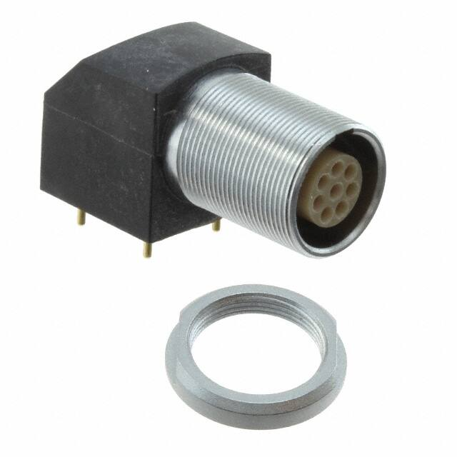


 工商网监
湘ICP备2023018690号
工商网监
湘ICP备2023018690号
