WSB5511M
WSB5511M
3A Schottky Barrier Diode
Http://www.sh-willsemi.com
Features
Low forward voltage
Extremely low thermal resistance
High current capability
SMA (DO-214AC)
Applications
Circuit
Switching circuit
Middle current rectification
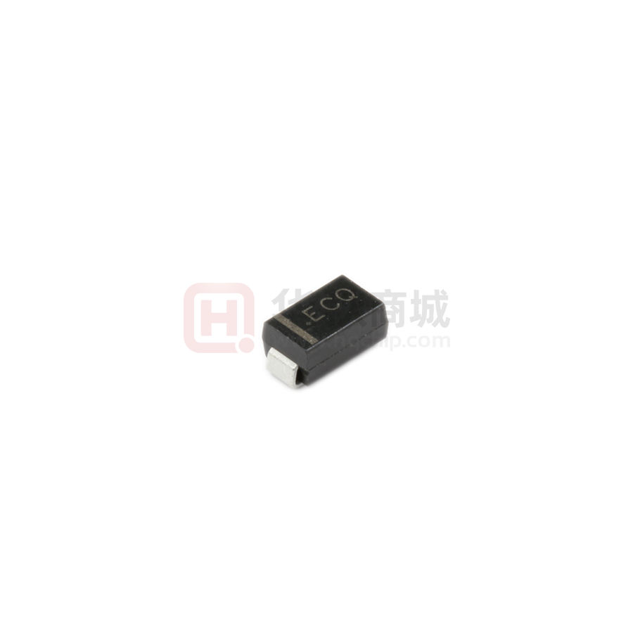
Marking
Absolute maximum ratings
Parameter
Symbol
Value
Unit
VRRM
40
V
Reverse voltage (DC)
VR
40
V
Average rectified forward current (DC)
IO
3.0
A
IFSM
50
A
TJ
-55 ~ 150
O
C
Operating temperature
Topr
-55 ~ 150
O
C
Storage temperature
Tstg
-55 ~ 150
O
C
Reverse voltage (repetitive peak)
Forward Peak Surge Current (1)
Junction temperature
Electronics characteristics (TA=25oC)
Parameter
Symbol
Condition
VF
Reverse current
Junction capacitance
Forward voltage
(2)
Thermal resistance
Min.
Typ.
Max.
Unit
IF=3.0A
0.50
V
IR
VR=40V
0.5
mA
CJ
VR=4V, F=1MHz
220
pF
Rθ(J-L)
Junction to Lead (Fig.2)
17
K/W
Order Informations
Device
WSB5511M-2/TR
Package
Marking
SMA (DO-214AC)
.EC*
(3)
Shipping
5000/Reel&Tape
Note1: Pulse width=8.3ms, single pulse;
Note2: Single Pulse, test Tp=380us;
Note3: * =Month code (A~Z); .EC =Device code;
Will Semiconductor Ltd.
1
Jul, 2019 - Rev. 1.6
�WSB5511M
Typical characteristics (Ta=25oC, unless otherwise noted)
100000
o
o
o
+85 C
o
o
0.1
o
o
+65 C
+25 C
o
0C
0.01
1000
Reverse Current(uA)
+125 C
+85 C
100
o
0C
0.1
o
0.01
1E-3
0.2
o
+25 C
1
o
1E-3
0.0
o
+65 C
10
-50 C
0.4
0.6
-50 C
5
10
15
Fig.1 Forward voltage vs. Forward current
25
30
35
40
Fig.2 Reverse current vs. Reverse voltage
4
1000
800
Cj(pF)
3
2
1
0
20
Reverse Voltage(V)
Forward Voltage(V)
Average Forward Current(A)
Forward Current(A)
1
+125 C
10000
+150 C
600
400
200
0
25
50
75
100
125
0
150
5
10
15
20
25
Reverse Voltage(V)
o
Lead temperature( C)
Fig.3 Maximum Forward Current Derating Curve
Will Semiconductor Ltd.
0
Fig.4 Junction capacitance vs. Reverse voltage
2
Jul, 2019 - Rev. 1.6
�WSB5511M
Package outline dimensions
SMA
Dimensions in millimeters
Symbol
A
Min.
Max.
1.90
2.50
A1
0.203 MAX
D
3.90
4.70
D1
4.75
5.35
E
2.40
2.85
c
0.10
0.31
b
1.27
1.95
L
0.76
1.55
Will Semiconductor Ltd.
3
Jul, 2019 - Rev. 1.6
�WSB5511M
TAPE AND REEL INFORMATION
Reel Dimensions
RD
Reel Dimensions
Tape Dimensions
W
P1
Quadrant Assignments For PIN1 Orientation In Tape
Q1
Q2
Q1
Q2
Q3
Q4
Q3
Q4
RD
Reel Dimension
W
Overall width of the carrier tape
P1
Pitch between successive cavity centers
Pin1
Pin1 Quadrant
Will Semiconductor Ltd.
User Direction of Feed
7inch
13inch
1 8mm
12mm
16mm
2mm
4mm
8mm
Q1
Q2
Q3
4
Q4
Jul, 2019 - Rev. 1.6
�WSB5511M
制
修
订
记
修订页次
录
文件版本
制修日期
修订人
变更内容
Rev.1.0
2013/5/21
建立文档
Rev.1.1
2013/7/24
修改 IF=3A
Rev.1.2
2013/8/28
修改 VF 和 IR 曲线,Marking
Rev.1.3
2013/10/08
修改 VF 与 IR,Cj 曲线
Rev.1.4
2014/01/21
衷世雄
添加 125 度曲线
Rev.1.5
2014/03/17
衷世雄
更换 wafer,相关信息更新
批准
审核
编制
衷世雄
日期
日期
日期
20140527
各部门会签
应用部
Will Semiconductor Ltd.
封装部
市场部
5
生产管理部
Jul, 2019 - Rev. 1.6
�
很抱歉,暂时无法提供与“WSB5511M-2/TR”相匹配的价格&库存,您可以联系我们找货
免费人工找货- 国内价格
- 5+0.40765
- 20+0.37169
- 100+0.33572
- 500+0.29975
- 1000+0.28296
- 2000+0.27097


 工商网监
湘ICP备2023018690号
工商网监
湘ICP备2023018690号
