ESD Protection Diode
PDCSD15CW
Description
Features
The PDCSD15CW is designed to replace multilayer varistors
(MLVs) in portable applications such as cell phones,
notebook computers and PDA’s, using monolithic silicon
technology to provide fast response time and ultra low ESD
clamping voltage, making this device an ideal solution for
protecting sensitive semiconductor components from
damage. The PDCSD15CW complies with the IEC 61000-42 (ESD) with ±30kV air and ±30kV contact discharge. The
PDCSD15CW is assembled into a lead-free SOD-323
package and will protect one bidirectional line. These
devices will fit on the same PCB pad area as an 0805 MLV
device.
250W peak pulse power (8/20μs)
Protects one data or power line
Ultra low leakage:nA level
Operating voltage:15V
Ultra low clamping voltage
2-pin leadless package
Complies with following standards:
– IEC 61000-4-2 (ESD) immunity test Air
discharge: ±30kV
Contact discharge: ±30kV
– IEC61000-4-5 (Lightning) 10A (8/20μs)
RoHS Compliant
Mechanical Characteristics
Applications
Package: SOD-323
Lead Finish: Matte Tin
Case Material: “Green” Molding Compound.
Moisture Sensitivity: Level 3 per J-STD-020
Terminal Connections: See Diagram Below
Marking Information: See Below
Dimensions and Pin Configuration
Marking Information
Cellular Handsets and Accessories
Personal Digital Assistants
Notebooks and Handhelds
Portable Instrumentation
Peripherals
Pagers Peripherals
Desktop and Servers
2J
2J =Device Marking Code
Circuit and Pin Schematic
Ordering Information
Part Number
Marking
Packaging
Reel Size
PDCSD15CW
2J
3000/Tape & Reel
7 inch
www.pdwsemi.com
1 -4
© 2022 PDW, Inc.
Specifications are subject to change without notice.
Revised: 2022/04/08
�ESD Protection Diode
PDCSD15CW
Absolute Maximum Ratings (TA=25°C unless otherwise specified)
Parameter
Symbol
Value
Unit
Peak Pulse Power (8/20µs)
Ppk
250
W
Peak Pulse Current (8/20µs)
Ipp
10
A
ESD per IEC 61000−4−2 (Air)
±30
VESD
ESD per IEC 61000−4−2 (Contact)
Operating Temperature Range
Storage Temperature Range
±30
kV
TJ
−55 to +125
°C
Tstg
−55 to +150
°C
Electrical Characteristics (TA=25°C unless otherwise specified)
Parameter
Reverse Working Voltage
Breakdown Voltage
Symbol
Min
Typ
VRWM
VBR
Max
Unit
15
V
16.5
Test Condition
V
IT = 1mA
Reverse Leakage Current
IR
0.5
µA
VRWM = 15V
Clamping Voltage
VC
20
V
IPP = 1A (8 x 20µs pulse)
Clamping Voltage
VC
25
V
IPP = 10A (8 x 20µs pulse)
Junction Capacitance
CJ
pF
VR = 0V, f = 1MHz
www.pdwsemi.com
17
2 -4
© 2022 PDW, Inc.
Specifications are subject to change without notice.
Revised: 2022/04/08
�ESD Protection Diode
PDCSD15CW
Typical Performance Characteristics (TA=25℃ unless otherwise Specified)
Junction Capacitance vs. Reverse Voltage
Peak Pulse Power vs. Pulse Time
Power Derating Curve
Clamping Voltage vs. Peak Pulse Current
ESD Clamping Voltage
8 kV Contact per IEC61000−4−2
8 X 20μs Pulse Waveform
www.pdwsemi.com
3 -4
© 2022 PDW, Inc.
Specifications are subject to change without notice.
Revised: 2022/04/08
�ESD Protection Diode
PDCSD15CW
SOD-323 Package Outline Drawing
A
DIMENSIO
MILLIMETERS
INCHES
MIN
MAX
MIN
MAX
1.50
1.80
0.060
0.071
SYM
B
1.20
1.40
0.045
0.054
C
2.30
2.70
0.090
0.107
D
-
1.10
-
0.043
E
0.30
0.40
0.012
0.016
F
0.10
0.25
0.004
0.010
H
-
0.10
-
0.004
Suggested Land Pattern
SYM
www.pdwsemi.com
4 -4
DIMENSIONS
MILLIMETERS
INCHES
A
3.15
0.120
B
0.80
0.031
C
0.80
0.031
© 2022 PDW, Inc.
Specifications are subject to change without notice.
Revised: 2022/04/08
�
很抱歉,暂时无法提供与“PDCSD15CW”相匹配的价格&库存,您可以联系我们找货
免费人工找货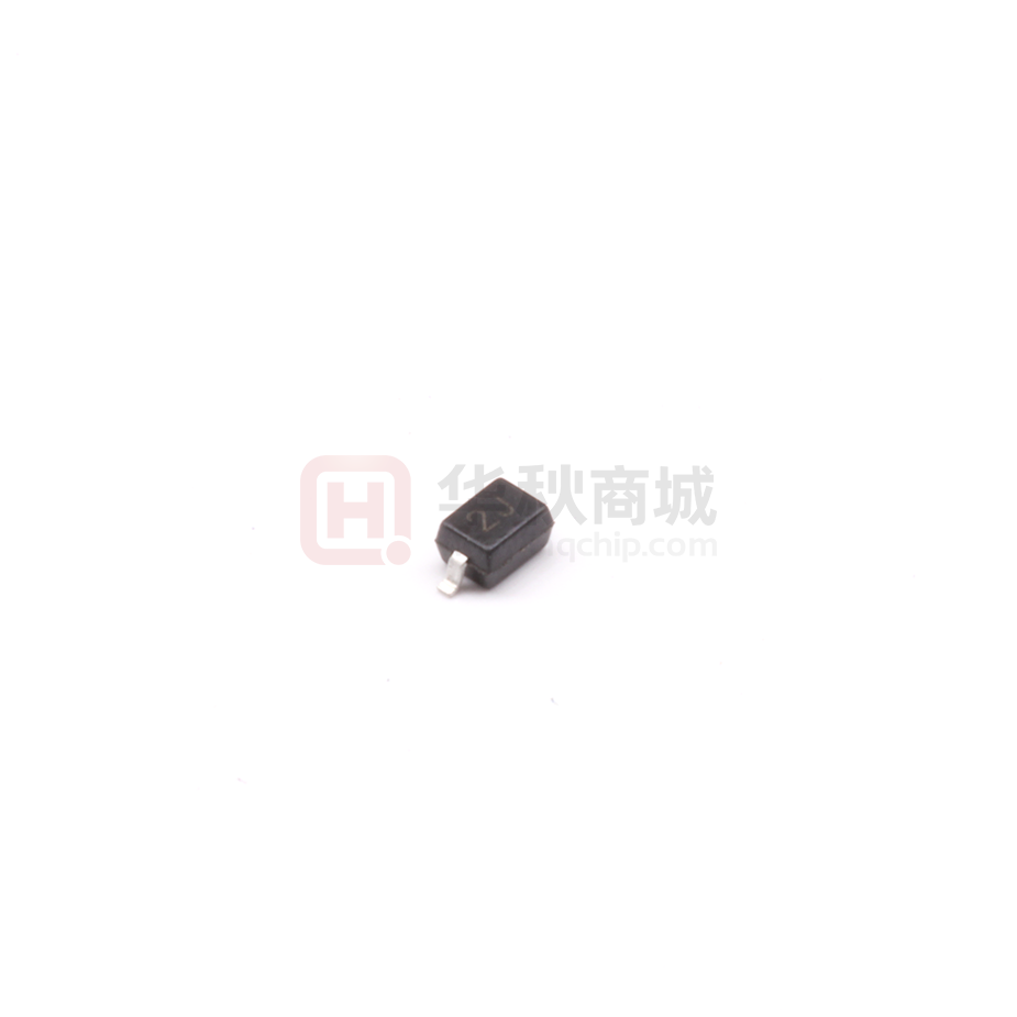


 工商网监
湘ICP备2023018690号
工商网监
湘ICP备2023018690号
