NO.
FUZETEC TECHNOLOGY CO., LTD.
PQ19-01ER
Product Specification and Approval Sheet Version A1
Page
1/4
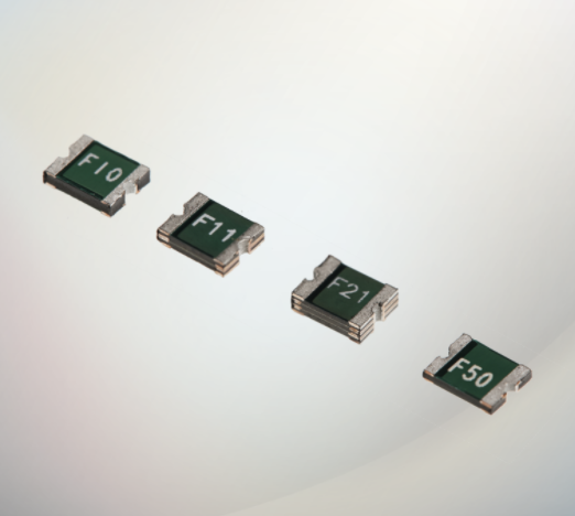
Surface Mountable PTC Resettable Fuse: FSMD1210 Series
1. Summary
(a) RoHS Compliant & Halogen Free
(b) Applications: All high-density boards
(c) Product Features: Small surface mountable, Solid state, Faster time to trip than
standard SMD devices, Lower resistance than standard SMD devices
(d) Operation Current: 0.05A~2.00A
(e) Maximum Voltage: 6V~60VDC
(f) Temperature Range : -40℃ to 85℃
2. Agency Recognition
UL :
C-UL:
TÜ V:
File No. E211981
File No. E211981
File No. R50090556
3. Electrical Characteristics (23℃)
Part
Hold
Trip
Rated
Max
Typical
Max Time to Trip
Current
Current
Voltage
Current
Power
Current
Time
RMIN
R1MAX
IH, A
IT, A
VMAX, VDC
IMAX, A
Pd, W
A
Sec
Ohms
Ohms
0.05
0.10
0.20
0.35
0.50
0.75
0.75
1.10
1.10
1.50
1.75
2.00
0.15
0.25
0.40
0.70
1.00
1.50
1.50
2.20
2.20
3.00
4.00
4.00
60
60
30
16
16
8
24
8
16
6
6
6
100
100
100
100
100
100
100
100
100
100
100
100
0.60
0.60
0.60
0.60
0.60
0.60
0.60
0.80
0.80
0.80
0.80
0.80
0.25
0.50
8.00
8.00
8.00
8.00
8.00
8.00
8.00
8.00
8.00
8.00
1.50
1.50
0.02
0.20
0.10
0.10
0.10
0.30
0.30
0.50
0.60
1.00
3.600
1.600
0.800
0.320
0.250
0.130
0.130
0.060
0.060
0.040
0.020
0.015
50.000
15.000
5.000
1.300
0.900
0.400
0.400
0.210
0.210
0.110
0.080
0.070
Number
FSMD005-1210-R
FSMD010-1210-R
FSMD020-1210-R
FSMD035-1210-R
FSMD050-1210-R
FSMD075-1210-R
FSMD075-24-1210R
FSMD110-1210R
FSMD110-16-1210R
FSMD150-1210R
FSMD175-1210R
FSMD200-1210R
Resistance
IH=Hold current-maximum current at which the device will not trip at 23℃still air.
IT=Trip current-minimum current at which the device will always trip at 23℃ still air.
V MAX=Maximum voltage device can withstand without damage at it rated current.(I MAX)
I MAX= Maximum fault current device can withstand without damage at rated voltage (V MAX).
Pd=Typical power dissipated-type amount of power dissipated by the device when in the tripped state in 23℃ still air environment.
RMIN=Minimum device resistance at 23℃ prior to tripping.
R1MAX=Maximum device resistance at 23℃ measured 1 hour after tripping or reflow soldering of 260℃ for 20 seconds.
Termination pad characteristics
Termination pad materials: Pure Tin
NOTE : Specification subject to change without notice.
2015/12/16
�NO.
FUZETEC TECHNOLOGY CO., LTD.
PQ19-01ER
Product Specification and Approval Sheet Version A1
Page
2/4
4. FSMD Product Dimensions (Millimeters)
Part
Number
FSMD005-1210-R
FSMD010-1210-R
FSMD020-1210-R
FSMD035-1210-R
FSMD050-1210-R
FSMD075-1210-R
FSMD075-24-1210R
FSMD110-1210R
FSMD110-16-1210R
FSMD150-1210R
FSMD175-1210R
FSMD200-1210R
A
B
C
D
E
Min
Max
Min
Max
Min
Max
Min
Max
Min
Max
3.00
3.00
3.00
3.00
3.00
3.00
3.00
3.00
3.00
3.00
3.00
3.00
3.43
3.43
3.43
3.43
3.43
3.43
3.43
3.43
3.43
3.43
3.43
3.43
2.35
2.35
2.35
2.35
2.35
2.35
2.35
2.35
2.35
2.35
2.35
2.35
2.80
2.80
2.80
2.80
2.80
2.80
2.80
2.80
2.80
2.80
2.80
2.80
0.60
0.60
0.40
0.40
0.30
0.30
0.80
0.60
0.60
0.50
0.80
0.80
1.15
1.15
0.85
0.80
0.75
0.70
1.20
1.00
1.00
0.90
1.40
1.40
0.25
0.25
0.25
0.25
0.25
0.25
0.25
0.25
0.25
0.25
0.25
0.25
0.75
0.75
0.75
0.75
0.75
0.75
0.75
0.75
0.75
0.75
0.75
0.75
0.10
0.10
0.10
0.10
0.10
0.10
0.10
0.10
0.10
0.10
0.10
0.10
0.45
0.45
0.45
0.45
0.45
0.45
0.45
0.45
0.45
0.45
0.45
0.45
5. Thermal Derating Curve
FSMD1210 Series
Percent of Rated Hold and Trip Current
200%
150%
100%
50%
0%
-40
-20
0
20
40
60
80
Ambient Temperature (℃)
NOTE : Specification subject to change without notice.
2015/12/16
�NO.
FUZETEC TECHNOLOGY CO., LTD.
PQ19-01ER
Product Specification and Approval Sheet Version A1
Page
3/4
6. Typical Time-To-Trip at 23℃
B
C
D
E
F G
H
IJ
100
10
A
Time to Trip (S)
A =FSMD005-1210 -R
B =FSMD010-1210 -R
C =FSMD020-1210 -R
D =FSMD035-1210 -R
E =FSMD050-1210 -R
F =FSMD075-1210 -R
/ 075-24-1210R
G =FSMD110-1210R
/ 110-16-1210R
H =FSMD150-1210R
I =FSMD175-1210R
J =FSMD200-1210R
1
0.1
0.01
0.001
0.1
1
10
100
Fault Current (A)
7. Material Specification
Terminal pad material: Pure Tin
Soldering characteristics: Meets EIA specification RS 186-9E, ANSI/J-std-002 Category 3
8. Part Numbering and Marking System
Part Numbering System
F S M D □ □ □ – □ □ – 1210 R
Part Marking System
F75
F
□ □
Part Identification
Voltage Rating
Current Rating
Example
F75
F
Example
Fuzetec Logo
F
□ □
□
Part Identification
Fuzetec Logo
Warning: -Operation beyond the specified maximum ratings or improper use may result in damage and possible
甲、
electrical arcing and/or flame.
-PPTC device are intended for occasional overcurrent protection. Application for repeated overcurrent
condition and/or prolonged trip are not anticipated.
-Avoid contact of PPTC device with chemical solvent. Prolonged contact will damage the device
performance.
NOTE : Specification subject to change without notice.
2015/12/16
�FUZETEC TECHNOLOGY CO., LTD.
NO.
PQ19-01ER
Product Specification and Approval Sheet Version A1
Page
4/4
9. Pad Layouts、Solder Reflow and Rework Recommendations
The dimension in the table below provide the recommended pad layout for each FSMD1210 device
Pad dimensions (millimeters)
A
B
Device
Nominal
Nominal
All 1210 Series
2.00
1.00
C
Nominal
2.80
Solder reflow
※ Due to “Lead Free” nature, Temperature and
Profile Feature
Average Ramp-Up Rate (Tsmax to Tp)
Preheat :
Temperature Min (Tsmin)
Temperature Max (Tsmax)
Time (tsmin to tsmax)
Pb-Free Assembly
3 ℃/second max.
Dwelling time for the soldering zone is higher
than those for Regular. This may cause
damage to other components.
150 ℃
200 ℃
60-180 seconds
Time maintained above:
Temperature(TL)
217 ℃
Time (tL)
60-150 seconds
Peak/Classification Temperature(Tp) : 260 ℃
Time within 5℃ of actual Peak :
20-40 seconds
Temperature (tp)
Ramp-Down Rate :
6 ℃/second max.
8 minutes max.
Time 25 ℃ to Peak Temperature :
Note 1: All temperatures refer to of the package,
measured on the package body surface.
1. Recommended max past thickness > 0.25mm.
2. Devices can be cleaned using standard
methods and aqueous solvent.
3. Rework use standard industry practices.
4. Storage Envorinment : < 30℃ / 60%RH
Caution:
1. If reflow temperatures exceed the
recommended profile, devices may not meet
the performance requirements.
2. Devices are not designed to be wave soldered
to the bottom side of the board.
Reflow Profile
NOTE : Specification subject to change without notice.
2015/12/16
�
很抱歉,暂时无法提供与“FSMD050-1210-R”相匹配的价格&库存,您可以联系我们找货
免费人工找货- 国内价格
- 1+0.27301
- 30+0.26326
- 100+0.25351
- 500+0.23400
- 1000+0.22425
- 2000+0.21840


 工商网监
湘ICP备2023018690号
工商网监
湘ICP备2023018690号
