RuiMeng
MS41929
Lens Driver IC for camcorder and securitycamera
Overview
MS41929 is a lens motor driver IC for camcorder and securitycamera featuring the functions of Iris control.
Voltage drive system and several torque ripple correction
techniques enable super- low noise microstep drive.
MS41929 integrated a DC motor driver featuring Infrared
Rejector driver
MS41929 can use 27MHz passive crystal instead
Of oscillator.
Features
Voltage drive system 256-step microstep drivers (2 systems)
H-bridge max current 0.5A
Applications
Motor control by 4-line serial data communication
Camcorder
2 systems of open-drain for driving LED
Security-camera
Infrared Rejector DC motor driver, max current 0.5A
passive crystal
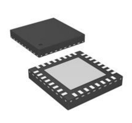
QFN32 package
Package
Part Number
Package
Marking
MS41929
QFN32(0505X0.75-0.5)
MS41929
VERSION:1.2
2015.08.10
Hang zhou Ruimeng Technology Co.,LTD
Http://www.relmon.com
-1-
�RuiMeng
MS41929
Contents
Block Diagram………………………………………………………………………………………..…3
Absolute Maximum Ratings …………………………………………………………………………3
Electrical Characteristics…………………………………………………………………………..…5
Pin Diagram……………………………..……………………………………………………………....9
Pin Descriptions……………………………………………………………………………………….10
Function description …………………………………………………………………………………11
a)Serial Interface…………………………………………………………………………………….11
b)Register detail description……………………………………………………………………...15
c) Micro Stepping Motor Driver …………………..……………………………………………...16
d) Test signals………………………………………………………………………………….……27
e) LED Driver……………………………………………………..……………………………….…30
f) Reset/Protect circuit………………………………………..……………………………………31
g) Infrared Rejector……………………………………….…………………………………….…..32
h) application note……………………………………….…………………………………..……..33
Application Circuit Example………………………………………………………………………..33
Package information………………………………………………………………..………………..34
VERSION:1.2
2015.08.10
Hang zhou Ruimeng Technology Co.,LTD
Http://www.relmon.com
-2-
�RuiMeng
MS41929
Block Diagram
Absolute Maximum Ratings
(Note) Absolute maximum ratings are limit values which do not result in damages to this IC, and IC operation is not guaranteed at
these limit values.
Parameter
Symbol
Rating
Unit
Notes
DVDD
-0.3~+4.0
V
*1
MVCCx ,VDD5
-0.3~+6.0
V
*1
PD
141.1
mW
*2
Operating ambient temperature
Topr
-20~+85
℃
*3
Storage temperature
Tstg
-55~+125
℃
*3
Controller supply voltage
Supply voltage for motor controller
Power dissipation
VERSION:1.2
2015.08.10
Hang zhou Ruimeng Technology Co.,LTD
Http://www.relmon.com
-3-
�RuiMeng
MS41929
Motor driver 1 (focus, zoom) H bridge
drive current
IM1(CD)
±0.5
A/ch
─
Instantaneous H bridge drive current
IM(pluse)
±0.6
A/ch
─
Vin
-0.3~(DVDD + 0.3)
V
*4
HBM
±3k
V
-
Digital input voltage
ESD
(Notes)
*1 : The values under the condition not exceeding the above absolute maximum ratings and the power dissipation.
*2 : The power dissipation shown is the value at Ta = 85°C for the independent (unmounted) IC package without a heat sink.
When using this IC, refer to the PD-Ta diagram of the package standard and design the heat radiation with sufficient margin so
that the
allowable value might not be exceeded based on the conditions of power supply voltage, load, and ambient temperature.
*3 : Except for the power dissipation, operating ambient temperature, and storage temperature, all ratings are for Ta = 25°C.
*4 : (DVDD + 0.3 ) V must not be exceeded 4.0 V.
Operating Supply Voltage Range
Parameter
Symbol
Range
Min
Typ
Max
DVDD
2.7
3.1
3.6
MVCCx
3.0
4.8
5.5
Supply voltage range
Unit
Notes
V
*1
(Note)
*1 : The values under the condition not exceeding the above absolute maximum ratings and the power dissipation.
Allowable Current and Voltage Range
(Notes)
Allowable current and voltage ranges are limit ranges which do not result in damages to this IC, and IC operation is not
guaranteed within these limit ranges.
Voltage values, unless otherwise specified, are with respect to GND.
GND is voltage for GNDD, GND5, MGNDA, and MGNDB. GND = GNDD = GND5 = MGNDA = MGNDB
VCC3V is voltage for DVDD.VCC3V = DVDD
Do not apply external currents or voltages to any pin not specifically mentioned.
For the circuit currents, "+" denotes current flowing into the IC, and "–" denotes current flowing out of the IC.
Pin No
Pin name
Rating
Unit
Notes
24
OSCIN
-0.3~(DVDD + 0.3)
V
*1
23
OSCOUT
-0.3~(DVDD + 0.3)
V
*1
27
CS
-0.3~(DVDD + 0.3)
V
*1
26
SCK
-0.3~(DVDD + 0.3)
V
*1
29
SIN
-0.3~(DVDD + 0.3)
V
*1
30
VD_FZ
-0.3~(DVDD + 0.3)
V
*1
VERSION:1.2
2015.08.10
Hang zhou Ruimeng Technology Co.,LTD
Http://www.relmon.com
-4-
�RuiMeng
MS41929
1
RSTB
-0.3~(DVDD + 0.3)
V
*1
8
OUTD2
±0.5
A
─
10
OUTD1
±0.5
A
─
11
OUTC2
±0.5
A
─
13
OUTC1
±0.5
A
─
14
OUTB2
±0.5
A
─
16
OUTB1
±0.5
A
─
17
OUTA2
±0.5
A
─
19
OUTA1
±0.5
A
─
7
OUTE1
±0.5
A
─
5
OUTE2
±0.5
A
─
20
LED1
30
mA
─
21
LED2
30
mA
─
(Note)
*1 : (DVDD3 + 0.3) V must not be exceeded 4.0 V
Electrical Characteristics
(Note)
MVCCx =VDD 5 =4.8 V, DVDD = 3.1 V
Ta = 25°C±2°C unless otherwise specified.
Parameter
Symbol
Conditions
Min
Typ
Max
Unit
IOmdisable
No load, no 27 MHz input
─
0
3.0
μA
Imenable
Output open
─
0.5
1.5
mA
3 V supply current on Reset
Icc3reset
No 27 MHz input
─
0
10.0
μA
3 V supply current on Enable
Icc3enable
Output open
─
3.6
20.0
mA
Supply current on Standby
Iccstandby
─
5.0
10.0
mA
Supply current when FZ is
Enable
ICCps
─
6.0
12.0
mA
Current circuit, Common circuit
MVCC supply current on
Reset
MVCC supply current on
Enable
RSTB = High, output open,
27 MHz input,
Total current
RSTB = High, output open,
27 MHz input, FZ = Enable,
Total current
Digital input / output
High-level input
Vin(H)
RSTB
Low-level input
Vin(L)
RSTB
SOUT High-level output
VERSION:1.2
Vout(H):
SDATA
[SOUT] 1mA(Source)
2015.08.10
0.54×
DVDD
-0.3
DVDD
-0.5
─
─
─
DVDD
+0.3
0.2×
DVDD
─
V
V
V
Hang zhou Ruimeng Technology Co.,LTD
Http://www.relmon.com
-5-
�RuiMeng
SOUT High-level output
PLS1 to 2 High-level output
PLS1 to 2 Low-level output
MS41929
Vout(L):
SDATA
[SOUT] 1mA (Sink)
Vout(H):
─
MUX
Vout(L):
MUX
─
0.9×
DVDD
─
0.5
V
─
─
V
─
─
─
0.1×
DVDD
V
Input pull-down resistance
Rpullret
RSTB
50
100
200
kΩ
Parameter
Symbol
Conditions
Min
Typ
Max
Unit
H bridge ON resistance
RonFZ
IM = 100mA
0.6
0.8
1.4
Ω
H bridge leak current
IleakFZ
─
─
─
0.8
μA
Output ON resistance
RonLED
IM = 20mA,5Vcell
1.2
1.6
2.6
Ω
Output leak current
IleakLED
─
─
─
0.8
μA
Motor driver 1 (focus, zoom)
LED driver
Infrared Rejector driver(DRIVER E ) VDD5=5V,RL=20Ω,T=25℃
Output ON resistance
Roncut
IoutE=300mA
H bridge leak current
IleakE
─
Output enable time
T7
Output disable time
1.1
─
─
Ω
0.8
μA
RL=20Ω
300
ns
T8
RL=20Ω
300
ns
T9
RL=20Ω
160
ns
T10
RL=20Ω
160
ns
Output rise time
T11
RL=20Ω
30
188
ns
Output fall time
T12
RL=20Ω
30
188
ns
T13
SPI control,RL=20Ω
delay time, INx high to OUTx
high
Delay time, INx low to OUTx
low
Delay time, SPI IN to OUTx
change
VERSION:1.2
25*TSC
s
K
2015.08.10
Hang zhou Ruimeng Technology Co.,LTD
Http://www.relmon.com
-6-
�RuiMeng
MS41929
Serial port input
Serial clock
Sclock
─
1
─
5
MHz
SCK low time
Ts1
─
100
─
─
ns
SCK high time
Ts2
─
100
─
─
ns
CS setup time
Ts3
─
60
─
─
ns
CS hold time
Ts4
─
60
─
─
ns
CS disable high time
Ts5
─
100
─
─
ns
SIN setup time
Ts6
─
50
─
─
ns
SIN hold time
Ts7
─
50
─
─
ns
SOUT delay time
Ts8
─
─
─
60
ns
SOUT hold time
Ts9
─
60
─
─
ns
SOUT Enable-Hi-Z time
Ts10
─
─
─
60
ns
SOUT Hi-Z-Enable time
Ts11
─
─
─
60
ns
Sout C load
Tsc
─
─
─
40
pF
─
1.36
─
V
─
1.02
─
V
100
─
─
μs
─
0.34
─
V
Digtal input/output
High-level
input threshold voltage
Low-level
input threshold voltage
Vin(H)
Vin(L)
SCK,SIN,CS,OSCIN,
VD_FZ
SCK,SIN,CS,OSCIN,
VD_FZ
RSTB signal pulse width
Trst
─
Input hysteresis width
Vhysin
Video sync. signal width
VDw
─
80
─
─
μs
CS signal wait time 1
T(VD-CS)
─
400
─
─
ns
CS signal wait time 2
T(CS-DT1)
─
5
─
─
μs
Pulse start resolution for
pulse 1
PL1wait
OSCIN = 27MHz
─
20.1
─
μs
Pulse resolution for pulse 1
PL1width
OSCIN = 27MHz
─
1.2
─
μs
Pulse start resolution for
pulse 2
PL2wait
OSCIN = 27MHz
─
20.1
─
μs
SCK,SIN,CS,OSCIN,
VD_FZ
Pulse generator
VERSION:1.2
2015.08.10
Hang zhou Ruimeng Technology Co.,LTD
Http://www.relmon.com
-7-
�RuiMeng
MS41929
Thermal shutdown
Thermal shutdown operation
temperature
Thermal shutdown
hysteresis
temperature
Ttsd
─
─
145
─
°C
ΔTtsd
─
─
35
─
°C
3.3 V Reset operation
Vrston
─
─
2.48
─
V
3.3 V Reset hysteresis width
Vrsthys
─
─
0.2
─
V
VrstFZon
─
─
2.42
─
V
VrstFZhys
─
─
0.21
─
V
Supply voltage monitor circuit
VDD5,MVCCx Reset
operation
VDD5,MVCCx Reset
hysteresis width
VERSION:1.2
2015.08.10
Hang zhou Ruimeng Technology Co.,LTD
Http://www.relmon.com
-8-
�RuiMeng
MS41929
Pin diagram
QFN32
VERSION:1.2
2015.08.10
Hang zhou Ruimeng Technology Co.,LTD
Http://www.relmon.com
-9-
�RuiMeng
MS41929
Pin Descriptions
Pin NO.
Pin name
I/O
QFN32
VERSION:1.2
Description
2
IN1
Input
Infrared Rejector logic in1
3
IN2
Input
Infrared Rejector logic in2
5
OUTE2
Output
Infrared Rejector motor out2
4
VDD5
Power
Power for Infrared Rejector
6
GND5
Ground
Groud for Infrared Rejector
7
OUTE1
Output
Infrared Rejector motor out1
8
OUTD2
Output
Motor output D2
9
MVCCB
Power
Power supply for motor B
10
OUTD1
Output
Motor output D1
11
OUTC2
Output
Motor output C2
12
MGNDB
Ground
GND for motor B
13
OUTC1
Output
Motor output C1
14
OUTB2
Output
Motor output B2
15
MVCCA
Power
Power supply for motor A
16
OUTB1
Output
Motor output B1
17
OUTA2
Output
Motor output A2
18
MGNDA
Ground
GND for motor A
19
OUTA1
Output
Motor output A1
20
LED1
Input
Open-drain 1 for driving LED
21
LED2
Input
Open-drain 2 for driving LED
22
GNDD
Ground
23
OSCOUT
Inout
OSC output (cryctal 2)
24
OSCIN
Inout
OSC input (cryctal 1)
25
DVDD
Power
3 V digital power supply
28
SOUT
Output
Serial data output
27
CS
Input
Chip select signal input
26
SCK
Input
Serial clock input
29
SIN
Input
Serial data input
30
VD_FZ
Input
Focus zoom sync. signal input
31
PLS1
Output
Pulse 1 output
32
PLS2
Output
Pulse 2 output
1
RSTB
Input
2015.08.10
Digital GND
Reset signal input
Hang zhou Ruimeng Technology Co.,LTD
Http://www.relmon.com
- 10 -
�RuiMeng
MS41929
Function Description
a)Serial Interface
(Note)
1)CS default value of each cycle (Write / Read mode) starts from Low-level.
2)It is necessary to input the system clock OSCIN at write mode.
VERSION:1.2
2015.08.10
Hang zhou Ruimeng Technology Co.,LTD
Http://www.relmon.com
- 11 -
�RuiMeng
MS41929
Serial Interface Specifications:
Data transfer starts at the rising edge of CS, and stops at the falling edge of CS.
One unit of data is 24 bits. (24 bits of the following format are called a data set in this book.)
Address and data are serially input from SIN pin in synchronization with the data clock SCK at CS = 1.
Data is retrieved at the rising edge of SCK.
Moreover, data is output from SOUT pin at data readout. (Data is output at the rising edge of SCK.)
SOUT outputs Hi-Z at CS = 0, and outputs "0" except data readout at CS = 1.
The control circuit of serial interface is reset at CS = 0.
Date Format:
0
1
2
3
4
5
6
7
A0
A1
A2
A3
A4
A5
C0
C1
8
9
10
11
12
13
14
15
D0
D1
D2
D3
D4
D5
D6
D7
16
17
18
19
20
21
22
23
D8
D9
D10
D11
D12
D13
D14
D15
C0 : Register write / read selection 0 : write mode, 1 : read mode
C1 : Unused
A5 to A0 : Address of register
D15 to D0 : Data written in register
Register Map:
D15
0BH
20H
D14
D13
D12
D11
Reserved
PWMRES[1:
0]
D10
D9
D8
D7
MOD Reser TEST
ESEL ved EN1
PWMMODE[4:0]
TEST
EN2
PHMODAB[5:0]
23H
24H
D2
D1
D0
Reserved
FZTEST[4:0]
PSUMAB[7:0]
INTCTAB[15:0]
PHMODCD[5:0]
28H
DT2B[7:0]
PPWD[7:0]
PPWC[7:0]
MICROCD[1
ENDI BRA CCW
LEDA
:0]
SCD KEC CWC
2AH
VERSION:1.2
D3
PPWA[7:0]
MICROAB[1
ENDI BRA CCW
LEDB
:0]
SAB KEAB CWA
27H
29H
D4
DT2A[7:0]
PPWB[7:0]
25H
D5
DT1[7:0]
21H
22H
D6
PSUMCD[7:0]
INTCTCD[15:0]
2015.08.10
Hang zhou Ruimeng Technology Co.,LTD
Http://www.relmon.com
- 12 -
�RuiMeng
MS41929
2CH
SEL
IN1
IN2
Register List:
Address
0Bh
20h
21h
22h
23h
24h
25h
27h
28h
29h
2Ah
2Ch
Register name / Bit wide
Function
Page
TESTEN1
Test mode enable 1
28
MODESEL_FZ
VD_FZ polarity selection
16
DT1[7:0]
Start point wait time
20
PWMMODE[4:0]
Micro step output PWM frequency
22
PWMRES[1:0]
Micro step output PWM resolution
22
FZTEST[4:0]
PLS1/2 pin output signal selection
28
TESTEN2
Test mode enable 2
28
DT2A[7:0]
α motor start point excitation wait time
21
PHMODAB[5:0]
α motor phase correction
23
PPWA[7:0]
Driver A peak pulse width
23
PPWB[7:0]
Driver B peak pulse width
23
PSUMAB[7:0]
α motor step count number
24
CCWCWAB
α motor rotation direction
24
BRAKEAB
α motor brake
25
ENDISAB
α motor enable/disable control
25
LEDB
LED B output control
31
MICROAB[1:0]
α motor sine wave division number
26
INTCTAB[15:0]
α motor step cycle
26
DT2B[7:0]
β motor start point excitation wait time
21
PHMODCD[5:0]
β motor phase correction
23
PPWC[7:0]
Driver C peak pulse width
23
PPWD[7:0]
Driver D peak pulse width
23
PSUMCD[7:0]
β motor step count number
24
CCWCWCD
β motor rotation direction
24
BRAKECD
β motor brake
25
ENDISCD
β motor enable/disable control
25
LEDA
LED A output control
30
MICROCD[1:0]
β motor sine wave division number
26
INTCTCD[15:0]
β motor step cycle
26
SEL
Infrared Rejector input model selector
32
IN1
Infrared Rejector SPI model input1
32
IN2
Infrared Rejector SPI model input2
32
Note: All the SIF functions containing a data register are formatted at RSTB = 0.
VERSION:1.2
2015.08.10
Hang zhou Ruimeng Technology Co.,LTD
Http://www.relmon.com
- 13 -
�RuiMeng
MS41929
Register Setup Timing:
Address
0Bh
20h
21h
22h
23h
24h
25h
27h
28h
29h
2Ah
Register Name
Setup Timing
TESTEN1
CS
MODESEL_FZ
CS
DT1[7:0]
VD_FZ
PWMMODE[4:0]
DT1
PWMRES[1:0]
DT1
FZTEST[4:0]
CS
TESTEN2
CS
DT2A[7:0]
DT1
PHMODAB[5:0]
DT2A
PPWA[7:0]
DT1
PPWB[7:0]
DT1
PSUMAB[7:0]
DT2A
CCWCWAB
DT2A
BRAKEAB
DT2A
ENDISAB
DT1 or DT2A*
LEDB
CS
MICROAB[1:0]
DT2A
INTCTAB[15:0]
DT2A
DT2B[7:0]
DT1
PHMODCD[5:0]
DT2B
PPWC[7:0]
DT1
PPWD[7:0]
DT1
PSUMCD[7:0]
DT2B
CCWCWCD
DT2B
BRAKECD
DT2B
ENDISCD
DT1 or DT2B*
LEDA
CS
MICROCD[1:0]
DT2B
INTCTCD[15:0]
DT2B
In principle, the setup of registers for micro step should be performed during the interval of start point wait
(Refer to the figure in page 15). The data which is written at timing except the interval of start point wait can be
also received. However, ifthe write operation continues after the reflecting timing such as the end of start point
excitation wait, the setup reflection timing may not be performed at the intended timing (Refer to the following
figure). For example, if the data 1 to 4 which is updated at the end of start point excitation wait are written as the
following figure, data 1 and 2 is updated at the timing a, anddata 3 and 4 is updated at the timing b. Even if the
VERSION:1.2
2015.08.10
Hang zhou Ruimeng Technology Co.,LTD
Http://www.relmon.com
- 14 -
�RuiMeng
MS41929
data is written continuously like this, the update timing may be shifted to 1VD.
Due to the above reason, the setup of registers should be performed during the interval of start point wait in
order to reflectthe updated content certainly.
In this LSI, reflection timing and rotation timing of a stepping motor are based on the rising edge of VD_IS
and
VD_FZ respectively. The polarities of VD_IS and VD_FZ which are used for the internal processing can be
set by thefollowing setup.
b) Register detail description
MODESEL_FZ (VD_FZ polarity selection)
Address
D15
D14
0Bh
D13
D12
D11
Initial value
D10
D9
D8
D7
0
D6
D5
D4
D3
D2
D1
D0
MODE
SEL_F
Z
MODESEL_FZ respectively set the polarities of VD_FZ signals which is input tothis IC.
When setting to "0", the polarity is based on the rising edge of VD_FZ inputted.
When setting to "1", the polarity is based on the falling edge of VD_FZ inputted.
Setup value
VD polarity
0
Non-inverting
1
Inverting
VERSION:1.2
2015.08.10
Hang zhou Ruimeng Technology Co.,LTD
Http://www.relmon.com
- 15 -
�RuiMeng
MS41929
c) Micro Stepping Motor Driver
Block Diagram
This block is a stepping motor driver for focus and zoom, and the following setup can be performed by
serial control.(The following description is for α motor: driver A/B. β motor: driver C/D is the same function as α
motor .)
VERSION:1.2
2015.08.10
Hang zhou Ruimeng Technology Co.,LTD
Http://www.relmon.com
- 16 -
�RuiMeng
MS41929
Main setup parameters
1)
Phase correction : The phase difference between a driver A and a driver B is on the basis of 90 degree,
and can be adjusted from –22.5 degree to +21.8 degree.
2)
・・・PHMODAB[5:0]
Amplitude correction : It is possible to set the load current of driver A/B independently. ・・・PPWA[7:0],
PPWB[7:0]
3)
PWM frequency : PWM driver chopping frequency is set.
・・・PWMMODE[4:0],
PWMRES[1:0]
4)
Quasi-sine wave : Number of divisions can be set to 64, 128 and 256.
5)
Stepping cycle : Motor rotation speed is set. The rotation speed is constant regardless of number of
・・・MICROAB[1:0]
divisions of quasi-sine wave.
・・・INTCTAB[15:0]
Setup Timing for Each Setup
Setup timing and number of times are shown as follows.
Since the setups for address 27h to 2Ah are the same as those of 22h to 25h, the descriptions for address
27h to 2Ah are omitted.
If each setup is set once, the setup is reflected at every VD pulses. Therefore, when the same setup is
performed at two or more VD pulses, it is unnecessary to write at every VD pulse.
DT1[7:0] (Start point wait, Address 20h)
Update timing is set. After hard reset release (Pin 39 RSTB : Low → High), this setup should be performed
before starting to excite and drive a motor.
Since this setup is updated by the start of VD, it is unnecessary to write during the start point wait.
PWMMODE[4:0],PWMRES[1:0] (Micro step output PWM frequency setup,Address 20h)
Micro step output PWM frequency is set. After hard reset release (Pin 39 RSTB : Low to High), this setup
should be performed before starting to excite and drive a motor (DT1 ends).
DT2A[7:0] (Start point excitation wait, Address 22h)
Updated timing is set. After hard reset release (Pin 39 RSTB : Low → High), this setup should be
performed before starting to excite and drive a motor (DT1 ends).
PHMODAB[5:0] (Phase correction, Address 22h)
The correlation phase difference between coil A and B is corrected, and the driving noise is reduced. Since
the amount of suitable phase correction depends on the rotation direction or rotation speed, the change of this
setup should be performed simultaneously with the changes of the rotations direction (CCWCWAB) or rotation
speed (INTCTAB), or it should be performed when a motor does not rotate.
PPWA[7:0],PPWB[7:0] (Peak pulse width, Address 23h)
PWM maximum duty is set. This setup should be performed before starting to excite and drive a motor
(DT1 ends).
PSUMAB[7:0] (Step count number, Address 24h)
The amount of motor rotations in 1 VD interval is set. Every time VD pulse is input, the motor keeps rotating
depending on the amount of rotations. Therefore, set to "0" in order to stop rotation of the motor.
When the amount of rotations which exceeds 1 VD interval is set, the amount of rotations of a part which
VERSION:1.2
2015.08.10
Hang zhou Ruimeng Technology Co.,LTD
Http://www.relmon.com
- 17 -
�RuiMeng
MS41929
exceeds 1 VD interval is cancelled
CCWCWAB (Rotation direction, Address 24h)
Rotation direction is set. This setup should be performed just before switching the rotation direction.
BRAKEAB (Brake setup, Address 24h)
A current is set to 0 by braking. Since it becomes impossible to get the excitation position of a motor by
braking, this setup should not be preformed except for the case of stopping immediately.
ENDISAB (Motor enable/disable setup, Address 24h)
Enable of a motor is set. Since a motor pin is Hi-Z when it is set to "Disable", do not set to "Disable" while a
motor keeps rotating.
LEDA (LED setup, Address 24h)
LED ON/OFF is set. The setup is performed at the falling edge of CS.
(It is understood that it is not related to driving a motor. It is possible to turn ON/OFF independently.)
MICROAB[1:0] (Number of sine wave divisions, Address 24h)
Number of sine wave divisions is set. Even if this setup is changed, the amount of rotations and rotation
speed do not vary.
If only the control which the number of divisions varies depending on the rotation speed is not performed,
the problem dose not occur if it is set once after hard reset release (Pin 39 RSTB : Low → High).
VERSION:1.2
2015.08.10
Hang zhou Ruimeng Technology Co.,LTD
Http://www.relmon.com
- 18 -
�RuiMeng
MS41929
INTCTAB[15:0] (Pulse cycle, Address 25h)
Pulse cycle is set. Rotation speed is determined by this setup.
How to adjust register setting for micro stepping motor driver
In order to control lens, it is required to set motor rotation speed and amount of rotation per VD. Register
settings relating to speed and amount of rotation are:
INTCTxx[15:0]: set time of each step (that is, the rotation speed)
PSUMxx[7:0]: amount of rotation per VD period
When driving the motor continuously for several VD period, it is best to match rotation time (per VD) to VD
period.
Below is a method to calculate INTCTxx[15:0] and PSUMxx[7:0] for smooth motor rotation.
1)
Calculate INTCTxx[15:0] from desired rotation speed.
INTCTxx[15:0] × 768 = OSCIN frequency / rotation frequency
2)
Calculate PSUMxx[7:0] from INTCTxx[15:0]. Round off if the result of PSUMxx[7:0] is not integer.
When the below equation is satisfied, the rotation time is equal to VD period, and smooth rotation is
realized.
INTCTxx[15:0] × PSUMxx[7:0] × 24 = OSCIN frequency / VD frequency
3)
If PSUMxx[7:0] is rounded off, recalculate INTCTxx[15:0] from the equation in 2).
Example) OSCIN frequency = 27 MHz, VD frequency = 60 Hz
Calculate PSUMxx[7:0] and INTCTxx[15:0] to rotate motor at 800 pps (1-2 phase).
800 pps = 100 Hz, so from equation in 1),
INTCTxx[15:0] = 27 MHz / (100 Hz × 768) = 352
Next, calculate PSUMxx[7:0] from equation in 2):
PSUMxx[7:0] = 1/(60 Hz) × 27 MHz / (352 × 24) = 53
Since PSUMxx[7:0] is rounded off, recalculate INTCTxx[15:0] from equation in 2):
INTCTxx[15:0] = 1/(60 Hz) × 27 MHz / (53 × 24) = 354
Refer to pages 24 and 26 for detail of PSUMxx[7:0] and INTCTxx[15:0].
If the value of left-hand side in 2) is smaller than right-hand side, the rotation time will be shorter than VD
period and will cause discontinuous rotation. If left-hand side is smaller, the rotation time that exceeds 1 VD will
be cancelled.
Detail descriptions of register
DT1[7:0] (Start point wait time)
Address
D15
D14
VERSION:1.2
20h
D13
D12
D11
Initial Value
D10
D9
D8
D7
2015.08.10
0Ah
D6
D5
D4
D3
DT1[7:0]
D2
D1
D0
Hang zhou Ruimeng Technology Co.,LTD
Http://www.relmon.com
- 19 -
�RuiMeng
MS41929
DT1[7:0] sets the delay time (start point wait time) until the data written in the serial data communication
sends to the output.
It becomes possible to excite a motor after a start point wait switches "1" to "0". The start point wait starts
to count after the rising edge of video sync signal (VD_FZ).
Since start point wait time is the trigger required for data acquisition, be sure to set to other than "0". When
the value of register is "0", the data cannot be updated.
Refer to page 19 for the relationship of VD_FZ and start point wait time.
DT1
Start point wait
0
Prohibition
1
303.4μs
255
77.4ms
n
n×8192/27MHz
DT2A[7:0]( Start point excitation wait α motor)
Address
22h
03h
Initial Value
D15 D14 D13 D12 D11 D10
D9
D8
D7
D6
D5
D4 D3
DT2A[7:0]
D2
D1
D0
D4 D3
DT2B[7:0]
D2
D1
D0
DT2B[7:0]( Start point excitation wait β motor)
Address
27h
Initial Value
D15 D14 D13 D12 D11 D10
D9
D8
D7
03h
D6
D5
DT2A[7:0] and DT2B[7:0] set the delay time (start point excitation wait) until α motor and β motor start
rotation.
Motor rotation starts after start point excitation wait switches "1" to "0". The start point excitation wait starts
to count after the falling edge of start point wait.
Since the falling edge is the trigger pulse which is required for data acquisition, be sure to input the data of
other than "0". When the value of register is "0", the data cannot be updated.
Refer to page 19 for the relationship of VD_FZ and start point excitation wait time.
DT1
Start point excitation wait
0
Prohibition
1
303.4μs
255
77.4ms
n
n×8192/27MHz
PWMMODE[4:0] (Micro step output PWM frequency)
VERSION:1.2
2015.08.10
Hang zhou Ruimeng Technology Co.,LTD
Http://www.relmon.com
- 20 -
�RuiMeng
Address
MS41929
20h
Initial Value
D15 D14 D13 D12 D11 D10 D9 D8
PWMMODE[4:0]
D7
1Ch
D6
D5
D4
D3
D2
D1
D0
D4
D3
D2
D1
D0
PWMRES[1:0] (Micro step output PWM frequency resolution)
Address
20h
Initial Value
D15 D14 D13 D12 D11 D10
PWMRES
D9
D8
D7
1
D6
D5
PWMMODE[4:0] sets the frequency division value of system clock, OSCIN, which is used as the standard of
PWM signal for micro step output. PWMMODE[4:0] can set in the range from 1 to 31. PWM frequency at
PWMMODE = 0 is the same as that at PWMMODE = 1.
PWMRES[1:0] sets the resolution of frequency division value set by PWMMODE[4:0].
PWM frequency is calculated by the following formula.
3
PWM frequency = OSCIN frequency / ((PWMMODE×2 ) × 2PWMRES)
Table for the specific PWM frequency set by PWMMODE[4:0] and PWMRES[1:0] at OSCIN = 27 MHz..
PWMMODE
PWMRES(kHZ)
0
1
2
1
3375.0
1687.5
843.8
2
1687.5
843.8
3
1125.0
4
PWMMODE
PWMRES(kHZ)
0
1
2
17
198.5
99.3
49.6
421.9
18
187.5
93.8
46.9
526.5
281.3
19
177.6
88.8
44.4
843.8
421.9
210.9
20
168.8
84.4
42.2
5
675.0
337.5
168.8
21
160.7
80.4
40.2
6
526.5
281.3
140.6
22
153.4
76.7
38.4
7
482.1
241.1
120.5
23
146.7
73.4
36.7
8
421.9
210.9
105.5
24
140.6
70.3
35.2
9
375.0
187.5
93.8
25
135.0
67.5
33.8
10
337.5
168.8
84.4
26
129.8
64.9
32.5
11
306.8
153.4
76.7
27
125.0
62.5
31.3
12
281.3
140.6
70.3
28
120.5
60.3
30.1
13
259.6
129.8
64.9
29
116.4
58.2
29.1
14
241.1
120.5
60.3
30
112.5
56.3
28.1
15
225.0
112.5
56.3
31
108.9
54.4
27.2
16
210.9
105.5
52.7
VERSION:1.2
2015.08.10
Hang zhou Ruimeng Technology Co.,LTD
Http://www.relmon.com
- 21 -
�RuiMeng
MS41929
PHMODAB[5:0] (Phase correction α motor)
Address
22h
Initial Value
D15 D14 D13 D12 D11 D10 D9
PHMODAB[5:0]
D8
D7
0
D6
D5
D4
D3
D2
D1
D0
D4
D3
D2
D1
D0
PHMODCD[5:0] (Phase correction β motor)
27h
Address
Initial Value
D15 D14 D13 D12 D11 D10 D9
PHMODCD[5:0]
D8
D7
0
D6
D5
Current phase differences of α motor and β motor shifts from 90 degree by PHMODAB[5:0] and
PHMODCD[5:0]
respectively. Setup resolution is 0.7 degree, and data is set in two's complement.
PHMODAB
Amount of phase
correction
000000
±0°
000001
+0.7°
011111
+21.80°
100000
-22.50°
111111
-0.7°
Resolution
360°/512 = 0.70°
Stepping motor is configured so that phase difference between coils becomes 90 degree. However, the
phase difference may shift from 90 degree due to the variation of a motor.
Therefore, even if phase difference in current waveform is exactly 90 degree, driving noise may occur due
to the occurrence of rotation torque ripple.
This setup is for reducing the torque ripple which is occurred by the variation of a motor.
PPWA[7:0] (Driver A peak pulse width)
PPWB[7:0] (Driver B peak pulse width)
Address
23h
D15 D14 D13 D12 D11 D10
PPWB[7:0]
Initial Value
D9
D8
D7
0,0
D6
D5
D4 D3 D2
PPWA[7:0]
D1
D0
D4 D3 D2
PPWC[7:0]
D1
D0
PPWC[7:0] (Driver C peak pulse width))
PPWD[7:0] (Driver D peak pulse width)
Address
28h
D15 D14 D13 D12 D11 D10
PPWD[7:0]
VERSION:1.2
Initial Value
D9
D8
D7
2015.08.10
0,0
D6
D5
Hang zhou Ruimeng Technology Co.,LTD
Http://www.relmon.com
- 22 -
�RuiMeng
MS41929
PPWA[7:0] to PPWD[7:0] set the maximum duty of PWM at the position which the currents in driver A to D
are peak value respectively. The maximum duty is calculated by the following formula.
Driver X Maximum duty = PPWx / (PWMMODE × 8)
When PPWx = 0 is set, coil current becomes 0.
when the duty exceeding 100% is set,Since the duty does not certainly exceed 100% at PWM operation in
this case, the peak point of sine wave (current waveform) becomes flat.
(Example) When PPWA[7:0] = 200, PWMMODE[4:0] = 28 is set, maximum duty of driver A will be
200 / (28 × 8) = 0.89
PSUMAB[7:0] (α motor step count number)
Address
24h
0
Initial Value
D15 D14 D13 D12 D11 D10
D9
D8
D7
D6
D5
D4 D3 D2
PSUMAB[7:0]
D1
D0
D4 D3 D2
PSUMCD[7:0]
D1
D0
PSUMCD[7:0] (β motor step count number)
Address
29h
0
Initial Value
D15 D14 D13 D12 D11 D10
D9
D8
D7
D6
D5
PSUMAB[7:0] and PSUMCD[7:0] set the number of step counts of α motor and β motor respectively.
Since the number of setup step counts is converted to 256-step inside, the amount of rotation becomes the
same regardless of the number of divisions.
To stop the rotation of a motor, set PSUMxx[7:0] = 0.
Number of steps
Setting
64-step
128-step
256-step
conversion
conversion
conversion
0
0
0
0
1
2
4
8
255
510
1020
2040
n
2n
4n
8n
value
If maximum duty is set to other than "0" at PSUMxx[7:0] = 0, the position is held in the state of excitation.
If a motor can hold the position by cogging torque without motor current, the position is held even if the
maximum duty is set to 0.
Example) When PSUMAB[7:0] = 8 is set, the amount of rotation is 16 steps (64-step conversion). This is
16/64 =1/4 of a sine wave. The amount of rotation becomes 1/4 of a sine wave also in 128 and 256-step
conversion.
CCWCWAB (α motor rotation direction)
Address
24h
D15 D14 D13 D12 D11 D10
0
Initial Value
D9
D8 D7
CCWCWAB
D6
D5
D4
D3
D2
D1
D0
D4
D3
D2
D1
D0
CCWCWCD (β motor rotation direction)
Address
29h
D15 D14 D13 D12 D11 D10
VERSION:1.2
0
Initial Value
D9
D8 D7
CCWCWCD
2015.08.10
D6
D5
Hang zhou Ruimeng Technology Co.,LTD
Http://www.relmon.com
- 23 -
�RuiMeng
MS41929
CCWCWAB and CCWCWCD set the rotation direction of α motor and β motor respectively.
Setup value
Motor rotation direction
0
Forward
1
Reverse
BRAKEAB (α motor brake)
Address
24h
0
Initial Value
D15 D14 D13 D12 D11 D10 D9 D8
BRAKEAB
D7
D6
D5
D4
D3
D2
D1
D0
D4
D3
D2
D1
D0
BRAKECD (β motor brake)
Address
29h
0
Initial Value
D15 D14 D13 D12 D11 D10 D9 D8
BRAKECD
D7
D6
D5
BRAKEAB and BRAKECD set the brake mode of α motor and β motor respectively.。
Setup value
α motor brake
0
Normal operation
1
Brake mode
Both of upper-side P-ch MOSs of output H bridge turn on in brake mode. The brake mode is not used in
normal operation, and is used for emergency shutdown. It is recommended to use only in abnormal state.
ENDISAB(αmotor Enable/Disable)
Address
24h
0
Initial Value
D15 D14 D13 D12 D11 D10 D9
ENDISAB
D8
D7
D6
D5
D4
D3
D2
D1
D0
D4
D3
D2
D1
D0
ENDISCD(βmotor Enable/Disable)
29h
Address
0
Initial Value
D15 D14 D13 D12 D11 D10 D9
ENDISCD
D8
D7
D6
D5
ENDISAB and ENDISCD configure the setting for output stage control of α motor and β motor respectively.
The output becomes the state of OFF (Hi-Z) at ENDISxx = 0. However, internal excitation position counter
keeps counting even ENDISxx = 0. Therefore, when stopping the motor during normal operation, set
PSUMxx[7:0] = 0 (not ENDISxx = 0).
Setup value
Motor output condition
0
Output OFF (Hi-Z)
1
Output ON
VERSION:1.2
2015.08.10
Hang zhou Ruimeng Technology Co.,LTD
Http://www.relmon.com
- 24 -
�RuiMeng
MS41929
MICROAB(α motor quasi-sin wave division number)
Address
24h
Initial Value
D15 D14 D13 D12 D11 D10
MICROAB
D9
D8
D7
0
D6
D5
D4
D3
D2
D1
D0
D4
D3
D2
D1
D0
MICROCD(β motor quasi-sine wave division number)
29h
Address
Initial Value
D15 D14 D13 D12 D11 D10
MICROCD
D9
D8
D7
0
D6
D5
MICROAB[1:0] and MICROCD[1:0] set the number of quasi-sine wave divisions for α motor and β motor
respectively. Waveform example for 64 divisions is on page 27
.
MICROAB
Number of divisions
00
256
01
256
10
128
11
64
INTCTAB(α motor step cycle setup)
Address
25h
Initial Value
D15 D14 D13 D12 D11 D10
0
D9 D8 D7 D6
INTCTAB[15:0]
D5
D4
D3
D2
D1
D0
D4
D3
D2
D1
D0
INTCTCD(β motor step cycle setup)
2Ah
Address
Initial Value
D15 D14 D13 D12 D11 D10
0
D9 D8 D7 D6
INTCTCD[15:0]
D5
INTCTAB[15:0] and INTCDCD[15:0] set the step cycle of α motor and β motor respectively. Since the
step cycle is converted to 64-step inside, motor rotation speed becomes the same regardless of the number of
divisions set by MICROxx[1:0].
I
Step cycle
Setup value
64-step
128-step
256-step
0
0
0
0
1
444ns
222ns
111ns
Max
29.1ms
14。6ms
7.3ms
VERSION:1.2
2015.08.10
Hang zhou Ruimeng Technology Co.,LTD
Http://www.relmon.com
- 25 -
�RuiMeng
n
MS41929
12n/27MHz
6n/27MHz
3n/27MHz
If maximum duty is set to other than "0" at INTCTxx[15:0] = 0, the position is held in the state of excitation.
If a motor can hold the position by cogging torque without motor current, the position is held even if the
maximum duty is set to 0.
e. g.) If ITCTAB[15:0] = 400 is set, time of 1 step for 64-step is12 × 400 / 27 MHz = 0.178 ms
Therefore, period of one sinusoidal wave cycle is 11.4 ms (87.9 Hz).
This is the same for 128-step and 256-step.
64 divisions quasi-sine wave :
VERSION:1.2
2015.08.10
Hang zhou Ruimeng Technology Co.,LTD
Http://www.relmon.com
- 26 -
�RuiMeng
MS41929
d)Test signals
FZTEST[4:0] (Test signal output setup)
Address
21h
Initial Value
D15 D14 D13 D12 D11 D10
D9
D8
D7
0
D6
D5
D4
D3 D2 D1
FZTEST[4:0]
D0
D4
D3
D2
D1
D0
D4
D3
D2
D1
D0
TESTEN1(Test enable 1)
0Bh
Address
Initial Value
D15 D14 D13 D12 D11 D10
D9
D8
D7 D6
TESTEN1
0
D5
TESTEN2(Test enable 2)
21h
Address
Initial Value
D15 D14 D13 D12 D11 D10
D9
D8
D7 D6
TESTEN2
0
D5
FZTEST[4:0] makes a choice of the test signal which is output to PLS1 and PLS2 pins.
TESTEN1 (0Bh) and TESTEN2 (21h) should be set to "1" in order to enable the test signal.
Since the test signal used in our company is output, do not set other than the setups described in the
following table.
Setup
Value
Step cycle
Description
PLS1
PLS2
1
Start point wait
0
“H” output during start point wait
2
Start point excitation
wait A
Start point excitation
wait B
“H” output during start point excitation
wait
3
ENDISAB
ENDISCD
ENDISxx setting
4
CCWCWAB
CCWCWCD
CCWCWxx setting
5
Pulse output monitorA
Pulse output monitorB
During motor rotation, “H”/”L” changes
at the speed of 64-step
6
PWM cycle monitor
0
PWM frequency signal for micro step
7
Pulse completion
output A
Pulse completion
output B
“H” output during motor rotation
Waveform for each test signal is described below.
VERSION:1.2
2015.08.10
Hang zhou Ruimeng Technology Co.,LTD
Http://www.relmon.com
- 27 -
�RuiMeng
VERSION:1.2
MS41929
2015.08.10
Hang zhou Ruimeng Technology Co.,LTD
Http://www.relmon.com
- 28 -
�RuiMeng
MS41929
e)LED Driver
LEDA (LED A setup)
Address
29h
D15 D14 D13 D12 D11 D10
LED
A
VERSION:1.2
Initial Value
D9
D8
D7
2015.08.10
0
D6
D5
D4
D3
D2
D1
D0
Hang zhou Ruimeng Technology Co.,LTD
Http://www.relmon.com
- 29 -
�RuiMeng
MS41929
LEDB (LED B setup)
Address
24h
Initial Value
D15 D14 D13 D12 D11 D10
LED
B
D9
D8
0
D7
D6
D5
D4
D3
D2
D1
D0
LEDA and LEDB set the output of LED A and LED B respectively.
Setup value
LED output
0
OFF
1
ON
f) Reset / Protection circuit
Block Diagram / Specifications
MVCCx
Driver
E
DVDD
VDD
RST
B
UVLO
LOGIC
Driver
ABCD
TSD
Driver
LED
Stop direction (Enable → Disable) is shown as above. The specifications are shown as
follows.
COMMON
Focus/Zoom output
LED
Infrared Rejector
RSTB pin
Disable
Logic reset→ Output OFF
Thermal shutdown
(TSD)
×
Output OFF
Under-voltage
lock-out
(UVLO)
×
Logic reset → Output OFF
VERSION:1.2
2015.08.10
Hang zhou Ruimeng Technology Co.,LTD
Http://www.relmon.com
- 30 -
�RuiMeng
MS41929
g) Infrared Rejector driver
Infrared Rejector driver is a DC motor driver with a H bridge control system. There is two way to control
the DC motor: direct model or SPI model. 2Ch bit2 = ‘1’,system feature SPI model, ‘0‘ direct model.
Register for Infrared Rejector as below:
Address
2Ch
D15 D14 D13 D12 D11 D10
Initial Value
D9
D8
D7
Direct model
SPI model
SEL=‘0’
SEL=‘1’
IN1
IN2
0
0
0
Register
0
D6
D5
D4
D3
D2 D1
SEL IN1
Output state
OUTE1
OUTE2
Motor state
0004h
Z
Z
Coast
1
0005h
L
H
reverse
1
0
0006h
H
L
forward
1
1
0007h
L
L
brake
2Ch value
D0
In2
When power up ,SEL =’0’ system works in direct model.
VERSION:1.2
2015.08.10
Hang zhou Ruimeng Technology Co.,LTD
Http://www.relmon.com
- 31 -
�RuiMeng
MS41929
Infrared Rejector direct model timing :
T7,T8,T9,T10


 工商网监
湘ICP备2023018690号
工商网监
湘ICP备2023018690号
