Important notice
Dear Customer,
On 7 February 2017 the former NXP Standard Product business became a new company with the
tradename Nexperia. Nexperia is an industry leading supplier of Discrete, Logic and PowerMOS
semiconductors with its focus on the automotive, industrial, computing, consumer and wearable
application markets
In data sheets and application notes which still contain NXP or Philips Semiconductors references, use
the references to Nexperia, as shown below.
Instead of http://www.nxp.com, http://www.philips.com/ or http://www.semiconductors.philips.com/,
use http://www.nexperia.com
Instead of sales.addresses@www.nxp.com or sales.addresses@www.semiconductors.philips.com, use
salesaddresses@nexperia.com (email)
Replace the copyright notice at the bottom of each page or elsewhere in the document, depending on
the version, as shown below:
- © NXP N.V. (year). All rights reserved or © Koninklijke Philips Electronics N.V. (year). All rights
reserved
Should be replaced with:
- © Nexperia B.V. (year). All rights reserved.
If you have any questions related to the data sheet, please contact our nearest sales office via e-mail
or telephone (details via salesaddresses@nexperia.com). Thank you for your cooperation and
understanding,
Kind regards,
Team Nexperia
�PMEG4002EJ
200 mA low VF MEGA Schottky barrier rectifier
Rev. 01 — 15 May 2009
Product data sheet
1. Product profile
1.1 General description
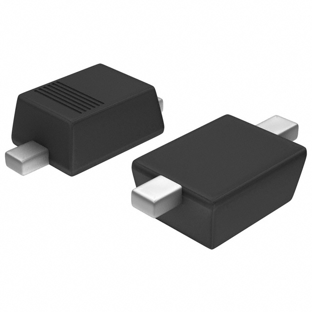
Planar Maximum Efficiency General Application (MEGA) Schottky barrier rectifier with an
integrated guard ring for stress protection, encapsulated in a SOD323F (SC-90) small and
flat lead Surface-Mounted Device (SMD) plastic package.
1.2 Features
n
n
n
n
n
Average forward current: IF(AV) ≤ 0.2 A
Reverse voltage: VR ≤ 40 V
Low forward voltage
AEC-Q101 qualified
Small and flat lead SMD plastic package
1.3 Applications
n
n
n
n
n
n
Low voltage rectification
High efficiency DC-to-DC conversion
Switch Mode Power Supply (SMPS)
Reverse polarity protection
Ultra high-speed switching
Low power consumption applications
1.4 Quick reference data
Table 1.
Quick reference data
Tj = 25 °C unless otherwise specified.
Symbol
Parameter
Conditions
IF(AV)
average forward current
square wave;
δ = 0.5;
f = 20 kHz
Tamb ≤ 130 °C
Tsp ≤ 145 °C
[1]
Min
Typ
Max
Unit
-
-
0.2
A
-
-
0.2
A
VR
reverse voltage
-
-
40
V
VF
forward voltage
IF = 0.2 A
-
520
600
mV
IR
reverse current
VR = 40 V
-
0.7
10
µA
[1]
Device mounted on a ceramic Printed-Circuit Board (PCB), Al2O3, standard footprint.
�PMEG4002EJ
NXP Semiconductors
200 mA low VF MEGA Schottky barrier rectifier
2. Pinning information
Table 2.
Pinning
Pin
Description
1
cathode
2
anode
Simplified outline
Graphic symbol
[1]
1
1
2
2
sym001
[1]
The marking bar indicates the cathode.
3. Ordering information
Table 3.
Ordering information
Type number
PMEG4002EJ
Package
Name
Description
Version
SC-90
plastic surface-mounted package; 2 leads
SOD323F
4. Marking
Table 4.
Marking codes
Type number
Marking code
PMEG4002EJ
1N
5. Limiting values
Table 5.
Limiting values
In accordance with the Absolute Maximum Rating System (IEC 60134).
Symbol
Parameter
Conditions
Min
Max
Unit
VR
reverse voltage
Tj = 25 °C
-
40
V
IF(AV)
average forward current
square wave;
δ = 0.5;
f = 20 kHz
-
0.2
A
Tamb ≤ 130 °C
Tsp ≤ 145 °C
-
0.2
A
IFRM
repetitive peak forward
current
tp ≤ 1 ms;
δ ≤ 0.25
-
2.6
A
IFSM
non-repetitive peak
forward current
square wave;
tp = 8 ms
[2]
-
2.75
A
Ptot
total power dissipation
Tamb ≤ 25 °C
[3][4]
-
385
mW
[3][5]
-
695
mW
[3][1]
-
1045
mW
PMEG4002EJ_1
Product data sheet
[1]
© NXP B.V. 2009. All rights reserved.
Rev. 01 — 15 May 2009
2 of 13
�PMEG4002EJ
NXP Semiconductors
200 mA low VF MEGA Schottky barrier rectifier
Table 5.
Limiting values …continued
In accordance with the Absolute Maximum Rating System (IEC 60134).
Symbol
Parameter
Tj
Conditions
Min
Max
Unit
junction temperature
-
150
°C
Tamb
ambient temperature
−55
+150
°C
Tstg
storage temperature
−65
+150
°C
[1]
Device mounted on a ceramic PCB, Al2O3, standard footprint.
[2]
Tj = 25 °C prior to surge.
[3]
Reflow soldering is the only recommended soldering method.
[4]
Device mounted on an FR4 PCB, single-sided copper, tin-plated and standard footprint.
[5]
Device mounted on an FR4 PCB, single-sided copper, tin-plated, mounting pad for cathode 1 cm2.
6. Thermal characteristics
Table 6.
Thermal characteristics
Symbol
Parameter
Conditions
Rth(j-a)
thermal resistance from
junction to ambient
in free air
Rth(j-sp)
thermal resistance from
junction to solder point
Typ
Max
Unit
[3]
-
-
325
K/W
[4]
-
-
180
K/W
[5]
-
-
120
K/W
[6]
-
-
25
K/W
[1]
For Schottky barrier diodes thermal runaway has to be considered, as in some applications the reverse
power losses PR are a significant part of the total power losses.
[2]
Reflow soldering is the only recommended soldering method.
[3]
Device mounted on an FR4 PCB, single-sided copper, tin-plated and standard footprint.
[4]
Device mounted on an FR4 PCB, single-sided copper, tin-plated, mounting pad for cathode 1 cm2.
[5]
Device mounted on a ceramic PCB, Al2O3, standard footprint.
[6]
Soldering point of cathode tab.
PMEG4002EJ_1
Product data sheet
Min
[1][2]
© NXP B.V. 2009. All rights reserved.
Rev. 01 — 15 May 2009
3 of 13
�PMEG4002EJ
NXP Semiconductors
200 mA low VF MEGA Schottky barrier rectifier
006aab476
103
duty cycle =
Zth(j-a)
(K/W)
1
0.75
0.5
102
0.33
0.25
0.2
0.1
0.05
10
0.02
0.01
0
1
10−5
10−4
10−3
10−2
10−1
1
10
102
103
tp (s)
FR4 PCB, standard footprint
Fig 1.
Transient thermal impedance from junction to ambient as a function of pulse duration; typical values
006aab477
103
Zth(j-a)
(K/W)
duty cycle =
1
0.75
102
0.5
0.33
0.25
0.2
0.1
0.05
10
0.02
0.01
0
1
10−5
10−4
10−3
10−2
10−1
1
10
102
103
tp (s)
FR4 PCB, mounting pad for cathode 1 cm2
Fig 2.
Transient thermal impedance from junction to ambient as a function of pulse duration; typical values
PMEG4002EJ_1
Product data sheet
© NXP B.V. 2009. All rights reserved.
Rev. 01 — 15 May 2009
4 of 13
�PMEG4002EJ
NXP Semiconductors
200 mA low VF MEGA Schottky barrier rectifier
006aab478
103
Zth(j-a)
(K/W)
duty cycle =
1
102
0.75
0.5
0.33
0.25
0.2
0.1
10
0.05
0.02
0.01
0
1
10−5
10−4
10−3
10−2
10−1
1
102
10
103
tp (s)
Ceramic PCB, Al2O3, standard footprint
Fig 3.
Transient thermal impedance from junction to ambient as a function of pulse duration; typical values
7. Characteristics
Table 7.
Characteristics
Tj = 25 °C unless otherwise specified.
Symbol
Parameter
Conditions
Min
Typ
Max
Unit
VF
forward voltage
IF = 0.1 mA
-
190
220
mV
IF = 1 mA
-
250
290
mV
IF = 10 mA
-
320
360
mV
IF = 100 mA
-
440
500
mV
IF = 200 mA
-
520
600
mV
VR = 10 V
-
0.2
0.3
µA
VR = 25 V
-
0.3
0.5
µA
VR = 40 V
-
0.7
10
µA
-
14
-
pF
-
6
-
pF
-
5
-
ns
IR
Cd
reverse current
diode capacitance
f = 1 MHz
VR = 1 V
VR = 10 V
trr
[1]
reverse recovery time
When switched from IF = 10 mA to IR = 10 mA; RL = 100 Ω; measured at IR = 1 mA.
PMEG4002EJ_1
Product data sheet
[1]
© NXP B.V. 2009. All rights reserved.
Rev. 01 — 15 May 2009
5 of 13
�PMEG4002EJ
NXP Semiconductors
200 mA low VF MEGA Schottky barrier rectifier
006aab488
1
IF
(A)
10−1
(1)
006aab489
10−3
IR
(A)
10−4
(1)
10−5
(2)
(2)
10−6
10−2
(3)
(4)
(5)
10−7
(3)
10−8
10−3
10−9
(4)
10−10
10−4
0
0.2
0.4
0.6
0
10
VF (V)
20
30
40
VR (V)
(1) Tj = 150 °C
(1) Tj = 125 °C
(2) Tj = 125 °C
(2) Tj = 85 °C
(3) Tj = 85 °C
(3) Tj = 25 °C
(4) Tj = 25 °C
(4) Tj = −40 °C
(5) Tj = −40 °C
Fig 4.
Forward current as a function of forward
voltage; typical values
Fig 5.
Reverse current as a function of reverse
voltage; typical values
006aab490
30
Cd
(pF)
20
10
0
0
10
20
30
40
VR (V)
f = 1 MHz; Tamb = 25 °C
Fig 6.
Diode capacitance as a function of reverse voltage; typical values
PMEG4002EJ_1
Product data sheet
© NXP B.V. 2009. All rights reserved.
Rev. 01 — 15 May 2009
6 of 13
�PMEG4002EJ
NXP Semiconductors
200 mA low VF MEGA Schottky barrier rectifier
006aab491
0.20
PF(AV)
(W)
PR(AV)
(W)
(4)
0.15
006aab492
0.20
0.15
(3)
(2)
0.10
(1)
0.10
(1)
(2)
(3)
0.05
0.05
0.0
0.0
(4)
0.0
0.1
0.2
0.3
0
10
20
30
IF(AV) (A)
Tj = 150 °C
Tj = 125 °C
(1) δ = 0.1
(1) δ = 1
(2) δ = 0.2
(2) δ = 0.9
(3) δ = 0.5
(3) δ = 0.8
(4) δ = 1
(4) δ = 0.5
Fig 7.
Average forward power dissipation as a
function of average forward current; typical
values
006aab493
0.3
Fig 8.
Average reverse power dissipation as a
function of reverse voltage; typical values
006aab494
0.3
(1)
IF(AV)
(A)
(1)
IF(AV)
(A)
(2)
(2)
0.2
0.2
(3)
(3)
(4)
0.1
(4)
0.1
0.0
0.0
0
25
50
75
100
125
150
175
Tamb (°C)
0
25
50
Tj = 150 °C
100
125
150
175
Tamb (°C)
Tj = 150 °C
(1) δ = 1; DC
(1) δ = 1; DC
(2) δ = 0.5; f = 20 kHz
(2) δ = 0.5; f = 20 kHz
(3) δ = 0.2; f = 20 kHz
(3) δ = 0.2; f = 20 kHz
(4) δ = 0.1; f = 20 kHz
(4) δ = 0.1; f = 20 kHz
Average forward current as a function of
ambient temperature; typical values
Fig 10. Average forward current as a function of
ambient temperature; typical values
PMEG4002EJ_1
Product data sheet
75
FR4 PCB, mounting pad for cathode 1 cm2
FR4 PCB, standard footprint
Fig 9.
40
VR (V)
© NXP B.V. 2009. All rights reserved.
Rev. 01 — 15 May 2009
7 of 13
�PMEG4002EJ
NXP Semiconductors
200 mA low VF MEGA Schottky barrier rectifier
006aab495
0.3
(1)
IF(AV)
(A)
006aab496
0.3
(1)
IF(AV)
(A)
(2)
(2)
0.2
0.2
(3)
(3)
(4)
0.1
(4)
0.1
0.0
0.0
0
25
50
75
100
125
150
175
Tamb (°C)
0
25
50
75
100
125
150
175
Tsp (°C)
Tj = 150 °C
Ceramic PCB, Al2O3, standard footprint
Tj = 150 °C
(1) δ = 1; DC
(1) δ = 1; DC
(2) δ = 0.5; f = 20 kHz
(2) δ = 0.5; f = 20 kHz
(3) δ = 0.2; f = 20 kHz
(3) δ = 0.2; f = 20 kHz
(4) δ = 0.1; f = 20 kHz
(4) δ = 0.1; f = 20 kHz
Fig 11. Average forward current as a function of
ambient temperature; typical values
Fig 12. Average forward current as a function of
solder point temperature; typical values
8. Test information
tr
t
D.U.T.
RS = 50 Ω
tp
10 %
+ IF
IF
V = VR + IF × RS
SAMPLING
OSCILLOSCOPE
trr
t
Ri = 50 Ω
VR
(1)
90 %
mga881
input signal
output signal
(1) IR = 1 mA
Input signal: reverse pulse rise time tr = 0.6 ns; reverse voltage pulse duration tp = 100 ns; duty cycle δ = 0.05
Oscilloscope: rise time tr = 0.35 ns
Fig 13. Reverse recovery time test circuit and waveforms
PMEG4002EJ_1
Product data sheet
© NXP B.V. 2009. All rights reserved.
Rev. 01 — 15 May 2009
8 of 13
�PMEG4002EJ
NXP Semiconductors
200 mA low VF MEGA Schottky barrier rectifier
P
t2
duty cycle δ =
t1
t2
t1
t
006aaa812
Fig 14. Duty cycle definition
The current ratings for the typical waveforms as shown in Figure 9, 10, 11 and 12 are
calculated according to the equations: I F ( AV ) = I M × δ with IM defined as peak current,
I RMS = I F ( AV ) at DC, and I RMS = I M × δ with IRMS defined as RMS current.
8.1 Quality information
This product has been qualified in accordance with the Automotive Electronics Council
(AEC) standard Q101 - Stress test qualification for discrete semiconductors, and is
suitable for use in automotive applications.
9. Package outline
1.35
1.15
0.80
0.65
0.5
0.3
1
2.7
2.3
1.8
1.6
2
0.40
0.25
Dimensions in mm
0.25
0.10
04-09-13
Fig 15. Package outline SOD323F (SC-90)
PMEG4002EJ_1
Product data sheet
© NXP B.V. 2009. All rights reserved.
Rev. 01 — 15 May 2009
9 of 13
�PMEG4002EJ
NXP Semiconductors
200 mA low VF MEGA Schottky barrier rectifier
10. Packing information
Table 8.
Packing methods
The indicated -xxx are the last three digits of the 12NC ordering code.[1]
Type number
Package
Description
PMEG4002EJ SOD323F
[1]
Packing quantity
4 mm pitch, 8 mm tape and reel
3000
10000
-115
-135
For further information and the availability of packing methods, see Section 14.
11. Soldering
3.05
2.2
2.1
solder lands
solder resist
0.5 (2×)
1.65 0.95
0.6 (2×)
solder paste
occupied area
0.5
(2×)
0.6
(2×)
Dimensions in mm
sod323f_fr
Reflow soldering is the only recommended soldering method.
Fig 16. Reflow soldering footprint SOD323F (SC-90)
PMEG4002EJ_1
Product data sheet
© NXP B.V. 2009. All rights reserved.
Rev. 01 — 15 May 2009
10 of 13
�PMEG4002EJ
NXP Semiconductors
200 mA low VF MEGA Schottky barrier rectifier
12. Revision history
Table 9.
Revision history
Document ID
Release date
Data sheet status
Change notice
Supersedes
PMEG4002EJ_1
20090515
Product data sheet
-
-
PMEG4002EJ_1
Product data sheet
© NXP B.V. 2009. All rights reserved.
Rev. 01 — 15 May 2009
11 of 13
�PMEG4002EJ
NXP Semiconductors
200 mA low VF MEGA Schottky barrier rectifier
13. Legal information
13.1 Data sheet status
Document status[1][2]
Product status[3]
Definition
Objective [short] data sheet
Development
This document contains data from the objective specification for product development.
Preliminary [short] data sheet
Qualification
This document contains data from the preliminary specification.
Product [short] data sheet
Production
This document contains the product specification.
[1]
Please consult the most recently issued document before initiating or completing a design.
[2]
The term ‘short data sheet’ is explained in section “Definitions”.
[3]
The product status of device(s) described in this document may have changed since this document was published and may differ in case of multiple devices. The latest product status
information is available on the Internet at URL http://www.nxp.com.
13.2 Definitions
Draft — The document is a draft version only. The content is still under
internal review and subject to formal approval, which may result in
modifications or additions. NXP Semiconductors does not give any
representations or warranties as to the accuracy or completeness of
information included herein and shall have no liability for the consequences of
use of such information.
Short data sheet — A short data sheet is an extract from a full data sheet
with the same product type number(s) and title. A short data sheet is intended
for quick reference only and should not be relied upon to contain detailed and
full information. For detailed and full information see the relevant full data
sheet, which is available on request via the local NXP Semiconductors sales
office. In case of any inconsistency or conflict with the short data sheet, the
full data sheet shall prevail.
13.3 Disclaimers
General — Information in this document is believed to be accurate and
reliable. However, NXP Semiconductors does not give any representations or
warranties, expressed or implied, as to the accuracy or completeness of such
information and shall have no liability for the consequences of use of such
information.
Right to make changes — NXP Semiconductors reserves the right to make
changes to information published in this document, including without
limitation specifications and product descriptions, at any time and without
notice. This document supersedes and replaces all information supplied prior
to the publication hereof.
Suitability for use — NXP Semiconductors products are not designed,
authorized or warranted to be suitable for use in medical, military, aircraft,
space or life support equipment, nor in applications where failure or
malfunction of an NXP Semiconductors product can reasonably be expected
to result in personal injury, death or severe property or environmental
damage. NXP Semiconductors accepts no liability for inclusion and/or use of
NXP Semiconductors products in such equipment or applications and
therefore such inclusion and/or use is at the customer’s own risk.
Applications — Applications that are described herein for any of these
products are for illustrative purposes only. NXP Semiconductors makes no
representation or warranty that such applications will be suitable for the
specified use without further testing or modification.
Limiting values — Stress above one or more limiting values (as defined in
the Absolute Maximum Ratings System of IEC 60134) may cause permanent
damage to the device. Limiting values are stress ratings only and operation of
the device at these or any other conditions above those given in the
Characteristics sections of this document is not implied. Exposure to limiting
values for extended periods may affect device reliability.
Terms and conditions of sale — NXP Semiconductors products are sold
subject to the general terms and conditions of commercial sale, as published
at http://www.nxp.com/profile/terms, including those pertaining to warranty,
intellectual property rights infringement and limitation of liability, unless
explicitly otherwise agreed to in writing by NXP Semiconductors. In case of
any inconsistency or conflict between information in this document and such
terms and conditions, the latter will prevail.
No offer to sell or license — Nothing in this document may be interpreted
or construed as an offer to sell products that is open for acceptance or the
grant, conveyance or implication of any license under any copyrights, patents
or other industrial or intellectual property rights.
Export control — This document as well as the item(s) described herein
may be subject to export control regulations. Export might require a prior
authorization from national authorities.
Quick reference data — The Quick reference data is an extract of the
product data given in the Limiting values and Characteristics sections of this
document, and as such is not complete, exhaustive or legally binding.
13.4 Trademarks
Notice: All referenced brands, product names, service names and trademarks
are the property of their respective owners.
14. Contact information
For more information, please visit: http://www.nxp.com
For sales office addresses, please send an email to: salesaddresses@nxp.com
PMEG4002EJ_1
Product data sheet
© NXP B.V. 2009. All rights reserved.
Rev. 01 — 15 May 2009
12 of 13
�PMEG4002EJ
NXP Semiconductors
200 mA low VF MEGA Schottky barrier rectifier
15. Contents
1
1.1
1.2
1.3
1.4
2
3
4
5
6
7
8
8.1
9
10
11
12
13
13.1
13.2
13.3
13.4
14
15
Product profile . . . . . . . . . . . . . . . . . . . . . . . . . . 1
General description. . . . . . . . . . . . . . . . . . . . . . 1
Features . . . . . . . . . . . . . . . . . . . . . . . . . . . . . . 1
Applications . . . . . . . . . . . . . . . . . . . . . . . . . . . 1
Quick reference data. . . . . . . . . . . . . . . . . . . . . 1
Pinning information . . . . . . . . . . . . . . . . . . . . . . 2
Ordering information . . . . . . . . . . . . . . . . . . . . . 2
Marking . . . . . . . . . . . . . . . . . . . . . . . . . . . . . . . . 2
Limiting values. . . . . . . . . . . . . . . . . . . . . . . . . . 2
Thermal characteristics. . . . . . . . . . . . . . . . . . . 3
Characteristics . . . . . . . . . . . . . . . . . . . . . . . . . . 5
Test information . . . . . . . . . . . . . . . . . . . . . . . . . 8
Quality information . . . . . . . . . . . . . . . . . . . . . . 9
Package outline . . . . . . . . . . . . . . . . . . . . . . . . . 9
Packing information. . . . . . . . . . . . . . . . . . . . . 10
Soldering . . . . . . . . . . . . . . . . . . . . . . . . . . . . . 10
Revision history . . . . . . . . . . . . . . . . . . . . . . . . 11
Legal information. . . . . . . . . . . . . . . . . . . . . . . 12
Data sheet status . . . . . . . . . . . . . . . . . . . . . . 12
Definitions . . . . . . . . . . . . . . . . . . . . . . . . . . . . 12
Disclaimers . . . . . . . . . . . . . . . . . . . . . . . . . . . 12
Trademarks . . . . . . . . . . . . . . . . . . . . . . . . . . . 12
Contact information. . . . . . . . . . . . . . . . . . . . . 12
Contents . . . . . . . . . . . . . . . . . . . . . . . . . . . . . . 13
Please be aware that important notices concerning this document and the product(s)
described herein, have been included in section ‘Legal information’.
© NXP B.V. 2009.
All rights reserved.
For more information, please visit: http://www.nxp.com
For sales office addresses, please send an email to: salesaddresses@nxp.com
Date of release: 15 May 2009
Document identifier: PMEG4002EJ_1
�


 工商网监
湘ICP备2023018690号
工商网监
湘ICP备2023018690号

