JST3401
-30V,-4.2A
P-Channel Mosfet
FEATURES
SOT-23
RDS(ON)≤ 63mΩ @VGS=-10V
RDS(ON)≤ 67mΩ @VGS=-4.5V
RDS(ON)≤ 85mΩ @VGS=-2.5V
APPLICATIONS
Load/Power Switching
Interfacing Switching
P-CHANNEL MOSFET
MARKING
Maximum ratings (Ta=25℃ unless otherwise noted)
Parameter
Symbol
Value
Drain-Source Voltage
VDS
-30
Gate-Source Voltage
VGS
±12
Continuous Drain Current
ID
-4.2
Pulsed Drain Current
IDM
-12
Maximum Power Dissipation
PD
0.4
W
RθJA
313
℃/W
Junction Temperature
TJ
150
Storage Temperature
Tstg
-55 ~+150
Thermal Resistance from Junction to Ambient(t ≤5s)
Unit
V
A
℃
1/4
�JST3401
MOSFET ELECTRICAL CHARACTERISTICS Ta=25 ℃ unless otherwise specified
Parameter
Symbol
Test Condition
Min
Typ
Max
Units
Static
Drain-source breakdown voltage
V(BR)DSS
VGS = 0V, ID =-250µA
-30
-35
Gate-source threshold voltage
VGS(th)
VDS =VGS, ID =-250µA
-0.5
-0.9
-1.5
V
Gate-source leakage
IGSS
VDS =0V, VGS =±12V
±100
nA
Zero gate voltage drain current
IDSS
VDS =-30V, VGS =0V
-1
µA
Drain-source on-state resistance
a
RDS(on)
VGS =-10V, ID =-4.2A
45
63
VGS =-4.5V, ID =-4A
49
67
60
85
-0.7
-1
VGS =-2.5V, ID =-1A
Body diode voltage
IS=-0.7A
VSD
mΩ
V
Dynamic
b
Input capacitance
Ciss
Output capacitance
Coss
Reverse transfer capacitance
Crss
Total gate charge
Qg
Gate-source charge
Qgs
Gate-drain charge
Qgd
Turn-on delay time
td(on)
Rise time
Turn-off delay time
Fall time
1050
VDS =-15V,VGS =0V,f =1MHz
tr
td(off)
pF
127
85
VDS=-15V,VGS=-4.5V
ID=-4A
9.5
nC
2
3
VDS=-15V, RL=3.6Ω,
VGS=-10V,RGEN=6Ω
tf
6.5
3.5
40
nS
13
Notes :
a. Pulse Test : Pulse Width < 300µs, Duty Cycle ≤2%.
b. Guaranteed by design, not subject to production testing.
2/4
�JST3401
P-Channel -30V (D-S) MOSFET Typical Characteristics
3/4
�JST3401
SOT-23 package
SOT-23 Suggested Pad Layout
4/4
�
很抱歉,暂时无法提供与“JST3401”相匹配的价格&库存,您可以联系我们找货
免费人工找货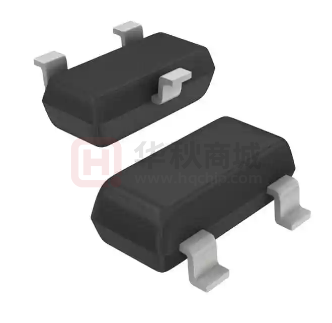


 工商网监
湘ICP备2023018690号
工商网监
湘ICP备2023018690号
