5X7 Dot Character VFD Module
q
q
q
q
q
q
q
q
q
4 X 20 Characters 5mm High
LCD Compatible Design
Operating Temp -40° C to +85° C
Single 5V Supply with Power Save Mode
High Brightness Blue Green Display
Selectable 4/8 bit M68/i80 Interface
ASCII + Extended Character Font
8 User Definable Character RAM
4 Level Brightness Control Function
1
CU20045SCPB-W5J
The module includes the Vacuum Fluorescent Display
glass, driver and micro-controller ICs with refresh RAM,
character generator and interface logic.
The high speed 8 bit parallel interface is 5V CMOS
compatible suitable for connection to a host CPU bus
which can be set to M68 or i80 series interface by a solder
link on the module. Brightness control and power down
functions are provided. A full data sheet is available.
14 x ∅ 1.0
14
20.9 55.0 60.0
19.5
11.1
70.8
93.0
98.0
Dimensions in mm & subject to tolerances. Mounting holes 2.5mm dia.
ELECTRICAL SPECIFICATION
Parameter
Symbol
Value
Condition
Power Supply Voltage
V CC
5.0VDC +/- 5%
GND=0V
Power Supply Current
ICC
275mADC typ.
Vcc=5V
Logic High Input (DB0-DB7)
V IH1
Vss+2.2VDC min. V CC=5V
Logic Low Input (DB0-DB7)
V IL1
Vss+0.6VDC max V CC=5V
Logic High Input (RS,R/W,E) V IH2
0.7 V CC min.
V CC=5V
Logic Low Input (RS,R/W,E)
V IL2
0.3 V CC max.
V CC=5V
Logic High Output
V OH
Vcc-0.6VDC min. IOH = -1.6mA
Logic Low Output
V OL
Vss+0.6VDC max IOL =1.6mA
2.5
3.0
max
1.6
2.5
14.0 max
CHARACTER FONT
The power on rise time should be less than 50ms.The inrush current at power on can be 2 x ICC .
The Icc current is 10mA maximum while in power down mode.
OPTICAL and ENVIRONMENTAL SPECIFICATIONS
Parameter
Value
Character Size/Pitch (XxY mm)
2.4 x 4.7/3.6 x 5.4
Dot Size/Pitch (XxY mm)
0.4 x 0.5/0.5 x 0.7
Luminance
700 cd/m2 (204 fL) Typ.
Colour of Illumination
Blue-Green (Filter for more colours)
Operating Temperature
-40°C to +85°C
Storage Temperature
-50°C to +85°C
Operating Humidity (non condensing) 20 to 80% RH @ 25°C
SOFTWARE COMMANDS
Instruction
R/W
Clear Display
L
Cursor Return Home
L
Entry Mode Set
L
Display ON/OFF
L
Cursor/Display Shift
L
Function Set
L
Brightness Set
L
Set CG RAM Addr.
L
Set DD RAM Addr.
L
Read BUSY/Addr.
H
Write Data to RAM
L
Read Data from RAM H
RS
L
L
L
L
L
L
H
L
L
L
H
H
D0-D7
01H
02H-03H
04H-07H
08H-0FH
10H-1FH
20H-3FH
00H-03H
40H-7FH
80H-E7H
00H-FFH
00H-FFH
00H-FFH
PIN CONNECTIONS
Pin
Sig
Pin
1
GND
2
3
(FNC) 4
5
R/W # 6
7
D0
8
9
D2
10
11
D4
12
13
D6
14
Sig
V CC
RS
E#
D1
D3
D5
D7
TIMING PARAMETERS (min)
(E) nable Cycle Time
666ns
(E) nable Pulse Width 300ns
Hold after (E) nable
10ns
NORITAKE ITRON VFD MODULES
JUMPER LINKS
CONTACT
# Interface M68/i80
When jumper link JP9 is
soldered, these inputs
change to i80 series CPU
control lines.
Pin 5= /WR Pin 6 = /RD
Noritake Sales Office Tel Nos
Nagoya Japan: +81 (0)52-561-9867
Canada: +1-416-291-2946
Chicago USA: +1-847-439-9020
Munchen (D): +49 (0)89-3214-290
Itron UK: +44 (0)1493 601144
Rest Europe: +49 (0)61-0520-9220
Pin 3 (Fnc) Input
www.noritake-itron.com
This is normally open circuit.
Subject to change without notice.
If pads JP2.1 and JP2.2 are
IUK Doc Ref: 03443 Iss:1 11 July 2001
linked. Pin 3 = /Reset.
4x20, 5mm Dot Character
�
很抱歉,暂时无法提供与“CU20045SCPB-W5J”相匹配的价格&库存,您可以联系我们找货
免费人工找货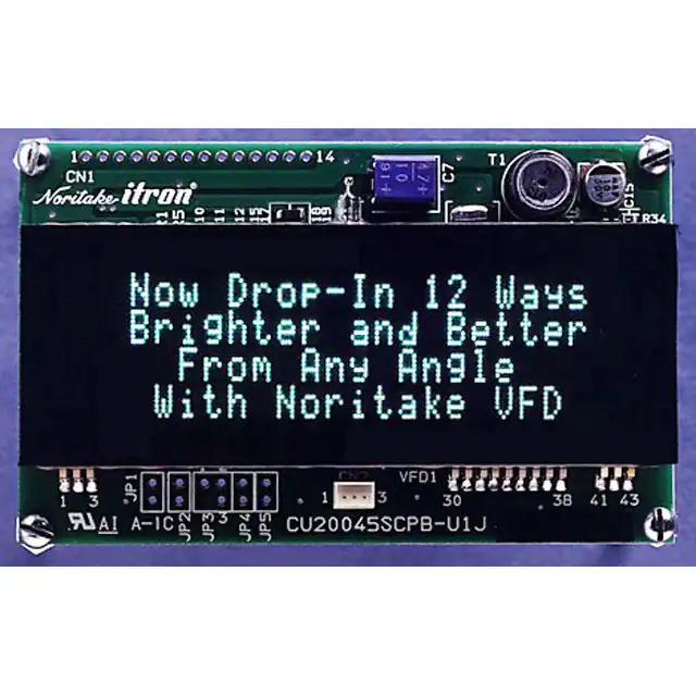


 工商网监
湘ICP备2023018690号
工商网监
湘ICP备2023018690号
