ON TAT INDUSTRIAL COMPANY
SPECIFICATION
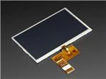
Product Model : YX700WV03 (Rev.A)
Designed by
R&D Checked by
Quality Department
by
Approval by Customer
OK
NG,Problem survey:
Approved By
All Rights Reserved
1/18
Approved by
�ON TAT INDUSTRIAL COMPANY
Revision Record
REV NO.
REV DATE
CONTENTS
A
2014-12-08
NEW ISSUE
All Rights Reserved
2/18
Note
REV A
�ON TAT INDUSTRIAL COMPANY
Table Of Contents
List
Description
Page No.
Cover
1
Revision Record
2
Table Of Contents
3
1
Numbering System
4
2
General Information
4
3
External Dimensions
5
4
Interface Descrirtion
6
5
Absolute Maximum Ratings
6
6
Electrical Characteristics
6
7
Timing Characteristics
7
8
Backlight Charasterics
10
9
Optical Characteristics
11
10
Reliability Test Conditions And Methods
13
11
Inspection Standard
14
12
Handling Precautions
17
13
Precaution For Use
18
14
Packing Method
18
All Rights Reserved
3/18
REV A
�ON TAT INDUSTRIAL COMPANY
1. Numbering System
2. General Iinformation
ITEM
STANDARD VALUES
UNITS
LCD type
7.0’’TFT
--
Dot arrangement
800×3(RGB)×480
dots
Color Pixel Arrangement
RGB vertical stripe
--
Display Mode
TN / Transmissive / Normally white
--
12 o’clock
--
Module size
164.9(W)×100.0(H)×3.4(T)
mm
Active area
154.08(W)×85.92(H)
mm
Dot pitch
0.1926 (W)×0.1790 (H)
mm
Interface
24-bit Parallel RGB Interface
--
Operating temperature
-20 ~ +70
℃
Storage temperature
-30 ~ +80
℃
Weight
TBD
g
Viewing Direction
All Rights Reserved
4/18
REV A
�ON TAT INDUSTRIAL COMPANY
3. External Dimensions
34.08±0.5
(80.96)
164.9±0.3(LCM OUTLINE)
156.7(BEZEL OPEN)
155.08(TP A.A)
154.08(LCD A.A)
TFT NOTE:
1, LCD TYPE :16.7 COLOR ,TFT
2, VIEWING DIRECTION:12 0'CLOCK
3, BACKLIGHT
1)WHITE LED 18 series connection
4, DPERATION TEMP.:-20°~70°
5, STORAGE TEMP.:-30°~80°
(5.49)
(6.4)
(6.9)
导通面
3.4±0.2
补强面
0.3±0.05
(FPC+PI)
A
K
XR
YD
XL
YU
ON TAT INDUSTRIAL COMPANY
REV A
5/18
All Rights Reserved
(3.57)
(4.28)
(4.78)
100±0.3(LCM OUTLINE)
89.1(BEZEL OPEN)
86.92(TP A.A)
85.92(LCD A.A)
(47.74)
65±0.5
�ON TAT INDUSTRIAL COMPANY
4. Interface
Pin
Symbol
Description.
1
LED-K
LED backlight (Cathode).
2
LED-A
LED backlight (Anode).
3
GND
Ground.
4
VDD
Power supply.
5~12
R0~R7
Red Data.
13~20
G0~G7
Green Data.
21~28
B0~B7
Blue Data.
29
GND
Ground.
30
DCLK
Dot clock signal input. Latching input data at its rising edge.
31
DISP
Display on/off.
32
HSYNC
Horizontal sync input. Negative polarity.
33
VSYNC
Vertical sync input. Negative polarity.
34
DEN
35
NC
36
GND
Ground.
37
XR
TP Right.
38
YD
TP Bottom.
39
XL
TP Left.
40
YU
TP Up.
Data enable input. Active high to enable the input data bus.
NC.
5. Absolute Maximum Ratings
Item
Symbol
Min.
Max.
Unit
Analog Supply Voltage
VDD
-0.3
5
V
Input Voltage
Vin
-0.3
VDD+0.3
V
Operating Temperature
TOP
-20
70
°C
Storage Temperature
TST
-30
80
°C
Storage Humidity
HD
20
90
%RH
6. DC Characteristics
Item
Symbol
Min.
Typ.
Max.
Unit
Remark
Analog Supply Voltage
VDD
3.0
3.3
3.6
V
-
Input High Voltage
VIH
0.7VDD
-
VDD
V
Digital input pins
Input Low Voltage
VIL
GND
-
0.3VDD
V
Digital input pins
Output High Voltage
VOH
VDD-0.4
-
VDD
V
Digital output pins
Output Low Voltage
VOL
GND
-
VDD+0.4
V
Digital output pins
I/O Leak Current
ILI
-1
-
1
uA
-
All Rights Reserved
6/18
REV A
�ON TAT INDUSTRIAL COMPANY
7. Timing Characteristics
7.1 Power ON/OFF Sequence
Power on sequence (VDDVEEVGH)
Power off sequence (VGHVEEVDD)
7.2 Timing Diagram of interface Signal
Parallel 24-bit RGB Mode
Input Clock and Data Timing Diagram
All Rights Reserved
7/18
REV A
�ON TAT INDUSTRIAL COMPANY
Source output timing diagram
All Rights Reserved
8/18
REV A
�ON TAT INDUSTRIAL COMPANY
All Rights Reserved
9/18
REV A
�ON TAT INDUSTRIAL COMPANY
8. Backlight Charasterics
A
K
Item
Symbol
MIN
TYP MAX
UNIT
Test Condition
Supply Voltage
Vf
9.3
9.9
10.5
V
If=120mA
Supply Current
Luminous Intensity
for LCM
Life Time
If
-
120
180
mA
-
-
300
400
-
Cd/m2
If=120mA
-
20000
-
-
Hr
If=120mA
Backlight Color
All Rights Reserved
White
10/18
REV A
�ON TAT INDUSTRIAL COMPANY
9. Optical Characteristics
Test Conditions:
1. DVDD=3.3V, IL=180mA (Backlight current), the ambient temperature is 25℃.
2. The test systems refer to Note 2.
Note 1: Definition of viewing angle range
Fig. 1 Definition of viewing angle
All Rights Reserved
11/18
REV A
�ON TAT INDUSTRIAL COMPANY
Note 2: Definition of optical measurement system.
The optical characteristics should be measured in dark room. After 30 minutes
operation, the optical properties are measured at the center point of the LCD screen.
(Response time is measured by Photo detector TOPCON BM-7, other items are
measured by BM-5A/Field of view: 1° /Height: 500mm.)
Fig. 2 Optical measurement system setup
Note 3: Definition of Response time
The response time is defined as the LCD optical switching time interval between
“White” state and “Black” state. Rise time (TON) is the time between photo detector
output intensity changed from 90% to 10%. And fall time (TOFF) is the time between
photo detector output intensity changed from 10% to 90%.
Fig. 3 Definition of response time
Note 4: Definition of contrast ratio
Luminance measured when LCD on the " White " state
Contrast ratio(CR) =
Luminance measured when LCD on the " Black " state
Note 5: Definition of color chromaticity (CIE1931)
Color coordinates measured at center point of LCD.
Note 6: All input terminals LCD panel must be ground while measuring the center area
of the panel. The LED driving condition is IL=180mA .
All Rights Reserved
12/18
REV A
�ON TAT INDUSTRIAL COMPANY
10. Reliability Test Conditions And Methods
NO.
①
②
③
④
TEST ITEMS
High Temperature
Storage
Low Temerature
Storage
High Temperature
Operating
Low Temperature
Operating
⑤
Temperature
Cycle(Storage)
⑥
Damp Proof Test
(Storage)
⑦
Vibration Test
⑧
Drooping Test
⑨
ESD Test
TEST CONDITION
INSPECTION AFTER
TEST
80℃±2℃×200Hours
-30℃±2℃×200Hours
Inspection after
2~4hours storage at
70℃±2℃×120Hours
room temperature,the
samples should be free
-20℃±2℃×120Hours
from defects:
1,Air bublle in the LCD.
-20℃
25℃
70℃
2,Sealleak.
(30min)
(5min)
(30min)
3,Non-display.
1cycle
4,Missing segments.
Total 10cycle
5,Glass crack.
50℃±5℃×90%RH×120Hours
6,Current IDD is twice
higher than initial value.
Frequency:10Hz~55Hz~10Hz
7,The surface shall be
Amplitude:1.5M
free from damage.
X,Y,Z direction for total 3hours
8,The electric
(Packing Condition)
Drop to the ground from 1M height charateristic
requirements shall be
one time
satisfied.
every side of carton.
(Packing Condition)
Voltage:±8KV,R:330Ω,C:150PF,Air
Mode,10times
REMARK:
1,The Test samples should be applied to only one test item.
2,Sample side for each test item is 5~10pcs.
3,For Damp Proof Test,Pure water(Resistance>10MΩ)should be used.
4,In case of malfunction defect caused by ESD damage,if it would be recovered to normal
state after resetting,it would be judge as a good part.
5,EL evaluation should be excepted from reliability test with humidity and
temperature:Some defects such as black spot/blemish can happen by natural chemical
reaction with humidity and Fluorescence EL has.
6,Failure Judgment Criterion:Basic Specification Electrical Characteristic,Mechanical
Characteristic,Optical Characteristic.
All Rights Reserved
13/18
REV A
�ON TAT INDUSTRIAL COMPANY
11. Inspection Standard
This standard apply to C-STN/TFT module
1.
Spot check plan:
According to spot check level Ⅱ,MIL-STD-105D Level Ⅱ,the rank of accept or
reject is below:
3A 级、2A 级:major non-conformance:AQL 0.25 minor non-conformance:AQL
0.4
A 级:major non-conformance: AQL 0.65
2.
minor non-conformance: AQL 1.
Inspection condition:
30 degree
Under daylight lamp 20~40W,product distance inspector’eye 30cm,incline
degree 30°。
3.
LCD area define:
A
B C
Area A:display area
Area B:VA area
Area C:out of VA area,not in sight after assemby
Remark :non-conformance at area C,but is OK that isn’t influence raliability of product
& assembly by customer.
All Rights Reserved
14/18
REV A
�ON TAT INDUSTRIAL COMPANY
4. Inspection standard
4.1 Major non-conformance
NO.
Item
Inspection standard
Rate
Function
4.1.1 non-confor
mance
1) No display,display abnormaly
2) Miss line, short
3) B/L no function or function abnormaly
4) TP no function
4.1.2 miss
No matter miss what component
4.1.3 Out of size
Module dimension out of spec
major
4.2 Appearance non-conformance
NO.
Item
Inspection standard
Rate
dot non-conformance defineΦ
y
Φ= ( x y )
x
2
A grade
Most approve q’ty
area
4.2.1
Black or
white
spot
(power
on)
size(mm)
A
B
Φ≤0.10
ignore
0.10<Φ≤0.15
3
0.15<Φ≤0.20
2
0.20<Φ≤0.25
1
0.25<Φ
0
C
Minor
ignore
Most approve 4 damages, dot to dot ≥10mm
A grade
Size(mm)
4.2.2
Black or
white
line
(power
on)
Most approve q’ty
A
B
L(length)
W(width)
ignore
W≤0.03
ignore
L≤5.0
0.03<
W≤0.05
2
L≤3.0
0.05<
W≤0.07
1
0.07<W
Treat with dot
non-conformance
C
Minor
ignore
Most approve 3 damages, line to line ≥10mm
All Rights Reserved
15/18
REV A
�ON TAT INDUSTRIAL COMPANY
4.2.3
Polarizer 1) polarizer attach meet drawing,disallow out of LCD.
position 2) polarizer must cover display area(special require unless)
Minor
(i) crash at side(remark: S=ITO length)
X
Y
Z
≤3.0
≤S
ignore
Crash disallow extend to ITO or seal.
(ii) commonly surface scathe
4.2.4
LCD
non-conf
ormance
Minor
X
Y
Z
≤2.0


 工商网监
湘ICP备2023018690号
工商网监
湘ICP备2023018690号
