HDG204-WiFi 802.11b+g System in Package
Data Sheet
HDG204
WiFi SIP component
�Data Sheet - Preliminary
HDG204
WiFi SIP component
Revision History
Revision
Revision date
Description
PA1
2009-08-22
First issue
PA2
2011-01-11
Revised pin out
PA3
2011-02-18
Added landpattern
PA4
2011-03-11
Updated reference design
PA5
2011-11-24
Added measurements in landpattern
Disclaimer and copyright notice
Information in this document, including URL references, is subject to change without notice.
THIS DOCUMENT IS PROVIDED "AS IS" WITH NO WARRANTIES WHATSOEVER, INCLUDING ANY WARRANTY
OF MERCHANTABILITY, NONINFRINGEMENT, FITNESS FOR ANY PARTICULAR PURPOSE, OR ANY WARRANTY
OTHERWISE ARISING OUT OF ANY PROPOSAL, SPECIFICATION OR SAMPLE. All liability, including liability for
infringement of any proprietary rights, relating to use of information in this document is disclaimed.
No licenses express or implied, by estoppel or otherwise, to any intellectual property rights are granted
herein.
The Wi-Fi Alliance Member Logo is a trademark of the Wi-Fi Alliance.
All trade names, trademarks and registered trademarks mentioned in this document are property of their
respective owners, and are hereby acknowledged.
Copyright © 2009 H&D Wireless AB. All rights reserved.
Rev. PA5 02/2011
1451 - Data Sheet HDG204
Confidential
page 2 ( 36)
�Data Sheet - Preliminary
HDG204
WiFi SIP component
CONTENTS
1
INTRODUCTION ................................................................................................................... 5
1.1 Overview ................................................................................................................................................................... 5
1.2 Key Features ............................................................................................................................................................. 5
2
HARDWARE ARCHITECTURE................................................................................................. 6
2.1 Block Diagram.......................................................................................................................................................... 6
2.2 Order information ................................................................................................................................................... 6
3
ELECTRICAL DATA ................................................................................................................ 7
3.1 Absolute maximum ratings ..................................................................................................................................... 7
3.2 Electro Static Discharge .......................................................................................................................................... 7
3.3 Recommended operating conditions ...................................................................................................................... 7
3.4 Power Consumption ................................................................................................................................................. 8
3.5 RF Performance ....................................................................................................................................................... 9
3.6 Digital pin characteristics ........................................................................................................................................ 9
4
PIN CONFIGURATIONS ....................................................................................................... 14
4.1 Pin Configuration................................................................................................................................................... 14
4.2 Pin assignments ...................................................................................................................................................... 14
5
APPLICATION INFORMATION ............................................................................................. 17
5.1 Power Supply .......................................................................................................................................................... 17
5.2 Clocks ...................................................................................................................................................................... 17
5.3 Reset Pin ................................................................................................................................................................. 18
5.4 Shutdown ................................................................................................................................................................ 18
5.5 Power save .............................................................................................................................................................. 19
5.6 Power On sequence ................................................................................................................................................ 19
5.7 Shut Down sequence .............................................................................................................................................. 21
5.8 Power OFF Sequence ............................................................................................................................................. 22
5.9 Interfaces ................................................................................................................................................................ 22
5.10 RF interface ............................................................................................................................................................ 23
5.11 General application information .......................................................................................................................... 23
5.12 Reference design schematic HDG204 ................................................................................................................... 26
Rev. PA5 02/2011
1451 - Data Sheet HDG204
Confidential
page 3 ( 36)
�Data Sheet - Preliminary
6
HDG204
WiFi SIP component
PACKAGE SPECIFICATIONS ................................................................................................. 28
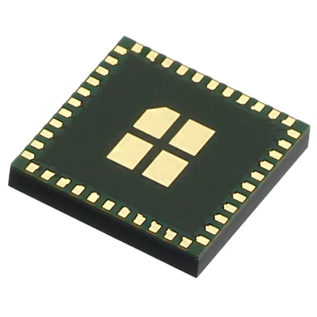
6.1 Mechanical outline QFN 44pin ............................................................................................................................. 28
6.2 Marking HDG204 QFN ......................................................................................................................................... 28
6.3 Package pad dimension ......................................................................................................................................... 29
6.4 Mounting information ........................................................................................................................................... 30
7
TAPE AND REEL INFORMATION .......................................................................................... 31
8
STANDARDS COMPLIANCE ................................................................................................. 32
8.1 IEEE/IETF ............................................................................................................................................................. 32
8.2 WiFi standards ....................................................................................................................................................... 32
8.3 Regulatory .............................................................................................................................................................. 32
9
SALES OFFICES ................................................................................................................... 35
10 REFERENCE DESIGNS ......................................................................................................... 36
10.1 Reference design using HDG204........................................................................................................................... 36
Rev. PA5 02/2011
1451 - Data Sheet HDG204
Confidential
page 4 ( 36)
�Data Sheet - Preliminary
HDG204
WiFi SIP component
1 INTRODUCTION
1.1 Overview
HDG204 is a complete WLAN System In Package, SIP, solution specifically designed to address the
proliferation of Wi-Fi technology into embedded devices. HDG204 enables a cost efficient ultra low power,
high performance and feature rich client solution. It provides up to 54 Mbit/s data rate when operating in
the OFDM mode and up to 11 Mbit/s data rate when operating in the DSSS/CCK mode.
HDG204 integrates RF IC, baseband/MAC IC, EEPROM and RF filters into a highly integrated and optimized
SIP (System In Package) solution with high quality and reliability. This minimizes the need of external
components, simplifying assembly and test.
The integrated circuits are implemented in state of the art processes like SiGe in 0.35um for the radio and
0.13um 1.2V CMOS for the baseband/MAC. This highly integrated solution is optimized for customer
applications running on a host CPU.
The host interface supports SDIO/SPI and UART. Internal RAM comprises both code and data memory
eliminating the need for external RAM, Flash or ROM memory interfaces. Baseband firmware, FW, is stored
on the host and downloaded at start up. MAC address, trimming values etc are stored in the on board
EEPROM.
1.2 Key Features
Data Rates: 1, 2, 5.5, 6, 9, 11, 12, 18, 24, 36, 48, and 54Mbps
Modulation: QPSK, 16QAM, 64QAM DBPSK, DQPSK, CCK, OFDM with BPSK
WEP and AES hardware encryption accelerator up to 128 bits
Adjustable output power. Max +18dBm (CCK).
Advanced on-chip RF filter
Selection (DFS) for spectrum management and Transmit Power Control (TPC).
Low power consumption due to efficient class AB PA design
LDO:s for RF-VCO and crystal oscillator for lower pushing
Support for an external 32kHz real time clock
Extensive DMA hardware support for data flow to reduce CPU load.
External clock 40MHz supported, internal trimming capacitors allows the use of low cost
crystal
Internal Boot-ROM. This allows firmware to be downloaded into SRAM from the host
Advanced power management for optimum power consumption at varying load.
External interfaces SDIO/SPI
Power Supplies 3.3 V and 1.2 V
Small footprint 8 x 8 mm (64 mm2), height 1.4 mm max
RoHS Compliant
Rev. PA5 02/2011
1451 - Data Sheet HDG204
Confidential
page 5 ( 36)
�Data Sheet - Preliminary
HDG204
WiFi SIP component
2 HARDWARE ARCHITECTURE
2.1 Block Diagram
Figure 2.1: Block diagram.
2.2 Order information
.
Part No.
Clock option
Package
Shipment package
HDG204-DN-2
External clock support
QFN 44+4 pins, 8.0 x 8.0 mm
Tape & Reel
HDG204-DN-3
External clock support
QFN 44+4 pins, 8.0 x 8.0mm
Tray
Table 2-1: Order information.
Rev. PA5 02/2011
1451 - Data Sheet HDG204
Confidential
page 6 ( 36)
�Data Sheet - Preliminary
HDG204
WiFi SIP component
3 ELECTRICAL DATA
3.1 Absolute maximum ratings
Rating
Min
Max
Unit
Supply voltage
0
4
V
Supply voltage I/O
0
4
V
10
dBm
+125
o
C
260
o
C
Input RF level
Storage temperature
-50
Lead temperature (No Pb), solder 40sek*)
Table 3-1:Absolute maximum ratings. Exceeding any of the maximum ratings, even briefly lead to deterioration in
performance or even destruction. Values indicates condition applied one at the time.
*Ref. IPC/JEDEC J-STD-020C, July 2004
3.2 Electro Static Discharge
HDG204 withstands ESD voltages up to 2000 V tested with HBM (Human Body Model)
according to JESD22-A114 and up to 300 V tested with MM (Machine Model) according to
JESD22-A115.
3.3 Recommended operating conditions
Rating
Min
Typ.
Max
Unit
Supply Voltage VCC
2.75
3.3
3.6
V
Supply Voltage VBAT_P
2.7
VBAT_P0.6
3.3
3.6
V
3.3
3.6
V
Supply Voltage VBAT_32K
Supply Voltage VPA
2.7
3.3
3.6
V
Supply Voltage, DVDD
1.15
1.20
1.25
V
Supply Voltage VDD_IO, VDD_SDIO
1.7
3.3
3.6
V
Operating temperature
-40
+25
+85
o
C
Table 3-2: Recommended operating conditions
Rev. PA5 02/2011
1451 - Data Sheet HDG204
Confidential
page 7 ( 36)
�Data Sheet - Preliminary
HDG204
WiFi SIP component
3.4 Power Consumption
3.4.1 Current Consumption
Mode
Conditions
Supply Pin
Voltage
All modes
VBAT_P+VCC+
VPA+VBAT_32K
All modes
Min
Typ.
Max
Unit
3.6 V
250
mA
VPA
3.6 V
150
mA
All modes
VBAT_P+VCC
3.6 V
150
mA
All modes
DVDD
1.2 V
100
mA
All modes
25ºC
VBAT_32K
3.3 V
10
μA
Tx
25ºC
DVDD
1.2 V
15
mA
Rx
25ºC
1.2 V
60
mA
Sleep
25ºC
DVDD
VBAT_P+VCC+
VPA+VBAT_32K
3.3 V
30
μA
Sleep
25ºC
25ºC DVDD
OFF
DVDD
VBAT_P+VCC+
VPA+VBAT_32K
1.2 V
110
μA
3.3 V
15
μA
Shutdown
Table 3-3: Current consumption in different modes
3.4.2 Power Consumption
Tamb=25°C, VCC=VBAT_P=VBAT_32K=VPA=3.3 V, DVDD =1.2 V
Mode
Output Power
Power Consumption
Comments
TX 802.11b
+17 dBm
725 mW
1, 2, 5.5, 11 Mbit/s
TX 802.11g
+14 dBm
590 mW
6, 9, 12, 18, 24, 36, 48, 54 Mbit/s
RX 802.11b
N/A
220 mW
RX 802.11g
N/A
230 mW
Power Save
N/A
0,4 mW
Sleep
N/A
0,2 mW
Receive only, 2s RX beacons
No receive, FW loaded, only LFC
running
Shutdown
N/A
0,05 mW
No FW loaded, DVDD OFF
Table 3-4: Power consumption in different modes.
Rev. PA5 02/2011
1451 - Data Sheet HDG204
Confidential
page 8 ( 36)
�Data Sheet - Preliminary
HDG204
WiFi SIP component
3.5 RF Performance
VCC=VPA= 2.75 – 3.6V, DVDD=1.15 - 1.25V External supply, Tamb= -40 – +85°C
Parameter
Conditions
Min
Frequency range
Typical
2400
RF impedance
Max
Units
2500
MHz
50
ohm
TRANSMITTER PERFORMANCE
Output power
QPSK
+16,5
+17
+17,5
dBm
Output power
OFDM 54Mbit/s
+13,5
+14
+14,5
dBm
EVM at +15dBm
QPSK
30
35
%
EVM at +11dBm
OFDM 54MBit/s
3.5
5
%
Receiver sensitivity
DPSK 1Mbit/s
-96
dBm
Receiver sensitivity
QDPSK 2Mbit/s
-92
dBm
Receiver sensitivity
CCK/DPSK 5.5Mbit/s
-91
dBm
Receiver sensitivity
CCK/BPSKK 11Mbit/s
-88
dBm
Receiver sensitivity
OFDM 6Mbit/s
-91
dBm
Receiver sensitivity
OFDM 9Mbit/s
-90
dBm
Receiver sensitivity
OFDM 12Mbit/s
-88
dBm
Receiver sensitivity
OFDM 18Mbit/s
-86
dBm
Receiver sensitivity
OFDM 24Mbit/s
-83
dBm
Receiver sensitivity
OFDM 36Mbit/s
-80
dBm
Receiver sensitivity
OFDM 48Mbit/s
-76
dBm
Receiver sensitivity
OFDM 54Mbit/s
-74
dBm
RECEIVER PERFORMANCE
Table 3-5: RF performance
3.6 Digital pin characteristics
3.6.1 SDIO timing characteristics
The SDIO/SPI-interface can run in two different modes, Default mode and High speed mode.
SDIO 1-bit default mode is selected at Power On Reset. The default mode is showed in
Fig. 3.6.1 and table: 3.6. For the high speed mode see Fig. 3.2 and table: 3.7. Condition:
VDDIO= 1.7 – 3.6 V, TA= -40 – +85°C
Rev. PA5 02/2011
1451 - Data Sheet HDG204
Confidential
page 9 ( 36)
�Data Sheet - Preliminary
HDG204
WiFi SIP component
Figure 3-1: SDIO/SPI timing diagram (default mode)
Parameter
Symbol
Min
Input set-up time
tISU
5
ns
Input hold time
tIH
5
ns
Clock fall time
tTHL
10
ns
Clock rise time
tTLH
10
ns
Output delay time
tODLY
14
ns
0
Max
Unit
Comments
Table 3-6: SDIO timing parameter values (default mode)
Figure 3-2: SDIO timing diagram (high speed mode)
Rev. PA5 02/2011
1451 - Data Sheet HDG204
Confidential
page 10 ( 36)
�Data Sheet - Preliminary
HDG204
Parameter
Symbol
Clock fall time
WiFi SIP component
Min
Max
Unit
tTHL
3
ns
Clock rise time
tTLH
3
ns
Output delay time
tODLY
2,5
14
ns
Output hold time
tOH
2.5
Comments
ns
Table 3-7: SDIO timing parameter values (high speed mode)
3.6.2 Digital input IPU and IPD
IPU (Input pin with pull-up) Input with internal pull-up includes a high impedance input buffer. The input
has pull-up that ensures that the pad is detected as high if it is left open.
IPD (Input pin with pull-down) Input with an internal pull-down includes a high impedance input buffer. The
input has a pull-down that ensures that the pad is detected as high if it is left open.
Both configurations are also protected against over-voltages and ESD with a protection circuitry, see Figure
3-3. The pins configured according to this are stated IPU and IPD under Type in Table 4-1.
Figure 3-3: Function schematics of the IPU and IPD input pad configurations.
Parameter
Symbol
Min
Typ.
Input low voltage
VIL
-0.3
0.25*VIO V
Input high voltage
Input leakage
current
Input pin
capacitance
VIH
0.625*VIO
VIO+0.3
V
IIL
-1
1
μA
VDDIO, VDD_SDIO
VIO
CIP
Max
2,5
1.7
Units
Comments
pF
3,6
V
Table 3-8: IPU and IPD pin DC characteristics.
Rev. PA5 02/2011
1451 - Data Sheet HDG204
Confidential
page 11 ( 36)
�Data Sheet - Preliminary
HDG204
WiFi SIP component
3.6.3 Digital input/output pad (I/O)
The I/O pin functional schematic is stated in Fig. 3.4. It includes an input buffer and an output buffer with
an enable/disable bit. No pull-up or pull-down is available on this type of pad.
Figure 3-4: Function schematics of the I/O input pad configuration.
Parameter
Symbol
Min
Input low voltage
VIL
Input high voltage
Input leakage
current
Output low voltage
VOL
Output high voltage
Input pin
capacitance
VOH
VDDIO, VDD_SDIO
VIO
Typ.
Max
Units
-0.3
0.25*VIO
V
VIH
0.625*VIO
VIO+0.3
V
IIL
-1
1
μA
0.125*VIO V
0.75*VIO
CIP
V
2.5
1.7
Comments
Iout-1mA
pF
3.6
V
Table 3-9: I/O pin DC characteristics
3.6.4 Protection digital pins
All digital pins are protected against over-voltage with a “snap-back” circuit connected between the pad
and GND. The “snap-back” voltage is 6.2 V and the holding voltage is 6 V. This provides a satisfying
protection against over voltages and ESD. Also there is a diode included to protect against reversed
voltages.
Rev. PA5 02/2011
1451 - Data Sheet HDG204
Confidential
page 12 ( 36)
�Data Sheet - Preliminary
HDG204
WiFi SIP component
3.6.5 Analogue input A1 and A2
There are two different analogue input pad types. One (A1) for I/O using higher voltages than 1.8 V and
another (A2) for I/O using voltages below 1.8 V (i.e. supplied from the 1.2 V supply), see schematic in Figure
3-5. The A1 is protected with a diode to the supply voltage.
The A2 is protected from voltages above 3 x Vdiode (about 2 V at Ta=25°C)
Figure 3-5: Schematics of analogue inputs A1 and A2
.
One digital input, SHUTDOWN uses the analog pad A1.
SHUTDOWN is a dedicated pin used for controlling the shutdown function.
For pin data see Table 4-1
Parameter
Symbol
Min
Input low voltage
VIL
Input high voltage
Input leakage current
Input current
Typ.
Max
Units
-0.3
0.2
V
VIH
1.5
VBAT_32K+0.3 V
IIL
-1
+1
IIN
2
Comments
μA
mA
During low
to
high
transition
Table 3-10: SHUTDOWN pin DC characteristics.
Rev. PA5 02/2011
1451 - Data Sheet HDG204
Confidential
page 13 ( 36)
�Data Sheet - Preliminary
HDG204
WiFi SIP component
4 PIN CONFIGURATIONS
23
24
25
26
27
28
29
30
31
32
33
4.1 Pin Configuration
39
17
40
16
41
15
42
14
43
13
44
12
6
11
18
10
38
9
19
8
37
7
20
5
36
4
21
3
35
2
22
1
34
Figure 4-1: Package pin out. Top view
4.2 Pin assignments
Pin
Function
Type
Description
1
SDIO CLK
IPU
SDIO Clock, SDIO/SPI CLK
2
SDIO DAT0
I/O
SDIO Data 0, SDIO/SPI MISO
3
SDIO DAT1
I/O
SDIO Data 1, SDIO/SPI IRQ
4
GND
S
Ground
5
ANT_WLAN
RF
Antenna Port (50 Ohm) for WLAN
Rev. PA5 02/2011
1451 - Data Sheet HDG204
Confidential
page 14 ( 36)
�Data Sheet - Preliminary
HDG204
WiFi SIP component
6
GND
S
Ground
7
ICE_TDI
IPU
ICE Test Data Input, do not connect
8
ICE_TRST
IPU
ICE Test Reset, do not connect
9
ICE_TCK
IPU
ICE Test Clock, do not connect
10
NO CONNECTION
-
Do not connect
11
ICE_TMS
IPU
ICE Test Mode Select, do not connect
12
VPA
S
Power supply for RF Power Amplifier
13
ICE_TDO
I/O
ICE Test Data output, do not connect
14
NO CONNECTION
-
Do not connect
15
NO CONNECTION
-
Do not connect
16
NO CONNECTION
-
Do not connect
17
NO CONNECTION
-
18
DVDD
S
Do not connect
DIGITAL VDD 1.2V, de-couple with a 1uF
capacitor to GND
19
NO CONNECTION
-
20
VCC_REG_VCO
S
21
VCC
S
22
NO CONNECTION
-
23
VCC_REG_PLL
S
Do not connect
LDO Decoupling. Connect a 27pF capacitor to
GND
24
SHUTDOWN
A1
Shutdown pin. Active Low
25
I
HFC Oscillator IN
26
40MHz IN/EXT_REF_IN
40MHz OUT/
EXT_REF_OP
O
27
DCDC_ENABLE
A1
28
VDD_CKL_12
S
29
VDD_CKL_26
S
30
VBAT_32K
S
31
TEST_EN
IPD
HFC Oscillator OUT
Connect to GND.
Internal DC/DC not used
HFC X-tal driver decoupling. Connect a 100nF
capacitor to GND
HFC PLL decoupling. Connect a 1uF capacitor to
GND
32 kHz clock supply. Connect a 100nF capacitor
to GND
Test Enable with internal pull down, connect to
GND
32
DCO
S
DC/DC Converter out. Leave open
33
NO CONNECTION
-
34
VBAT_P
S
Do not connect
Main supply 3.3V. De-couple with a 1uF
capacitor to GND
35
RESET_N
IPU
Digital Reset with internal pull up. Active Low
Rev. PA5 02/2011
Do not connect
LDO Decoupling. Connect a 27pF capacitor to
GND
Radio supply 3.3V, de-couple with a 1uF
capacitor to GND
1451 - Data Sheet HDG204
Confidential
page 15 ( 36)
�Data Sheet - Preliminary
HDG204
WiFi SIP component
External Power Control. Connect 100k resistor
to GND
36
EXT_PWR_EN
I/O
37
LFC
I/O
38
VDD_IO
S
32KHz external clock
VDD_IO Supply for digital I/Os except SDIO
domain
39
NO CONNECTION
-
Do not connect
40
SDIO DAT3
I/O
SDIO Data 3, SDIO/SPI CARD_SELECT active low
41
SDIO CMD
I/O
42
VDD_MAC_BB
S
SDIO Command, SDIO/SPI MOSI
Internal 1.2V Decoupling, connect a 330nF
capacitor to GND
43
VDD_SDIO
S
SDIO domain I/O Supply 3.3V
44
SDIO DAT2
I/O
SDIO Data 2
45
GND
S
Ground
45
GND
S
Ground
45
GND
S
Ground
45
GND
S
Ground
Table 4-1: Pin Description for the package.
Rev. PA5 02/2011
1451 - Data Sheet HDG204
Confidential
page 16 ( 36)
�Data Sheet - Preliminary
HDG204
WiFi SIP component
5 APPLICATION INFORMATION
5.1 Power Supply
HDG204 should be powered by dual supplies 3.3V and 1.2V (typical).
5.1.1 Main supply
The main power is connected to the VCC, VBAT_P, VPA and VBAT_32K pins. The ripple on VCC should be
less than 10mV p-p. External decoupling capacitors should be connected, min 1uF on VCC, VBAT_P and
DVDD, min 100nF on VBAT_32K.
The 1.2V supply should be fed externally. Leave the DCO pin open.
5.1.2 Interface Supply
HDG204 has two IO-Supply voltage pins. VDD_SDIO is for the SDIO-bus.
All other I/O-pins are supplied by VDD_IO.
All IO-Supply voltage pins shall be connected to a supply voltage even if some interfaces are not used
5.1.3 Ground pins
The HDG204 is an RF device and requires as such a good RF grounding. Connect pin 3 and the four pads in
the bottom center, pins 45-48, to GND.
5.2 Clocks
5.2.1 High Frequency Clock, HFC
The circuit has an internal oscillator driver that only needs a 40 MHz external crystal and one capacitor to
generate the clock signal. The crystal is connected between the pins 40MHz_IN and 40MHz_OUT. A 0.5 pF
capacitor should be connected between the 40MHz_IN and 40MHz_OUT pins. The crystal should be placed
as close as possible to the circuit pins. Stray capacitances to GND for crystal interconnect traces should be
as small as possible. See Figure 5-1
Parameter
Condition
Min
Typ.
Max
Unit
Frequency
40
MHz
CL
8
pF
Cm
3.5
6.0
fF
C0 (shunt cap)
0.5
2.0
pF
Equiv Rs
0
60
ohm
Frequency tolerance
Ta=25 °C
-15
15
ppm
Freq vs temp
Ta= -40 – +85 °C
-15
15
ppm
Table 5-1: Recommended crystal parameters
Rev. PA5 02/2011
1451 - Data Sheet HDG204
Confidential
page 17 ( 36)
�Data Sheet - Preliminary
HDG204
WiFi SIP component
Condition Min Max Unit
Figure 5-1: Reference clock setup
5.2.2 Low frequency clock, LFC
HDG204 utilize an external 32 kHz clock for keeping Real Time. It is connected to the
LFC_IN pin. Internal Real Time is kept by FW, calibrating the LFC against the more accurate HFC in runtime.
Thus a fairly wide LFC frequency range can be used.
Parameter
Min
Typ.
Max
Unit
LFC frequency
30
32
34
kHz
Clock accuracy
-2000
2000
ppm
Duty cycle
30
70
%
50
Note
Table 5-2: External LFC requirements
5.3 Reset Pin
The RESET_N pin is active low. It has an internal pull-up, can be left unconnected. Pulling the
RESET_N pin low resets all digital logic.
Note: An internal RESET is generated at Power On with the same function as pulling the RESET_N pin low.
All VBAT power supply pins must be discharged close to GND, typically below 0.2 Volt, for this Power On
Reset to be generated at a following Power On.
5.4 Shutdown
The SHUTDOWN pin shall be set high during normal operation. Pulling the SHUTDOWN pin low, sets
HDG204 in Shutdown mode. This turns OFF most parts of the circuit and minimizes the current
consumption. All I/O interface pins are set to predefined states (high, low or high-z) when in Shutdown
mode. For minimum power consumption keep VBAT_P and VCC ON but turn DVDD, external 1.2 V, OFF
while the SHUTDOWN pin is low.
To end Shutdown mode set SHUTDOWN pin high and reload FW.
Rev. PA5 02/2011
1451 - Data Sheet HDG204
Confidential
page 18 ( 36)
�Data Sheet - Preliminary
HDG204
WiFi SIP component
For more information regarding the use of SHUTDOWN refer to Power On sequence and Shutdown
sequence.
Note: During Power ON, with SHUTDOWN low, before loading of FW, pin EXT_PWR_EN is high and all other
I/O-pins are high-z. With SDHUTDOWN high, load FW and let it start, then when SHUTDOWN is set low all
I/O-pins will be set according to their FW defaults.
Application Information
5.5 Power save
Power save is an energy saving mode where HDG204 is only listening at regular intervals for the beacons
transmitted from an access point and is set in sleep mode in between. During this sleep mode, FW is kept in
RAM but all not needed functions are turned off. Since the receive time is very short compared to the
listening interval the average current consumption is reduced significantly.
The timing of the listening interval is based on the LFC (32 kHz) clock. See Low frequency clock, LFC.
Pin EXT_PWR_EN is set high at initial Power ON, independent of pins RESET and SHUTDOWN, before FW is
loaded. FW then sets it low. This pin is not further used in the present FW. During HW Shutdown this pin is
in-determent, set to output low or to high z. Thus if HW Shutdown is used, connected it to a 100K pull
down resistor.
5.6 Power On sequence
The HDG204 Power On sequence is described in timing diagram Figure 5-2 and Table 5-3 berlow.
Figure 5-2: Start up sequence with 40 MHz crystal and FW loaded from host via SDIO.
Rev. PA5 02/2011
1451 - Data Sheet HDG204
Confidential
page 19 ( 36)
�Data Sheet - Preliminary
HDG204
Parameter
Symbol
Min
VDDIO turn on time
tVDDIO
0
ms
Shut down disable time
tSHUTDOWN
0
ms
VBAT set up time
tVBAT_SU
-0.2 *
tSHUTDOWN
DVDD set up time
tVDD_P_SU
-0.2 *
tSHUTDOWN
Reset time
tRESET
2
ms
SPI_EN0 turn low time
40 MHz OSC start up
time
tSPIEN_L
0.02
ms
tXTAL_ST
2.5
BB1 HW start up time 1
tBB1
3
ms
At 32.768 kHz
BB2 HW start up time 2
Firmware loading Delay
time
tBB2
7
ms
At HFC 40 MHz
Firmware loading time
tFW_LOAD
tFW_LOAD_D
Typ.
WiFi SIP component
Max
Unit
ms
ms
100
External 1.2 V
supply
ms
ms
20
Comment
ms
At HFC 40 MHz
SDIO clock and host
SW dependent
Table 5-3: Start up timing using 40 MHz crystal and FW load from host
*. SHUTDOWN-pin can be set high slightly before VBAT_P, VCC or DVDD, this makes it possible to use the SHUTDOWN signal as
enable for external LDO:s for these supplies
Rev. PA5 02/2011
1451 - Data Sheet HDG204
Confidential
page 20 ( 36)
�Data Sheet - Preliminary
HDG204
WiFi SIP component
5.7 Shut Down sequence
The following shutdown procedure shall be used for a shutdown and start up sequence of the HDG204,
when a 40MHz crystal is used. FW are reloaded from the host when restarting from SHUTDOWN. Note that
all supply voltages are ON during shutdown except DVDD which must be tuned OFF. VPA can optionally be
turned OFF. See timing diagram Fig. 5.4 and Table 5.6
Figure 5-3: Shut down and start up sequence with 40 MHz crystal osc. and FW loaded from host.
Parameter
Symbol
Min
FW loading delay time
tFW_LOAD_D
20
FW loading time
tFW_LOAD
Typ.
Max
Unit
Comment
ms
100
ms
SDIO clock and host
SW dependent.
Table 5-4: Shutdown timing with external 1.2 V supply, crystal and FW load from host.
Rev. PA5 02/2011
1451 - Data Sheet HDG204
Confidential
page 21 ( 36)
�Data Sheet - Preliminary
HDG204
WiFi SIP component
5.8 Power OFF Sequence
All power supplies can be turned OFF at the same time.
If not turned OFF simultaneously the sequence in Figure 5.5 below should be followed.
Figure 5-4: Power OFF Sequence
Parameter
Symbol
Min
Typ.
VDDIO turn off time
VBAT_P , VCC, VPA
turn off times
tVDDIO_OFF
0
tVBAT_OFF
tVDDIO_OFF
DVDD turn OFF time
SHUTDOWN,
DCDC_ENABLE turn
OFF time
tDVDD_OFF
tVBAT_OFF
tINPUTS_OFF
0
IO-pins to High-Z time
tIO_Z
0
Max
Unit
Comment
μs
μs
μs
ms
Table 5-5: Power OFF timing
5.9 Interfaces
The HDG204 is equipped with a number of interfaces that can be set up in various ways.
5.9.1 Host Interface SDIO/SPI
The SDIO-bus pins can be used as SDIO or SPI
Default at Power On Reset is SDIO 1-bit mode. Host Software must send the appropriate command in SDIO
1-bit mode to change to SDIO 4-bit mode or to SDIO SPI-mode.
All unused interface pins shall be left open. For timing characteristics and trigger level see
Figure 3-1: SDIO/SPI timing diagram (default mode)Figure 3-1and Table 3-6 or Figure 3-2 and Table 3-7
Rev. PA5 02/2011
1451 - Data Sheet HDG204
Confidential
page 22 ( 36)
�Data Sheet - Preliminary
HDG204
WiFi SIP component
5.9.2 Host Wake Up
To wake up the host if the HDG204 detects an event it can wake up the host via SDIO DAT1 (pin2) of the
SDIO interface. This is the normal wake up and is implemented in the FW.
5.10 RF interface
The RF output pin impedance is 50 ohm and shall be connected to an antenna with VSWR much better than
2:1.
5.11 General application information
5.11.1
Design directions
The design using the HDG204 must be performed according to good RF design considerations. All the leads
shall be as short as possible between the circuit pins and the external components. Highest priority has the
RF-port to antenna strip line, the 40MHz x-tal connections and the VBAT_P decoupling capacitor.
5.11.2
Soldering
The HDG204 uses a QFN package. The recommended solder profile is pictured in Figure 5.6.
To lower the moister content bake the packages for 192 hours at 40–45°C and 220ºC
30-60 s
240255ºC
>220ºC
30-60 s
240255ºC
>217ºC
60-90 s
240255ºC
Cool
Down
Zone
Peak125ºC
No
Peak125ºC
< 1ºC/s
Comment
O2< 500ppm
Peak125ºC
< 1ºC/s
Table 5-6: Reflow Zones
5.11.3
Environmental statement
The HDG204 is designed and manufactured to comply with the RoHS and Green directives.
Rev. PA5 02/2011
1451 - Data Sheet HDG204
Confidential
page 25 ( 36)
�Data Sheet - Preliminary
HDG204
WiFi SIP component
5.12 Reference design schematic HDG204
Figure 5-6: Reference design schematic.
Rev. PA5 02/2011
1451 - Data Sheet HDG204
Confidential
page 26 ( 36)
�Data Sheet - Preliminary
5.12.1
HDG204
WiFi SIP component
Reference Design power supplies
Requirements with SHUTDOWN pin Low
HDG204 pin
State
VPA
ON or OFF
VCC, VBAT_P
ON
VBAT_32K
ON
DVDD
OFF
VDDIO
ON
SDIO DAT0, SDIO DAT1,
SDIO DAT2, SDIO DAT3
Output High
Figure 5-7: Reference Design power supplies
Rev. PA5 02/2011
1451 - Data Sheet HDG204
Confidential
page 27 ( 36)
�Data Sheet - Preliminary
HDG204
WiFi SIP component
6 Package Specifications
6.1 Mechanical outline QFN 44pin
8.0 mm
8.0 mm


 工商网监
湘ICP备2023018690号
工商网监
湘ICP备2023018690号
