Additional Resources:
Product Page
|
3D Model
date
08/30/2021
page
1 of 7
SERIES: PYB30-U │ DESCRIPTION: DC-DC CONVERTER
FEATURES
•
•
•
•
•
•
•
•
•
•
up to 30 W isolated output
industry standard pinout
4:1 input range (9~36 Vdc, 18~75 Vdc)
smaller package
single/dual/triple regulated outputs
1,500 Vdc isolation
continuous short circuit, over current protection, over voltage protection
temperature range (-40~85°C)
six-sided metal shielding
efficiency up to 90%
MODEL
input
voltage
output
voltage
output
current
output
power
ripple
and noise1
efficiency
typ
(Vdc)
range
(Vdc)
(Vdc)
min
(mA)
max
(mA)
max
(W)
max
(mVp-p)
typ
(%)
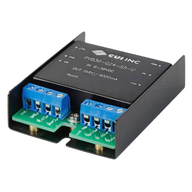
PYB30-Q24-S5-U
24
9~36
5
300
6000
30
100
88
PYB30-Q24-S12-U
24
9~36
12
125
2500
30
100
88
PYB30-Q24-S15-U
24
9~36
15
100
2000
30
100
90
PYB30-Q24-D5-U
24
9~36
±5
±150
±3000
30
100
86
PYB30-Q24-D12-U
24
9~36
±12
±63
±1250
30
100
89
PYB30-Q24-D15-U
24
9~36
±15
±50
±1000
30
100
90
175
±31
3500
±625
26.5
100
85
PYB30-Q24-T312-U
24
9~36
3.3
±12
PYB30-Q24-T315-U
24
9~36
3.3
±15
175
±25
3500
±500
26.5
100
86
PYB30-Q24-T512-U
24
9~36
5
±12
150
±31
3000
±625
30
100
88
PYB30-Q24-T515-U
24
9~36
5
±15
150
±25
3000
±500
30
100
88
PYB30-Q48-S5-U
48
18~75
5
300
6000
30
100
88
PYB30-Q48-S12-U
48
18~75
12
125
2500
30
100
88
PYB30-Q48-S15-U
48
18~75
15
100
2000
30
100
89
PYB30-Q48-D5-U
48
18~75
±5
±150
±3000
30
100
86
PYB30-Q48-D12-U
48
18~75
±12
±63
±1250
30
100
87
PYB30-Q48-D15-U
48
18~75
±15
±50
±1000
30
100
87
175
±31
3500
±625
26.5
100
85
PYB30-Q48-T312-U
48
18~75
3.3
±12
PYB30-Q48-T315-U
48
18~75
3.3
±15
175
±25
3500
±500
26.5
100
85
PYB30-Q48-T512-U
48
18~75
5
±12
150
±31
3000
±625
30
100
88
PYB30-Q48-T515-U
48
18~75
5
±15
150
±25
3000
±500
30
100
87
Notes:
1. Ripple and noise are measured at 20 MHz BW by “parallel cable” method with 1 µF ceramic and 10 µF electrolytic capacitors on the output.
cui.com
�Additional Resources:
Product Page
|
3D Model
CUI Inc │ SERIES: PYB30-U │ DESCRIPTION: DC-DC CONVERTER
date 08/30/2021 │ page 2 of 7
PART NUMBER KEY
PYB30 - QXX - XXX - U
Base Number
Input Voltage
Output
S = single
D = dual
T = triple
Mounting Type
U = U-Frame
Output Voltage
INPUT
parameter
conditions/description
operating input voltage
24 Vdc input models
48 V input models
min
typ
max
units
9
18
24
48
36
75
Vdc
Vdc
start-up voltage
24 Vdc input models
48 Vdc input models (single/dual output models)
48 Vdc input models (triple output models)
9
18
17.8
Vdc
Vdc
Vdc
under voltage shutdown1
24 Vdc input models
48 Vdc input models
7.8
16
surge voltage
for maximum of 1 second
24 Vdc input models
48 Vdc input models
-0.7
-0.7
start-up time
filter
Vdc
Vdc
50
100
Vdc
Vdc
10
ms
1
mA
pi filter
models ON (CTRL open or connect high level, 2.5~12 Vdc)
CTRL2
models OFF (CTRL connect GND or low level, 0~1.2 Vdc)
input current (models OFF)
Notes:
1. Contact CUI if you are planning to use this feature in your application.
2. CTRL pin voltage is referenced to GND.
OUTPUT
parameter
conditions/description
min
line regulation
full load, input voltage from low to high
single and dual output models
triple output models (main output)
triple output models (auxiliary outputs)
load regulation
5% to 100% load, nominal input
single and dual output models
triple output models (main output)
triple output models (auxiliary outputs)
cross regulation
dual output models:
main output 50% load, secondary output from
10% to 100% load
voltage accuracy
single and dual output models
triple output models (main output)
triple output models (auxiliary outputs)
3
adjustability4
typ
max
units
±0.2
±0.5
±1
±5
%
%
%
±0.5
±1
±2
±5
%
%
%
±5
%
±3
±3
±5
%
%
%
±1
±1
±3
±10
%
switching frequency
PWM mode
400
kHz
transient recovery time
25% load step change
300
500
μs
transient response deviation
25% load step change
±3
±5
%
temperature coefficient
100% load, single and dual output models
100% load, triple output models
±0.02
±0.03
%/°C
%/°C
Notes:
3. For dual output models, unbalanced load can not exceed ±5%. If ±5% is exceeded, it may not meet all specifications.
4. Output trimming available on single and dual output models only.
cui.com
�Additional Resources:
Product Page
|
3D Model
CUI Inc │ SERIES: PYB30-U │ DESCRIPTION: DC-DC CONVERTER
date 08/30/2021 │ page 3 of 7
PROTECTIONS
parameter
conditions/description
short circuit protection
hiccup, continuous, automatic recovery
min
over current protection
over voltage protection
3.3 Vdc output models
5 Vdc output models
12 Vdc output models
15 Vdc output models
typ
max
units
150
%
3.9
6.2
15
18
Vdc
Vdc
Vdc
Vdc
SAFETY AND COMPLIANCE
parameter
conditions/description
min
typ
max
isolation voltage
for 1 minute at 1 mA max.
1,500
Vdc
isolation resistance
at 500 Vdc
1,000
MΩ
conducted emissions
CISPR22/EN55022, class A, class B (external circuit required, see Figure 1-b)
radiated emissions
CISPR22/EN55022, class A, class B (external circuit required, see Figure 1-b)
ESD
IEC/EN61000-4-2, class B, contact ± 4kV
radiated immunity
IEC/EN61000-4-3, class A, 10V/m
EFT/burst
IEC/EN61000-4-4, class B, ± 2kV (external circuit required, see Figure 1-a)
surge
IEC/EN61000-4-5, class B, ± 2kV (external circuit required, see Figure 1-a)
conducted immunity
IEC/EN61000-4-6, class A, 3 Vr.m.s
voltage dips & interruptions
IEC/EN61000-4-29, class B, 0%-70%
MTBF
as per MIL-HDBK-217F @ 25°C
RoHS
2011/65/EU
1,000,000
units
hours
ENVIRONMENTAL
parameter
conditions/description
min
max
units
operating temperature
see derating curve
-40
85
°C
-55
125
°C
storage temperature
storage humidity
non-condensing
case temperature
at full load, Ta=71°C
typ
5
95
%
105
°C
max
units
MECHANICAL
parameter
conditions/description
dimensions
67.5 x 54.99 x 19.05
case material
aluminum alloy
min
typ
mm
weight
58
cui.com
g
�Additional Resources:
Product Page
CUI Inc │ SERIES: PYB30-U │ DESCRIPTION: DC-DC CONVERTER
U-FRAME
units: mm[inch]
tolerance: ±0.5[±0.020]
Wire range: 22~14 AWG
DIN rail mounting kit available
(part# STK-DIN)
PIN CONNECTIONS
Single
Output
Dual
Output
Triple
Output
1
Vin
Vin
Vin
2
GND
GND
GND
3
CTRL
CTRL
CTRL
4
Case
Case
Case
5
NC
Trim
-Vo2
6
Trim
-Vo
0V
7
0V
0V
+Vo1
8
+Vo
+Vo
+Vo2
3D Model
date 08/30/2021 │ page 4 of 7
MECHANICAL DRAWING
PIN
|
cui.com
�Additional Resources:
Product Page
|
3D Model
CUI Inc │ SERIES: PYB30-U │ DESCRIPTION: DC-DC CONVERTER
date 08/30/2021 │ page 5 of 7
DERATING CURVES
EMC RECOMMENDED CIRCUIT
single output
Figure 1
Table 1
Recommended external circuit components
Vin (Vdc)
FUSE
24
Choose according to input current
MOV
10D560K
10D101K
LDM
56μH
56μH
TVS
SMCJ48A
SMCJ90A
C0
120μF/50V
120μF/100V
dual output
C1
4.7μF/50V
2.2μF/100V
LCM
2.2mH
2.2mH
C2
4.7μF/50V
2.2μF/100V
C3*
1nF/2kV
1nF/2kV
C4
1nF/2kV
1nF/2kV
*
Note:
triple output
48
*2nF/2kV capacitors for triple output, 48 Vdc input
models.
TEST CONFIGURATION
Table 2
External components
Figure 2
Note:
Input reflected-ripple current is measured with an inductor Lin and Capacitor Cin to simulate source impedance.
cui.com
Lin
4.7μH
Cin
220μF, ESR < 1.0Ω
at 100 kHz
�Additional Resources:
Product Page
|
3D Model
CUI Inc │ SERIES: PYB30-U │ DESCRIPTION: DC-DC CONVERTER
date 08/30/2021 │ page 6 of 7
APPLICATION NOTES
1. Recommended circuit
This series has been tested according to the following recommended testing circuit before leaving the factory. This series should be
tested under load (see Figure 3). If you want to further decrease the input/output ripple, you can increase the capacitance accordingly or choose capacitors with low ESR (see Table 3). However, the capacitance of the output filter capacitor must be appropriate. If
the capacitance is too high, a startup problem might arise. For every channel of the output, to ensure safe and reliable operation, the
maximum capacitance must be less than the maximum capacitive load (see Table 4).
Figure 3
single output
dual output
triple output
Table 3
Single
Vout
(Vdc)
Cin
(µF)
Cout
(µF)
Dual
Vout
(Vdc)
Cin
(µF)
Table 4
Cout1
(µF)
Triple
Vout
(Vdc)
Cin
(µF)
Cout1
(µF)
--
--
--
--
--
--
3.3
10
10
5
10
10
±5
10
10
5
10
10
12
10
4.7
±12
10
4.7
±12
10
4.7
15
10
4.7
±15
10
4.7
±15
10
4.7
Note:
Single
Vout
(Vdc)
Max.
Capacitive
Load
(μF)
Dual
Vout
(Vdc)
Max.
Capacitive
Load1
(μF)
Triple
Vout
(Vdc)
Max.
Capacitive
Load1
(μF)
--
--
--
--
3.3/±12
4700/300
5
6000
5
2000
3.3/±15
4700/220
12
2500
12
1250
5/±12
4700/300
1100
15
680
5/±15
4700/220
15
1. For each output.
Note:
2.
1. For each output.
Output voltage trimming
Leave open if not used.
Figure 4
Application Circuit for Trim pin
(part in broken line is the interior of models)
Formula for Trim Resistor
up : R T=
aR 2
R2-a
-R3
a=
Vref
R1
Vo’ - Vref
down : R T=
aR 1
R1-a
-R3
a=
Vo’ - Vref
R2
Vref
+ Vo
+Vo
R1
V re f
R2
RT
R1
R3
Trim
V re f
RT
R3
R2
0V
0V
Tr im up
Tr im down
Trim
Note: Value for R1, R2, R3, and Vref refer to Table 5
RT: Trim Resistor
a: User-defined parameter, no actual meanings
Vo': The trim up/down voltage
Vout
(Vdc)
Table 5
Note:
R1
(kΩ)
R2
(kΩ)
R3
(kΩ)
Vref
(V)
5
2.883
2.864
10
2.5
12
10.971
2.864
17.8
2.5
15
14.497
2.864
17.8
2.5
1. Minimum load shouldn't be less than 5%, otherwise ripple may increase dramatically. Operation under minimum load will not damage the converter, however, they may
not meet all specifications listed.
2. Maximum capacitive load is tested at input voltage range and full load.
3. All specifications are measured at Ta=25°C, humidity


 工商网监
湘ICP备2023018690号
工商网监
湘ICP备2023018690号
