Additional Resources:
Product Page
|
3D Model
|
PCB Footprint
date
09/22/2021
page
1 of 7
SERIES: V78-1000 │ DESCRIPTION: NON-ISOLATED SWITCHING REGULATOR
FEATURES
•
•
•
•
•
•
•
•
1 A current output
extremely high efficiency up to 97%
no heat sink required
pin compatible to LM78XX linear regulators
available in straight and right angle SIP packages
low ripple and noise
short circuit protection, thermal shutdown
wide temperature (-40~85°C)
RoHS
MODEL
input
voltage
output
voltage1
output
current
ripple
and noise2
efficiency
typ
(Vdc)
range
(Vdc)
(Vdc)
max
(mA)
max
(mVp-p)
Vin min
(%)
Vin max
(%)
V7803-1000
24
4.75~28
3.3
1,000
35
90
83
V7805-1000
24
6.5~32
5
1,000
35
93
88
V7806-1000
24
9~32
6.5
1,000
35
94
90
V7809-1000
24
12~32
9
1,000
35
95
92
V7812-1000
24
16~32
12
1,000
35
96
94
V7815-1000
24
20~32
15
1,000
35
97
94
Notes:
1. Not recommended for use in a negative output mode.
2. Ripple and noise are measured at 20 MHz BW, see Test Configuration section.
PART NUMBER KEY
V78 XX - 1000 X
Base Number
Output Voltage
Output Current
cui.com
"blank" = straight pins
R = 90° pins
�Additional Resources:
Product Page
|
3D Model
|
PCB Footprint
CUI Inc │ SERIES: V78-1000 │ DESCRIPTION: NON-ISOLATED SWITCHING REGULATOR
date 09/22/2021 │ page 2 of 7
INPUT
parameter
conditions/description
min
typ
max
units
operating input voltage
3.3 Vdc model
5 Vdc model
6.5 Vdc model
9 Vdc model
12 Vdc model
15 Vdc model
4.75
6.5
9.0
12
16
20
24
24
24
24
24
24
28
32
32
32
32
32
Vdc
Vdc
Vdc
Vdc
Vdc
Vdc
parameter
conditions/description
min
typ
max
units
line regulation
Vin = min ~ max, at full load
±0.2
±0.4
%
load regulation
measured from 10% load to full load
±0.4
±0.6
%
voltage accuracy
100% load
±2
±3
%
switching frequency
100% load, input voltage range
330
450
OUTPUT
280
temperature coefficient
±0.02
load capacitance
kHz
%/°C
1,000
μF
max
units
PROTECTIONS
parameter
conditions/description
min
short circuit protection
continuous, automatic recovery
thermal shutdown
typ
150
°C
SAFETY AND COMPLIANCE
parameter
conditions/description
MTBF
as per MIL-HDBK-217F, 25°C
RoHS compliant
2011/65/EU
min
typ
max
2,000,000
units
hours
ENVIRONMENTAL
parameter
conditions/description
min
operating temperature
see derating curve
storage temperature
case temperature
storage humidity
non-condensing
lead temperature
1.5 mm from case for 10 seconds
cui.com
typ
max
units
-40
85
°C
-55
125
°C
100
°C
95
%
300
°C
�Additional Resources:
Product Page
|
3D Model
|
PCB Footprint
CUI Inc │ SERIES: V78-1000 │ DESCRIPTION: NON-ISOLATED SWITCHING REGULATOR
date 09/22/2021 │ page 3 of 7
DERATING CURVES
MECHANICAL
parameter
conditions/description
dimensions
11.50 x 9.00 x 17.50 (0.689 x 0.354 x 0.453 inch)
min
case material
plastic (UL94-V0)
typ
max
units
mm
weight
3.7
g
MECHANICAL DRAWING
units: mm [inches]
tolerance: ±0.25 [0.010]
pin section tolerance: ±0.10 [0.004]
V78XX-1000
V78XX-1000R
11.50[0.453]
17.50 [0.689]
0.50 [0.020]
17.50 [0.689]
1.50
[0.059]
4.10 [0.161]
(Bottom View)
1.00 [0.039]
2
3
0.30
[0.012]
0.50 [0.020]
1 2
3
1
2.54 [0.100]
1
2.15 [0.085]
(Bottom View)
2.15
[0.085]
4.10[0.161]
2.15
[0.085]
5.08 [0.200]
5.08 [0.200]
5.08 [0.200]
9.00 [0.354]
2
5.08 [0.200]
9.00 [0.354]
0.50 [0.020]
11.50[0.453]
3
2.54 [0.100]
1.00 [0.039]
PIN CONNECTIONS
PIN
FUNCTION
1
+Vin
2
GND
3
+Vo
cui.com
1.35 [0.053]
�Additional Resources:
Product Page
|
3D Model
|
PCB Footprint
CUI Inc │ SERIES: V78-1000 │ DESCRIPTION: NON-ISOLATED SWITCHING REGULATOR
date 09/22/2021 │ page 4 of 7
EXTERNAL CAPACITOR TABLE
Part Number
C12 (Ceramic capacitor)
C2 (Ceramic capacitor)
V7803-1000(R)
10μF/50V
22μF/6.3V
V7805-1000(R)
10μF/50V
22μF/16V
V7806-1000(R)
10μF/50V
10μF/16V
V7809-1000(R)
10μF/50V
10μF/16V
V7812-1000(R)
10μF/50V
10μF/25V
V7815-1000(R)
10μF/50V
10μF/25V
TYPICAL APPLICATION CIRCUIT
Notes:
1. C1 and C2 are required and should be fitted close to the converter pins.
2. If the input voltage is greater than 26 Vdc (3.3 Vdc output model) or greater than 28 Vdc (all other models), it is required to have C1 be ≥ 22 µF electrolytic capacitor to
protect the part from voltage spikes.
OUTPUT RIPPLE REDUCTION
1
C1
DC/DC
3
Converter
2
L
+Vout
C2
22 F
GND
To reduce output ripple, it is recommended to add a LC filter in output port.
L: Recommended parameter 10 H ~ 47 H.
cui.com
Load
Vin
�Additional Resources:
Product Page
|
3D Model
CUI Inc │ SERIES: V78-1000 │ DESCRIPTION: NON-ISOLATED SWITCHING REGULATOR
EFFICIENCY AND RIPPLE CURVES
cui.com
|
PCB Footprint
date 09/22/2021 │ page 5 of 7
�Additional Resources:
Product Page
|
3D Model
|
PCB Footprint
CUI Inc │ SERIES: V78-1000 │ DESCRIPTION: NON-ISOLATED SWITCHING REGULATOR
TEST CONFIGURATION
Efficiency and Output Voltage Ripple Test
Start-up and Load Transient Response Test
Note:
All specifications measured at 25°C, humidity
很抱歉,暂时无法提供与“V7815-1000”相匹配的价格&库存,您可以联系我们找货
免费人工找货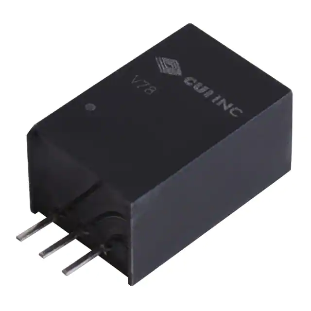


 工商网监
湘ICP备2023018690号
工商网监
湘ICP备2023018690号

