IQ Switch®
ProxSense® Series
ProxSense® IQS333 Datasheet
9 Channel Projected / 7 Channel Self- Capacitive Touch and Proximity
Controller with 2 x 11-bit slider/scroll wheels
The IQS333 ProxSense® IC is a 9-channel projected (or 7-channel self) capacitive proximity
and touch controller with best in class sensitivity, signal to noise ratio and power consumption.
Other features include automatic tuning of sense electrodes, internal reference capacitor and
internal regulator to reduce total system cost.
Main Features
7 Self or 9 Mutual Channel Capacitive Controller
2 Configurable 11-bit sliders/scroll wheels
Advanced on-chip digital signal processing
Automatic adjustment for optimal performance (ATI)
RoHS2
Compliant
User selectable Proximity and Touch thresholds
Long proximity range
Automatic drift compensation
Fast I2C Interface
Event mode or Streaming modes
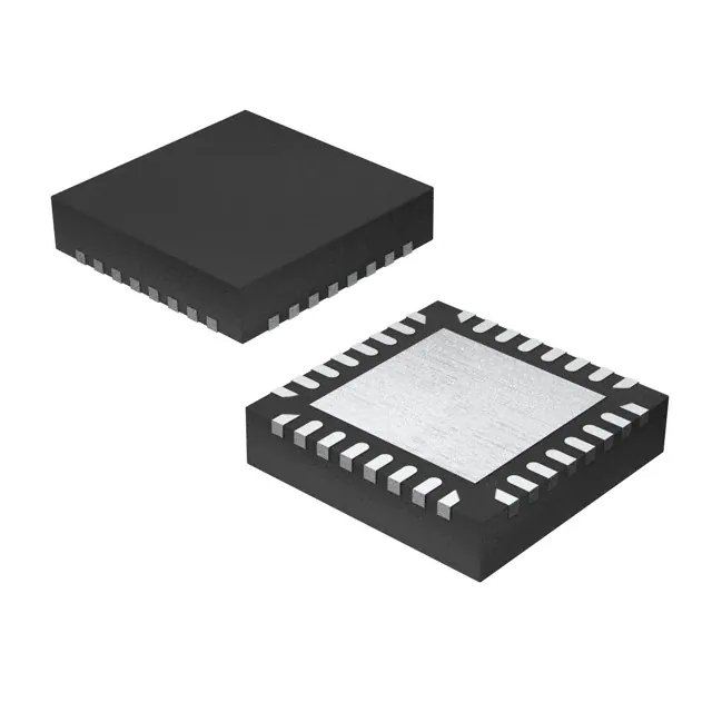
IQS333 QFR32
Representations only, not
actual markings
8 PWM LED/Output drivers (5mA source/10mA sink)
o Hardware PWM set through I2C memory map – no overhead from host
o Dimming modes available, up and down
o Minimum, maximum & adjustable limit levels for dimming modes
Low Power, suitable for battery applications
Supply voltage: 1.8V to 3.6V
LTA + Threshold
Turbo Mode: See Section 5.10.2
Target Values: Lower target values
requires shorter charge transfer
times (tSENSE), thus reducing the
SCAN PERIOD and increasing the
touch report rate.
Threshold can be either a Proximity or
Touch threshold, depending on the current
channel being processed.
Copyright © Azoteq (Pty) Ltd 2019.
All rights reserved.
IQS333 Datasheet
Revision 1.14
Page 20 of 56
February 2020
�IQ Switch®
ProxSense® Series
Note that a proximity condition will be
forced enabled if there is a touch condition
on any channel.
Please refer to Section 1.1 and 5.4 for
proximity and touch threshold selections.
6.6 ATI
The Automatic Tuning Implementation
(ATI) is a sophisticated technology
implemented on the new ProxSense®
series devices. It allows for optimal
performance of the devices for a wide
range of sense electrode capacitances,
without modification or addition of external
components.
The ATI allows the tuning of two
parameters, an ATI Multiplier and an ATI
Compensation, to adjust the Count values
for an attached sense electrode.
ATI allows the designer to optimize a
specific design by adjusting the sensitivity
and stability of each channel through the
adjustment of the ATI parameters.
The IQS333 has a full ATI function. The
full-ATI function is default enabled, but can
be disabled by setting the ATI_OFF bit, or
changed to partial or alternative ATI by
setting the ATI_Partial and ATI_ALT bits in
Register 0x08, byte 0.
The ATI_Busy bit in Register 0x01, byte 0
(Sysflags0) will be set while an ATI event is
busy.
For more information regarding the ATI
algorithm, please contact Azoteq at:
ProxSenseSupport@azoteq.com
𝑆𝑒𝑛𝑠𝑖𝑡𝑖𝑣𝑖𝑡𝑦 ∝
As can be seen from this equation, the
sensitivity can be increased by either
increasing the Target value or decreasing
the Base value. It should, however, be
noted that a higher sensitivity will yield a
higher noise susceptibility.
6.6.2 ATI Target
The target value is reached by adjusting
the COMPENSATION bits for each channel
(ATI target limited to 4096 counts).
The target value is written into the
respective channel’s TARGET registers.
The value written into these registers
multiplied by 8 will yield the new target
value. (Please refer to Section 5.13)
6.6.3 ATI Base (Multiplier)
The base value is calculated with the
compensation set to zero. The following
parameters will influence the base value:
Cs_SIZE1: Size of sampling capacitor.
PROJ_BIAS bits: Adjusts the biasing of
some analogue parameters in the
mutual capacitive operated IC. (Only
applicable in mutual capacitance
mode.)
Charge Transfer Frequency
MULTIPLIER bits.
The base value used for the ATI function
can be implemented in 2 ways:
1. ATI_PARTIAL = 0. ATI automatically
adjusts MULTIPLIER bits to reach a
selected base value2. Please refer
to Section 5.12 for available base
values.
6.6.1 ATI Sensitivity
On the IQS333 device, the user can specify
the BASE value (Section 5.12) for each
channel individually and the TARGET
values (Section 5.13) for the proximity
(CH0) and touch (CH1-CH9) channels.
Sensitivity is a function of base and target
values as follows:
Copyright © Azoteq (Pty) Ltd 2019.
All rights reserved.
𝑇𝐴𝑅𝐺𝐸𝑇
𝐵𝐴𝑆𝐸
1
Changing CS_SIZE if ATI_OFF = 0 will change CS
2
ATI function will use user selected CS_SIZE and
PROJ_BIAS (if applicable) and will only adjust the
MULTIPLIER bits to reach the base values.
IQS333 Datasheet
Revision 1.14
Page 21 of 56
February 2020
�IQ Switch®
ProxSense® Series
2. ATI_PARTIAL = 1. The designer can
specify the multiplier settings. These
settings will give a custom base
value from where the compensation
bits
will
be
automatically
implemented to reach the required
target value. The base value is
determined by two sets of multiplier
bits. Sensitivity Multipliers which will
also scale the compensation to
normalise
the
sensitivity
and
Compensation Multipliers to adjust
the gain.
6.6.4 Re-ATI
An automatic re-ATI event will occur if the
counts are outside its re-ATI limits. The reATI limit or ATI boundary is calculated as
the target value divided by 8. For example:
-
Target = 512, Re-ATI will occur if CS is
outside 512±64.
A re-ATI event can also be issued by the
host MCU by setting the REDO_ATI bit in
Register 0x08, byte0 (ProxSettings0). The
REDO_ATI bit will clear automatically after
the ATI event was started.
Note: Re-ATI will automatically clear all
proximity, touch and halt status bits.
LTAnew = CS + 8 (CS – 8 for Self). The LTA
will then track the CS value until they are
even.
Performing a reseed action on the LTA
filters, will effectively clear any proximity
and/or touch conditions that may have
been established prior to the reseed call.
6.6.6 Alternative ATI
The
Alternative
ATI
implementation
ensures that all the multiplier values are
identical for all the channels and adjusts
only the compensation in order to achieve
the desired count value. The multipliers are
selected from the channel with the smallest
multipliers according to the full ATI
algorithm. Alternative ATI can be enabled
in Register 0x08, byte 0.
6.6.7 ATI ERROR
The ATI error bit (read only) in Register
0x08, byte 1 (Prox_Settings1) indicates to
the user that the ATI targets where not
reached. Adjustments of the base values or
ATI BANDs are required.
6.6.8 ATI Band
The user has the option to select the re-ATI
band as 1/8 of the ATI target (default) or ¼
of the ATI target counts by setting the ATI
BAND bit in Register 0x08, byte 1
(Prox_Settings1).
6.6.5 Reseed
Setting the Reseed bit in Register 0x08,
byte 0), will shift all LTA filters to a value of
7 Communication
The IQS333 device interfaces to a master controller via a 3-wire (SDA, SCL and RDY) serial
interface bus that is I2CTM compatible, with a maximum communication speed of 400kbit/s.
7.1 Control Byte
The Control byte indicates the 7-bit device address (64H default) and the Read/Write indicator
bit. The structure of the control byte is shown in Figure 7.1.
Copyright © Azoteq (Pty) Ltd 2019.
All rights reserved.
IQS333 Datasheet
Revision 1.14
Page 22 of 56
February 2020
�IQ Switch®
ProxSense® Series
7 bit address
MSB
1
1
0
0
1
I2C Group
Figure 7.1
0
0
R/W LSB
Sub- addresses
IQS333 Control Byte.
The I2C device has a 7 bit Slave Address (default 0x64H) in the control byte as shown in
Figure 7.1. To confirm the address, the software compares the received address with the
device address. Sub-address values can be set by OTP programming options.
7.2 I2C Read
To read from the device a current address read can be performed. This assumes that the
address-command is already setup as desired.
Current Address Read
Start
Control Byte
S
Data n
Data n+1
ACK
NACK
ACK
Figure 7.2
Stop
S
Current Address Read.
If the address-command must first be specified, then a random read must be performed. In
this case a WRITE is initially performed to setup the address-command, and then a repeated
start is used to initiate the READ section.
Start
Control Byte
S
Adr + WRITE
Random Read
Addresscommand
ACK
ACK
Figure 7.3
Start
Control Byte
S
Adr + READ
Data n
Stop
NACK
ACK
S
Random Read.
7.3 I2C Write
To write settings to the device a Data Write is performed. Here the Address-Command is
always required, followed by the relevant data bytes to write to the device.
DATA WRITE
Start
Control Byte
S
Adr + WRITE
AddressCommand
ACK
Figure 7.4
Data n
ACK
Data n+1
ACK
Stop
ACK
S
I2C Write.
7.4 End of Communication Session / Window
Similar to other Azoteq I2C devices, to end the I2C communication session, a STOP command
is given. When sending numerous read and write commands in one communication cycle, a
repeated start command must be used to stack them together (since a STOP will jump out of
the communication window, which is not desired).
The STOP will then end the communication, and the IQS333 will return to process a new set of
data. Once this is obtained, the communication window will again become available (RDY set
LOW).
Copyright © Azoteq (Pty) Ltd 2019.
All rights reserved.
IQS333 Datasheet
Revision 1.14
Page 23 of 56
February 2020
�IQ Switch®
ProxSense® Series
7.5 I2C Sub-address
7.7 RDY Hand-Shake Routine
The IQS333 has four available sub
addresses, 64H (default) to 67H, which
allows up to four devices on a single I2C
bus.
The master or host MCU has the capability
to force a communication window at any
time, by pulling the RDY line low. The
communication window will open directly
following the current conversion cycle.
7.5.1 Internal sub-address selection
Selecting the sub-address via OTP bits
allows the user 4 different options:
Table 7.1
I2C sub-address selection
FG25 FG26 Device Address
0
0
1
1
0
1
0
1
0x64
0x65
0x66
0x67
7.6 Event Mode
7.8 I2C Specific Commands
7.8.1 Show Reset
The SHOW_RESET bit can be read in
Register 0x01, byte 1 (Sysflags0), to
determine whether a reset has occurred on
the device. This bit will be set ’1’ after a
reset. A reset can be forced by writing the
Soft_Reset bit in Register 0x08, byte 2
(ProxSettings2).
By default the device operates in full
streaming mode. There is an option for an
event-driven I2C communication mode (also
called “Event Mode”), with the RDY pin
ONLY indicating a communication window
after a prescribed event has occurred.
The SHOW_RESET bit will be cleared (set
to ’0’) by writing a ’1’ into the ACK_RESET
bit
in
Register
0x08,
byte
3
(ProxSettings3). A reset will typically take
place if a timeout during communication
occurs.
These events include:
7.8.2 WDT disable
Proximity events
Touch events
ATI events
Noise events (Noise detect enabled)
The WDT (watchdog timer) is used to reset
the IC if a problem (for example a voltage
spike) occurs during communication. The
WDT will time-out (and thus reset the
device) after tWDT if no valid communication
occurred during this time.
If the wheels/sliders are enabled, the
device will stream data continuously when
a touch is present on one of the
wheel/slider channels, even if Event Mode
is enabled. This allows the wheel/slider
coordinates to be read continuously.
The WDT can be disabled by setting the
WDT Off bit in Register 0x08, byte 2
(ProxSettings2).
Event Mode can be enabled by setting the
Event_Mode bit in Register 0x08, byte 2
(Prox_Settings2).
Note: The device is also capable of
functioning without a RDY line on a polling
basis.
Copyright © Azoteq (Pty) Ltd 2019.
All rights reserved.
7.8.3 Timeout Disable
If no communication is initiated from the
master/host MCU within the first tCOMMS
(tCOMMS = 20ms) of the RDY line indicating
that data is available (i.e. RDY = low), the
device will resume with the next cycle of
charge transfers and the data from the
previous conversions will be lost.
IQS333 Datasheet
Revision 1.14
Page 24 of 56
February 2020
�IQ Switch®
ProxSense® Series
This time-out function can be disabled by
setting the TIME_OUT DISABLE bit in
Register 0x08, byte 2 (ProxSettings2).
7.8.4 Soft Reset
The user has the option to do a soft reset
on the IQS333. The soft reset will clear all
the registers (the device will restart as with
POR) except the PWM register will keep
their state.
A soft reset is initiated by setting the bit in
Register 0x08, byte 2 (Prox_Settings2).
The bit Soft Reset bit will automatically
clear after the command is sent.
7.9 I2C I/O Characteristics
The IQS333 requires the input voltages
given in Table 7.2, for detecting high (“1”)
and low (“0”) input conditions on the I2C
communication lines (SDA, SCL and RDY).
Table 7.2
IQS333 I2C Input voltage
Input Voltage (V)
VinLOW
VinHIGH
0.3*VDDHI
0.7*VDDHI
Table 7.3 provides the output voltage levels
of the IQS333 device during I2C
communication.
Table 7.3
IQS333 I2C Output voltage
Output Voltage (V)
VoutLOW
VoutHIGH
VSS +0.2 (max.)
VDDHI – 0.2 (min.)
Copyright © Azoteq (Pty) Ltd 2019.
All rights reserved.
IQS333 Datasheet
Revision 1.14
Page 25 of 56
February 2020
�IQ Switch®
ProxSense® Series
7.10 PWM Controller
CMP4:0
The IQS333 incorporates a highly configurable
PWM
controller
to
implement
user
configurable LED lighting displays. The
various PWM control modes can be easily
configured with an I2C interface by writing
directly to the control bytes in the memory
map. There are 8 identical PWM modules with
15.625kHz PWM carrier frequency which can
be controlled independently to allow for a wide
range of user configurable options.
7.11 PWM Diming modes
The hardware PWM channels can be
controlled through the memory map various
diming modes. These include:
Incrementing to 100%
Incrementing to a set level
Decrementing to 0%
Decrementing to a set level
The speed of the dimming modes is also
configurable.
7.12 Dimming During LP
Because the IQS333 PWM lines requires the
use of FOSC to output correctly, the PWM
lines cannot be used if low power modes are
required in the application. During low power
the main oscillator on the IQS333 goes to
sleep which results in dimming changes on all
PWM lines.
3
4
5
6
7
8
9
10
11
12
13
14
15
16
17
18
19
20
21
22
23
24
25
26
27
28
29
30
31
PWM Timer
Count
3
4
5
6
7
8
9
10
11
12
13
14
15
16
18
20
22
24
26
28
30
32
36
40
44
48
52
56
64
PWM DUTY
4.69%
6.25%
7.81%
9.38%
10.94%
12.50%
14.06%
15.63%
17.19%
18.75%
20.31%
21.88%
23.44%
25.00%
28.13%
31.25%
34.38%
37.50%
40.63%
43.75%
46.88%
50.00%
56.25%
62.50%
68.75%
75.00%
81.25%
87.50%
100.00%
7.13 PWM Duty Cycle Mapping
Although there are only 5 PWM bits in the
MM, the resolution of the PWM engine is
effectively 6 bits to ensure a more linear
increase in LED brightness. A 6 bit internal
timer is compared to a PWM value comprised
of the Duty Cycle bits CMP4:0 in Register
0x0C, bytes 0 to 7.
Table 7.4
CMP4:0
0
1
2
PWM Duty Cycle Mapping
PWM Timer
Count
0
1
2
Copyright © Azoteq (Pty) Ltd 2019.
All rights reserved.
PWM DUTY
0.00%
1.56%
3.13%
IQS333 Datasheet
Revision 1.14
Page 26 of 56
February 2020
�IQ Switch®
ProxSense® Series
PWM SLOPE
100.00%
90.00%
80.00%
70.00%
DUTY CYCLE
60.00%
50.00%
40.00%
30.00%
20.00%
10.00%
0.00%
0
1
2
3
4
5
6
7
8
9
10 11 12 13 14 15 16 17 18 19 20 21 22 23 24 25 26 27 28 29 30 31
Figure 7.5
CMP4:0
PWM Slope.
8 RF Noise
Place the sensor IC as close as
possible to the sense electrodes.
Please see application note: “AZD015: RF
Immunity and detection in ProxSense
devices” for details regarding RF noise and
capacitive sensing.
All the tracks on the PCB must be
kept as short as possible.
The capacitor between VDDHI and
GND as well as between VREG and
GND must be placed as close as
possible to the IC.
A 100 pF capacitor can be placed in
parallel with the 1uF capacitor
between VDDHI and GND. Another
100 pF capacitor can be placed in
parallel with the 1uF capacitor
between VREG and GND.
When the device is too sensitive for
a specific application a parasitic
capacitor (max 5pF) can be added
between the CX line and ground.
Proper sense electrode and button
design principles must be followed.
Unintentional coupling of sense
electrodes to ground and other
circuitry must be limited by
8.1 RF Noise Immunity
The IQS333 has advanced immunity to RF
noise sources such as GSM cellular
telephones, DECT, Bluetooth and WIFI
devices. Design guidelines should however
be followed to ensure the best noise
immunity on a hardware level.
In general, the design of capacitive sensing
applications may encompass a large range
of configurations; however, following the
guidelines in Section 8.1.1 may improve a
capacitive sensing design.
8.1.1 Notes for layout:
A ground plane should be placed
under the IC, except under the CRX
lines.
Copyright © Azoteq (Pty) Ltd 2019.
All rights reserved.
IQS333 Datasheet
Revision 1.14
Page 27 of 56
February 2020
�IQ Switch®
ProxSense® Series
increasing the distance to these
sources.
In some instances a ground plane
some distance from the device and
sense electrode may provide
significant
shielding
from
undesirable interference.
Copyright © Azoteq (Pty) Ltd 2019.
All rights reserved.
IQS333 Datasheet
Revision 1.14
However, if after proper layout,
interference from an RF noise
source persists, please refer to
application note: “AZD015: RF
Immunity and detection in
ProxSense devices”.
Page 28 of 56
February 2020
�IQ Switch®
ProxSense® Series
9 Communication Command/Address Structure
9.1 Registers
Table 9.1
IQS333 Registers
Address
Description
Access Section
0x00H
Device Information
R
9.2.1
0x01H
System Flags
R/W
9.2.2
0x02H
Wheel Coordinates
R
0
0x03H
Touch Bytes
R
9.2.4
0x04H
Counts
R
9.2.5
0x05H
LTA
R
9.2.6
0x06H
Multipliers
R/W
9.2.7
0x07H
Compensation
R/W
9.2.8
0x08H
ProxSettings
R/W
9.2.9
0x09H
Thresholds
R/W
9.2.10
0x0AH
Timings
R/W
9.2.11
0x0BH
Targets
R/W
9.2.12
0x0CH
PWM Duty
R/W
9.2.13
0x0DH
PWM LIM
R/W
9.2.14
0x0EH
Active Channels
R/W
9.2.15
0x0FH
Buzzer
R/W
9.2.16
9.2 Registers Descriptions
9.2.1 Device Information 0x00H
Information regarding the device type and version is recorded here. Any other information
specific to the device version can be stored here. Each Azoteq ROM has a unique Productand Version number.
Copyright © Azoteq (Pty) Ltd 2019.
All rights reserved.
IQS333 Datasheet
Revision 1.14
Page 29 of 56
February 2020
�IQ Switch®
ProxSense® Series
Product Number (PROD_NUM)
Access
Bit
R
Value
7
6
5
4
3
2
1
0
1
0
54 (Decimal)1
Version Number (VERSION_NUM)
Access
Bit
R
Value
7
6
5
4
3
2
02 (Decimal)
9.2.2 System Flags 0x01H
System Flags (SYSFLAGS0)
Access
Bit
7
6
5
4
3
2
1
0
R/W
Name
Show
reset
Filter
Halted
Proj
Mode
Is Ch0
LP
Active
ATI
Busy
Noise
detect
ed
Zoom
2
1
0
1
0
Bit 5:
0 = Self Capacitive Sensing (Default)
1 = Projected Capacitive Sensing
9.2.3 Wheel Coordinates 0x02H
Wheel 1 Low
Access
Bit
R
Name
7
6
5
4
3
Wheel 1 Coordinate Low byte first
Wheel 1 High
Access
Bit
R
Name
1
7
6
5
4
3
2
Wheel 1 Coordinate High byte
Product and Version numbers are 32 14 for QFN20 devices – alpha customers only
Copyright © Azoteq (Pty) Ltd 2019.
All rights reserved.
IQS333 Datasheet
Revision 1.14
Page 30 of 56
February 2020
�IQ Switch®
ProxSense® Series
Wheel 2 Low
Access
Bit
R
Name
7
6
5
4
3
2
1
0
2
1
0
Wheel 2 Coordinate Low byte first
Wheel 2 High
Access
Bit
R
Name
7
6
5
4
3
Wheel 2 Coordinate High byte
9.2.4 Touch Bytes 0x03H
Touch Byte 0
Access
Bit
7
6
5
4
3
2
1
0
R
Name
CH7
CH6
CH5
CH4
CH3
CH2
CH1
CH01
Bit 0 of the first byte (CH0) will indicate proximity events; the rest of the bits indicate touches
as shown.
Touch Byte 1
Access
Bit
R
Name
7
6
5
4
3
2
1
0
CH9
CH8
9.2.5 Counts 0x04H
This register has 20 bytes to store the count values of CH0 up to CH9 the low byte will always
read out first, followed by the high byte, before the moving to the next channel.
CH0 Low
Access
Bit
R
Name
7
5
4
3
2
1
0
Channel 0 CS (Counts) Low byte first
1
Copyright © Azoteq (Pty) Ltd 2019.
All rights reserved.
6
CH0 indicates Proximity, not Touch.
IQS333 Datasheet
Revision 1.14
Page 31 of 56
February 2020
�IQ Switch®
ProxSense® Series
CH n High
Access
Bit
R
Name
7
6
5
4
3
2
1
0
Last active channel, Count value (High byte last)
9.2.6 LTA 0x05H
This register has 18 bytes to store the LTA values of CH0 up to CH9 the low byte will always
read out first, followed by the high byte, before the moving to the next channel.
CH0 LTA Low byte
Access
Bit
R
Name
7
6
5
4
3
2
1
0
2
1
0
2
1
0
CH n LTA High byte
Access
Bit
R
Name
7
6
5
4
3
9.2.7 Multipliers 0x06H
CH0 Multipliers
Access
Bit
R/W
Name
Bit 7:6:
7
6
Base Value
5
4
3
Sensitivity
Multipliers
Compensation Multipliers
00 = 200 (default)
01 = 75
10 = 100
11 = 150
CH n Multipliers
Access
Bit
R/W
Name
Copyright © Azoteq (Pty) Ltd 2019.
All rights reserved.
7
6
Base Value
5
4
Sensitivity
Multipliers
IQS333 Datasheet
Revision 1.14
3
2
1
0
Compensation Multipliers
Page 32 of 56
February 2020
�IQ Switch®
ProxSense® Series
9.2.8 Compensation 0x07H
CH0 Compensation value
Access
Bit
R/W
Name
7
6
5
4
3
2
1
0
1
0
Channel 0 Compensation
Byte 0
CH n Compensation Value
Access
Bit
R/W
Name
7
6
5
4
3
2
Last active channel Compensation
Byte n
9.2.9 ProxSettings 0x08H
ProxSettings0
Access
Bit
R/W
Name
Byte 0
Default
Bit 1:0:
7
6
ATI OFF
Partial
ATI
5
4
ALT ATI Redo
ATI
3
2
Reseed
Cs
Size
1
0
Proj Bias
0x06H
00 = 2.5µA
01 = 5µA
10 = 10µA (default)
11 = 20µA
Bit 2:
0 = Small
1 = Large
ProxSettings1
Access
Bit
R/W
Name
Byte 1
Default
Copyright © Azoteq (Pty) Ltd 2019.
All rights reserved.
7
6
Charge Transfer
Speed
5
4
3
2
1
0
Turbo
Mode
Halt
Charge
~
CH0
on 1Tx
Error
Band
0x00H
IQS333 Datasheet
Revision 1.14
Page 33 of 56
February 2020
�IQ Switch®
ProxSense® Series
Bit 7:6:
00 = 1MHz
01 = 500kHz
10 = 250kHz
11 = 2MHz
Bit 2:
0 = All TX for CH0
1 = Only Tx0
Bit 0:
0 = 1/8
1 = 1/4
ProxSettings2
Access
Bit
7
6
5
4
3
2
R/W
Name
Soft
Reset
WDT
Off
Force
Halt
ACF
Disable
Timeout Disable
Event Mode
Byte 2
Default
Bit 1:0:
1
Halt
0x00H
00 = F_Halt period (Set in Register 0x0A)
01 = F_Halt period (Set in Register 0x0A)
10 = Never
11 = Always
ProxSettings3
Access
Bit
R/W
Name
Byte 3
Default
Bit 6:4:
7
6
5
4
Wheel
Resolution
3
2
1
0
Wheel Filter
Disable
Wheel2
Disable
Wheel1
Disable
ACK
Reset
0x00H
000 = 11-bit
111 = 4-bit
ProxSettings4
Access
Bit
R/W
Name
Byte 4
Default
Copyright © Azoteq (Pty) Ltd 2019.
All rights reserved.
7
6
5
Up
4
3
Up Enable
2
1
0
Pass
0x07H
IQS333 Datasheet
Revision 1.14
0
Page 34 of 56
February 2020
�IQ Switch®
ProxSense® Series
ProxSettings5
Access
Bit
7
6
5
4
3
R/W
Name
CTRX_VSS
Byte 5
Default
0x7FH
2
1
0
9.2.10 Thresholds 0x09
Proximity Threshold
Access
Bit
7
6
5
4
3
R/W
Name
Value
Byte 0
Default
0x04H
2
1
0
2
1
0
2
1
0
Touch Threshold CH1
Access
Bit
7
6
5
4
3
R/W
Name
(Value/256)*LTA
Byte 1
Default
0x10H
Touch Threshold CH9
Access
Bit
7
6
5
4
3
R/W
Name
(Value/256)*LTA
Byte 9
Default
0x10H
9.2.11 Timings 0x0AH
Filter Halt (t_HALT)
Access
Bit
R/W
Name
Steps of 250ms
Byte 0
Default
0x50H
Copyright © Azoteq (Pty) Ltd 2019.
All rights reserved.
7
6
5
4
3
IQS333 Datasheet
Revision 1.14
2
1
0
Page 35 of 56
February 2020
�IQ Switch®
ProxSense® Series
Power Mode (LP)
Access
Bit
7
6
5
4
3
R/W
Name
Steps of 16ms
Byte 1
Default
0x00H
2
1
0
2
1
0
2
1
0
2
1
0
2
1
0
Timeout Period
Access
Bit
7
6
5
4
3
R/W
Name
Steps of 1.28ms
Byte 2
Default
0x10H
CH0 ACF Beta
Access
Bit
7
6
5
4
3
R/W
Name
Value
Byte 3
Default
0x02H
CH1 – CH9 ACF Beta
Access
Bit
7
6
5
4
3
R/W
Name
Value
Byte 4
Default
0x02H
9.2.12 ATI Targets 0x0BH
ATI Target CH0
Access
Bit
R/W
Name
Steps of 8
Byte 0
Default
128 (Decimal)
Copyright © Azoteq (Pty) Ltd 2019.
All rights reserved.
7
6
5
4
IQS333 Datasheet
Revision 1.14
3
Page 36 of 56
February 2020
�IQ Switch®
ProxSense® Series
ATI Targets CH1 to CH 9
Access
Bit
7
6
5
4
3
R/W
Name
Steps of 8
Byte 1
Default
64 (Decimal)
2
1
0
2
1
0
1
0
9.2.13 PWM 0x0CH
PWM 0
Access
Bit
R/W
Name
Byte 0
Default
7
6
5
4
3
Mode
Duty Cycle
0x00H
PWM 7
Access
Bit
R/W
Name
Byte 7
Default
Bit 7-5:
7
6
5
4
3
Mode
2
Duty Cycle
0x00H
MODE2:MODE0: Selects PWM mode.
000 = PWM Off
001 / 010 / 011 = PWM Constant
100 = PWM CMP4:0 decremented and stops at 0%
101 = PWM CMP4:0 decremented and stops at value in PWM_LIM
110 = PWM CMP4:0 incremented and stops at 100%
111 = PWM CMP4:0 incremented and stops at value in PWM_LIM
Bit 4-0:
CMP4:CMP0: LED Duty Cycle Value
9.2.14 PWM Limit 0x0DH
PWM Lim
Access
Bit
R/W
Name
Copyright © Azoteq (Pty) Ltd 2019.
All rights reserved.
7
6
5
4
3
2
1
0
PWM Limit
IQS333 Datasheet
Revision 1.14
Page 37 of 56
February 2020
�IQ Switch®
ProxSense® Series
Byte 0
0x00H
Default
Bit 7-5:
System Use
Bit 4-0:
LIM4:LIM0: CMP 4:0 is compared against this value if MODE 2:0 is configured 101
or 111
PWM Speed
Access
Bit
R/W
Name
Byte 1
Default
7
6
5
4
3
2
1
0
PWM Speed
0x00H
Bit 7-4:
System Use
Bit 3-0:
SPD3:SPD0: PWM slope adjustment speed control
Example:
𝑃𝑊𝑀 𝑇𝑖𝑚𝑖𝑛𝑔 = 𝑆𝑃𝐷3: 0 × ⌊𝐶𝑀𝑃4: 0 + 1⌋ × 8.192𝑚𝑠
SPD3:0 = 0100
CMP4:0 = 11111 (PWM Duty = 100%)
𝑇𝑜𝑛 = 4 × ⌊31 + 1⌋ × 8.192𝑚𝑠 = 1.0486𝑠
9.2.15 Active Channels 0x0EH
Active Chan 0
Access
Bit
7
6
5
4
3
2
1
0
R/W
Name
CH7
CH6
CH5
CH4
CH3
CH2
CH1
CH0
Byte 0
Default
2
1
0
CH9
CH8
0x0FH
Active Chan 1
Access
Bit
R/W
Name
Byte 1
Default
Copyright © Azoteq (Pty) Ltd 2019.
All rights reserved.
7
6
5
4
3
0x00H
IQS333 Datasheet
Revision 1.14
Page 38 of 56
February 2020
�IQ Switch®
ProxSense® Series
9.2.16 Buzzer Output 0x0FH
Buzzer 0
Access
Bit
7
R/W
Name
Enable
Byte 0
Default
6
5
4
3
2
1
0
DC
PERM
Burst
0x00H
This Byte sets up the Buzzer as shown below:
Bit 7:
Enable: This bit enables or Disables the Buzzer output
0 = Disabled
1 = Enabled
Bit 6-3:
Not Used
Bit 2:
DC: Makes a DC output
0 = Low
1 = High
Bit 1:
Perm: Permanently sounding the buzzer
0 = Disabled
1 = Enabled
Bit 0:
Burst: Burst mode to make a “click” sound
0 = Disabled
1 = Enabled
Copyright © Azoteq (Pty) Ltd 2019.
All rights reserved.
IQS333 Datasheet
Revision 1.14
Page 39 of 56
February 2020
�IQ Switch®
ProxSense® Series
10 IQS333 OTP Options
The IQS333 only provide OTP (One-Time Programmable) options for configuration of the
device I2C sub-address and charge transfer methodology (Self/Projected sensing).
Configuration of the OTP settings can be done on packaged devices or in-circuit. In-circuit
configuration may be limited by values of external components chosen.
Azoteq offers a Configuration Tool (CT210 or later) and associated software that can be used
to program the OTP user options for prototyping purposes. For further information regarding
this subject, please contact your local distributor or submit enquiries to Azoteq at:
ProxSenseSupport@azoteq.com
10.1 User Selectable OTP options
Table 10.1
User Selectable OTP options : Bank3
bit7
System
use
Bank 3
System
use
System
use
System
use
Proj_Mode
Bank3: bit7
System Use
Bank3: bit6
System Use
Bank3: bit5
System Use
Bank3: bit4
System Use
Bank3: bit 3
Proj_Mode : Projected Selection
bit0
I2C
SubAddr1
I2C
SubAddr0
System
use
0 = Self (Default)
1 = Projected
Bank3: bit 2:1
I2C SubAddr1: I2C SubAddr0 : I2C Sub-Address selection
00 = 0x64 (Default)
01 = 0x65
10 = 0x66
11 = 0x67
Bank3: bit 0
System Use
Copyright © Azoteq (Pty) Ltd 2019.
All rights reserved.
IQS333 Datasheet
Revision 1.14
Page 40 of 56
February 2020
�IQ Switch®
ProxSense® Series
11 Specifications
11.1 Absolute Maximum Specifications
The following absolute maximum parameters are specified for the device:
Exceeding these maximum specifications may cause damage to the device.
Operating temperature
Supply Voltage (VDDHI – VSS)
Maximum pin voltage
Maximum continuous current (for specific Pins)
VDDHI + 0.5V (may not
exceed VDDHI max)
10mA
Minimum pin voltage
VSS - 0.5V
Minimum power-on slope
ESD protection
Table 11.1
-20°C to 85°C
3.6V
100V/s
±8kV (Human body model)
IQS333 Self Capacitive General Operating Conditions1
DESCRIPTION
Conditions
Supply voltage
PARAMETER
MIN
TYP
MAX
UNIT
VDDHI
1.8
3.3V
3.6
V
1.79
V
Internal regulator output
1.8 ≤ VDDHI≤ 3.6
VREG
1.62
1.7
Default Operating Current
3.3V
IIQS333NP
-
360
μA
Low Power Setting 1*
3.3V, LP=1
16ms
-
58
μA
Low Power Setting 2*
3.3V, LP=2
32ms
-
31
μA
Low Power Setting 4*
3.3V, LP=4
64ms
-
17
μA
Low Power Setting 8*
3.3V, LP=8
128ms
-
11
μA
Low Power Setting 16*
3.3V, LP=16
256ms
-
8
μA
Low Power Setting 32*
3.3V, LP=32
512ms
-


 工商网监
湘ICP备2023018690号
工商网监
湘ICP备2023018690号
