ASDM30N90Q
30V N-Channel MOSFET
Product Summary
General Features
● Low Gate Charge
● Advanced Trench Technology
VDS
30
V
● High Power and Current Handling Capability
RDS(on),Typ.@ VGS=10 V
4.3
mΩ
Application
ID
90
A
● Provide Excellent RDS(ON)
● Load Swtich
● PWM applications
● Power management
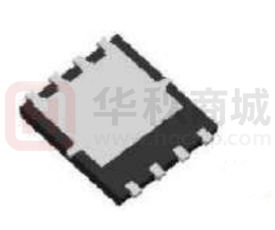
DFN5*6-8
N-Channel
Absolute Maximum Ratings (TA =25ºC unless otherwise noted)
Parameter
Symbol
Drain-Source Voltage
Gate-Source Voltage
Continuous Drain Current
B
TC =100ºC
A
Avalanche Current
Single Pulse Avalanche Energy
C
L =0.3mH
Units
VDS
30
V
VGS
±20
V
ID
A
Pulsed Drain Current
Power Dissipation
TC =25ºC
Maximum
A
TC =25ºC
A
40
IDM
360
A
IS
90
A
EAS
135
mJ
65
W
32
W
TJ, TSTG
-55 to 175
ºC
Symbol
Maximum
Units
PD
TC =100ºC
Junction and Storage Temperature Range
90
Thermal Characteristics
Parameter
Maximum Junction-to-Case
Steady-State
RƟJC
2.3
Maximum Junction-to-Ambient
Steady-State
RƟJA
62
ºC/W
FEB 2019 Version1.0
1/9
www.ascendsemi.com
0755-86970486
�ASDM30N90Q
30V N-Channel MOSFET
Electrical Characteristics(TJ =25ºC unless otherwise noted)
Value
Symbol
Parameter
Conditions
Units
Min
Typ
Max
30
--
--
TJ =25ºC
--
--
1
TJ =125ºC
--
--
25
STATIC PARAMETERS
BVDSS
Drain-Source Breakdown Voltage
ID =250µA,VGS =0V
IDSS
Zero Gate Voltage Drain Current
VDS =30V, VGS =0V
V
μA
IGSS
Gate-Body Leakage Current
VDS =0V, VGS =±20V
--
--
±100
nA
VGS(th)
Gate Threshold Voltage
VDS =VGS, ID =250µA
1
1.6
2.4
V
VGS =10V, ID =30A
--
4.3
5.2
mΩ
RDS(ON)
Static Drain-Source On-Resistance
VGS =4.5V, ID =30A
--
6.9
9.0
mΩ
gFS
Forward Transconductance
VDS =10V, ID =20A
16
--
--
S
VSD
Diode Forward Voltage
IS =30A, VGS =0V
--
--
1
V
IS
Maximum Body-Diode Continuous Current
--
--
90
A
--
2120
--
--
307
--
--
253
--
--
40
--
--
5.4
--
B
DYNAMIC PARAMETERS
Ciss
Input Capacitance
Coss
Output Capacitance
Crss
Reverse Transfer Capacitance
VGS =0V, VDS =15V, f =1MHZ
pF
SWITCHING PARAMETERS
Qg
Total Gate Charge
Qgs
Gate Source Charge
Qgd
Gate Drain Charge
--
9.6
--
tD(on)
Turn-On Delay Time
--
15
--
tr
Turn-On Rise Time
--
32
--
tD(off)
Turn-Off Delay Time
--
15
--
tf
Turn-Off Fall Time
--
12
--
trr
Body Diode Reverse Recovery Time
--
23
--
ns
Qrr
Body Diode Reverse Recovery Charge
--
48
--
nC
VGS =10V,VDS =15V, ID =30A
VGS =10V,VDS =15V, ID =20A,
RG =3Ω
IF =30A, di/dt =100A/μs
nC
ns
A. Single pulse width limited by maximum junction temperature.
B. The maximum current rating is package limited.
C. The power dissipation PD is based on TJ(MAX) =175ºC, using junction-to-case thermal resistance, and is more useful in setting
the upper dissipation limit for cases where additional heatsinking is used.
FEB 2019 Version1.0
2/9
www.ascendsemi.com
0755-86970486
�ASDM30N90Q
30V N-Channel MOSFET
Typical Characteristics TJ = 25ºC, unless otherwise noted
120
80
100
ID (A)
100
ID (A)
120
10V
8V
6V
4.5V
4V
3.5V
60
80
60
40
40
20
20
0
0
1
2
3
4
VDS = 15V
TJ = 125ºC
TJ = 25ºC
0
5
0
1
2
VDS (Volts)
Figure 1: On-Region Characteristics
5
6
10000
9
TJ = 25ºC
Capacitance (pF)
RDS(on) (mΩ)
4
Figure 2: Transfer Characteristics
10
8
7
VGS = 4.5V
6
5
Ciss
1000
Coss
Crss
100
VGS = 10V
4
VGS = 0
f = 1MHz
3
10
2
0
5
10
15
20
25
0
30
ID (A)
Figure 3: On-Resistance vs. Drain Current
5
10
15
20
25
30
VDS (Volts)
Figure 4: Capacitance Characteristics
12
100
10
VDD = 15V
IS (A)
VGS (Volts)
3
VGS (Volts)
8
TJ = 125ºC
10
6
4
TJ = 25ºC
1
2
0
0
10
20
30
40
50
Qg (nC)
Figure 5: Gate Charge Characteristics
FEB 2019 Version1.0
3/9
0.1
0.2
0.4
0.6
0.8
1
VSD (Volts)
Figure 6: Body Diode Forward Voltage
www.ascendsemi.com
0755-86970486
1.2
�ASDM30N90Q
30V N-Channel MOSFET
Typical Characteristics TJ = 25ºC, unless otherwise noted
1.3
Normalized Vgs(th)
Normalized RDS(on)
1.6
VGS = 10V
ID = 30A
1.4
1.2
1.0
0.8
0.6
1.2
ID = 250µA
1.1
1.0
0.9
0.4
0.8
0.2
0.7
0.0
0.6
-50
-25
0
25
50
75
100
125
150
-50
-25
0
Temperature(ºC)
Figure 7: On-Resistance vs. Junction Temperature
50
75
100
125
150
Figure 8: Vgs(th) vs. Junction Temperature
1.15
20
VGS = 0
ID = 250uA
1.10
18
RDS(on) (mΩ)
Normalized BVDSS
25
Temperature(ºC)
1.05
VGS = 10V
ID = 30A
16
14
12
10
1.00
8
TJ = 125ºC
6
0.95
4
2
TJ = 25ºC
0
-50
-25
0
25
50
75
100
125
150
2
TJ, Junction Temperature (ºC)
Figure 9: BVDSS vs. Junction Temperature
4
5
6
7
8
9
10
1000
10
1
RDS(on)
limited
100
10
D = 0.5
D = 0.2
D = 0.1
D = 0.05
D = 0.02
D = 0.01
Single Pulse
0.1
0.01
1E-05
3
VGS, Gate-to-Source Voltage (V)
Figure 10: On-Resistance vs. Gate-Source Voltage
ID (Amps)
Z Ɵ JC Normalized Transient Thermal Resistance
0.90
tp = 10us
tp = 100us
tp = 1ms
tp = 10ms
DC
1
0.1
0.0001
0.001
0.01
0.1
1
Pulse Width (s)
Figure 11: Normalized Transient Thermal Resistance
FEB 2019 Version1.0
4/9
0.1
1
10
100
VDS (Volts)
Figure 12: Safe Operating Area
www.ascendsemi.com
0755-86970486
1000
�ASDM30N90Q
30V N-Channel MOSFET
Figure1:Gate Charge Test Circuit & Waveform
Figure 2: Resistive Switching Test Circuit & Waveforms
Figure 3:Unclamped Inductive Switching Test Circuit & Waveforms
FEB 2019 Version1.0
5/9
www.ascendsemi.com
0755-86970486
�ASDM30N90Q
30V N-Channel MOSFET
Figure 4:Peak Diode Recovery dv/dt Test Circuit & Waveforms (For N-channel)
FEB 2019 Version1.0
6/9
www.ascendsemi.com
0755-86970486
�ASDM30N90Q
30V N-Channel MOSFET
Ordering and Marking Information
Ordering Device No.
Marking
Package
Packing
Quantity
ASDM30N90Q-R
30N90
DFN5*6-8
Tape&Reel
4000/Reel
MARKING
PACKAGE
DFN5*6-8
FEB 2019 Version1.0
30N90
7/9
www.ascendsemi.com
0755-86970486
�ASDM30N90Q
30V N-Channel MOSFET
DFN5*6- 8 PACKAGE IN FORMATION
FEB 2019 Version1.0
8/9
www.ascendsemi.com
0755-86970486
�ASDM30N90Q
30V N-Channel MOSFET
IMPORTANT NOTICE
ShenZhen Ascend Semiconductor incorporated MAKES NO WARRANTY OF ANY KIND, EXPRESS OR IMPLIED, WITH REGARDS TO THIS
DOCUMENT, INCLUDING, BUT NOT LIMITED TO, THE IMPLIED WARRANTIES OF MERCHANTABILITY AND FITNESS FOR A PARTICULAR
PURPOSE (AND THEIR EQUIVALENTS UNDER THE LAWS OF ANY JURISDICTION).
ShenZhen Ascend Semiconductor Incorporated and its subsidiaries reserve the right to make modifications, enhancements, improvements,
corrections or other changes without further notice to this document and any product described herein. ShenZhen Ascend Semiconductor
Incorporated does not assume any liability arising out of the application or use of this document or any product described herein; neither
does ShenZhen Ascend Semiconductor Incorporated convey any license under its patent or trademark rights, nor the rights of others. Any
Customer or user of this document or products described herein in such applications shall assume .
all risks of such use and will agree to hold Ascendsemi Incorporated and all the companies whose products are represented on ShenZhen
Ascend Semiconductor Incorporated website, harmless against all damages.
ShenZhen Ascend Semiconductor Incorporated does not warrant or accept any liability whatsoever in respect of any products purchased
through unauthorized sales channel. Should Customers purchase or use ShenZhen Ascend Semiconductor Incorporated products for any
unintended or unauthorized application, Customers shall indemnify and hold ShenZhen Ascend Semiconductor Incorporated and its
representatives harmless against all claims, damages, expenses, and attorney fees arising out of, directly or indirectly, any claim of personal
injury or death associated with such unintended or unauthorized application.
www.ascendsemi.com
FEB 2019 Version1.0
9/9
www.ascendsemi.com
0755-86970486
�
很抱歉,暂时无法提供与“ASDM30N90Q-R”相匹配的价格&库存,您可以联系我们找货
免费人工找货- 国内价格
- 1+0.82500
- 100+0.77000
- 300+0.71500
- 500+0.66000
- 2000+0.63250
- 5000+0.61600


 工商网监
湘ICP备2023018690号
工商网监
湘ICP备2023018690号
