Application Note: SQ20953
High Efficiency Fast Response, 3A, 30V Input
Synchronous Step Down Regulator
Features
The SQ20953 develops a high efficiency synchronous
step-down DC/DC converter , which is capable of
delivering 3A load current. The SQ20953 operates over
a wide input voltage range from 4.5V to 30V and
integrates main switch and synchronous switch with
very low RDS(ON) to minimize the conduction loss.
• Low RDS(ON) for Internal Switches (Top/Bottom):
110/70 mΩ
• 4.5-30V Input Voltage Range
• Internal Compensation
• Internal 1ms Soft-start Limits the Inrush Current
• Adjustable Switching Frequency Range: 500kHz to
2.5MHz
• 3A Output Current Capability
• 1.5% 0.6V Reference
• Low Quiescent Current
• Cycle-by-cycle Peak Current Limit
• Short Circuit Protection
• Thermal Shutdown and Auto Recovery
• RoHS Compliant and Halogen Free
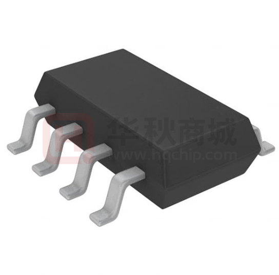
• Compact Package: TSOT23-8
OO
KO
O
General Description
Ordering Information
on
fi
BS
IN
yC
CBS
VIN
dF
Efficiency vs. Load Current
(L=6.8µH/CDRH8D43-6R8)
100
VOUT
L
erg
R1
FB
Sil
EN
LCD-TV
SetTop Box
Notebook
Storage
High Power AP Router
Networking
LX
CIN
ON/
OFF
•
•
•
•
•
•
R2
FS
C1(opt.)
COUT
80
Efficiency (%)
orp
Typical Applications
Note
--
de
nti
a
Package type
TSOT23-8
lP
Applications
.C
Ordering Number
SQ20953AIC
rep
are
The SQ20953 is available in TSOT23-8 package.
or
W
The SQ20953 adopts peak current control scheme. The
switching frequency is adjustable from 500kHz to
2.5MHz using an external resistor. The device also
features ultra low quiescent operating to achieve high
efficiency under light load. The internal soft-start limits
inrush current during power on.
60
40
VIN=9V, VOUT=5V
VIN=12V, VOUT=5V
VIN=24V, VOUT=5V
GND
RFS
20
0
1
10
100
1000
10000
Load Current (mA)
Figure 1. Schematic Diagram
AN_SQ20953 Rev. 0.9
© 2020 Silergy Corp.
Figure 2. Efficiency vs. Load Current
Silergy Corp. Confidential- Prepared for Customer Use Only
1
All Rights Reserved.
�SQ20953
FB
1
8
EN
FS
2
7
BS
GND
3
6
LX
GND
4
5
IN
Top Mark:
Sil
erg
yC
orp
.C
on
fi
de
nti
a
lP
GND
IN
LX
BS
EN
or
W
FS
dF
FB
C5xyz (Device code: C5, x=year code, y=week code, z= lot number code)
Pin Description
Pin Number
Output feedback pin. Connect this pin to the center point of the output resistor
1
divider (as shown in Figure 1) to program the output voltage: V OUT=0.6×(1+R1/R2)
Frequency programming pin. Connect a resistor to ground to program a switching
2
frequency between 500kHz to 2.5MHz. The switching frequency equals to:
fSW=106800/ (RFS+7) kHz, where RFS is in kΩ.
3,4
Ground pin.
5
Input pin. Decouple this pin to the GND pin with at least a 4.7µF ceramic capacitor.
6
Inductor pin. Connect this pin to the switching node of inductor.
7
Boot-strap pin. Supply high side gate driver. Connect a 0.1µF to the LX pin.
8
Enable control. Pull high to turn on. Do not leave it floating.
rep
are
Pin Name
OO
KO
O
Pinout (top view)
AN_SQ20953 Rev. 0.9
© 2020 Silergy Corp.
Silergy Corp. Confidential- Prepared for Customer Use Only
2
All Rights Reserved.
�SQ20953
Block Diagram
IN
HS Current Sense
Internal
Power
Input
UVLO
HS Current Limitation
VCC
OO
KO
O
Comp
BS
HSFET
VCC
EN
LX
Enable
Threshold
PWM Control
&
Protect Logic
HS Current
Sense
Internal
SST
Comp
LSFET
GND
Comp
Error
Amp
Rc
rep
are
VREF
FB
VCC
dF
Slope
Compensation
LS Current Sense
or
W
Internal
clock
FS
SCP
LS current Limitation
OTP
lP
Cc
de
nti
a
Absolute Maximum Ratings (Note 1)
yC
orp
.C
on
fi
IN to GND --------------------------------------------------------------------------------- -------------- -0.3V to 33V
LX, FB, EN, FS to GND------------------------------------------------------------------------------------------ -0.3V to 33V
BS-LX ------------------------------------------------------------------------------------------------------------------- -0.3V to 4V
Dynamic LX voltage in 20ns duration --------------------------------------------------------------------- IN+3V to GND-6V
Power Dissipation, PD @ TA = 25°C TSOT23-8 ---------------------------------------------------------------------------- 2W
Package Thermal Resistance (Note 2)
θ JA --------------------------------------------------------------------------------------------------------------- 60.2°C/W
θ JC --------------------------------------------------------------------------------------------------------------- 11.2°C/W
Junction Temperature Range ------------------------------------------------------------------------------------- -40°C to 150°C
Ambient Temperature Range ------------------------------------------------------------------------------------- -40°C to 105°C
Lead Temperature (Soldering, 10 sec.) ------------------------------------------------------------------------------------ 260°C
Storage Temperature Range -------------------------------------------------------------------------------------- -65°C to 150°C
erg
Recommended Operating Conditions (Note 3)
Sil
Supply Input Voltage ------------------------------------------------------------------------------------------- ------- 4.5V to 30V
Junction Temperature Range ------------------------------------------------------------------------------------- -40°C to 125°C
Ambient Temperature Range -------------------------------------------------------------------------------------- -40°C to 85°C
AN_SQ20953 Rev. 0.9
© 2020 Silergy Corp.
Silergy Corp. Confidential- Prepared for Customer Use Only
3
All Rights Reserved.
�SQ20953
Electrical Characteristics
(VIN = 12V, TJ= -40°C to +125°C. Typical values are at TJ=25°C, unless otherwise specified. The values are
guaranteed by test, design or statistical correlation.)
Test Conditions
Min
4.5
IOUT=0, VFB=VREF×105%
EN=0
TJ=25°C
TJ= -40~125°C
VFB=VCC
VREF
0.591
0.581
-50
or
W
IFB
RDS(ON)1
RDS(ON)2
ILIM,TOP
VENL
VENH
VUVLO
VHYS
Typ
10
1.6
0.6
0.6
110
70
RFS=206.6k
1.5
3.8
V
nA
mΩ
mΩ
A
V
V
V
V
2.5
MHz
500
630
kHz
0.4
1
80
120
2.4
ms
ns
ns
de
nti
a
TSD,HYS
4.5
Unit
V
µA
µA
400
RFS=206.6k
TSD
4.15
0.4
0.5
lP
tSS
rep
are
RFS=35.7k~206.6k
dF
3.8
fOSC
Max
30
27
4
0.609
0.619
50
190
110
6.8
0.5
OO
KO
O
Symbol
VIN
IQ
ISHDN
150
°C
15
°C
on
fi
Parameter
Input Voltage Range
Quiescent Current
Shutdown Current
Feedback Reference
Voltage
FB Input Current
Top FET RON
Bottom FET RON
Top FET Current Limit
EN Input Voltage Low
EN Input Voltage High
Input UVLO Threshold
UVLO Hysteresis
Oscillator Frequency
Program Range
Oscillator Frequency
Accuracy
Soft-start Time
Min ON Time
Min OFF Time
Thermal Shutdown
Temperature
Thermal Shutdown
Hysteresis
θ JA is measured in the natural convection at TA = 25°C on a two-layer Silergy evaluation board.
yC
Note 2:
orp
.C
Note 1: Stresses beyond the “Absolute Maximum Ratings” may cause permanent damage to the device. These are
stress ratings only. Functional operation of the device at these or any other conditions beyond those indicated in the
operational sections of the specification is not implied. Exposure to absolute maximum rating conditions for
extended periods may affect device reliability.
Sil
erg
Note 3: The device is not guaranteed to function outside its operating conditions.
AN_SQ20953 Rev. 0.9
© 2020 Silergy Corp.
Silergy Corp. Confidential- Prepared for Customer Use Only
4
All Rights Reserved.
�SQ20953
Typical Performance Characteristics
(FSW=500kHz, TA = 25°C)
Efficiency vs. Load Current
Load Transient
(L=6.8µH/CDRH8D43-6R8)
(VIN=12V, VOUT=5V, IOUT=0.3A ~ 3A)
100
IL
40
VIN=9V, VOUT=5V
VIN=12V, VOUT=5V
VIN=24V, VOUT=5V
0
1
10
100
1000
10000
Time (40μs/div)
dF
Load Current (mA)
rep
are
Startup from VIN
VLX
10V/div
IL
2V/div
2A/div
on
fi
VOUT
de
nti
a
10V/div
Shutdown from VIN
(VIN=12V, VOUT=5V, IOUT=3A)
VIN
10V/div
VLX
10V/div
VOUT
2V/div
IL
2A/div
lP
(VIN=12V, VOUT=5V, IOUT=3A)
VIN
2A/div
or
W
Efficiency (%)
60
20
0.5V/div
OO
KO
O
ΔVOUT
80
Time (20ms/div)
orp
.C
Time (4ms/div)
Shutdown from Enable
(VIN=12V, VOUT=5V, IOUT=3A)
EN
5V/div
VLX
10V/div
IL
5V/div
VLX
10V/div
2V/div
VOUT
2V/div
2A/div
IL
2A/div
erg
EN
Sil
VOUT
yC
Startup from Enable
(VIN=12V, VOUT=5V, IOUT=3A)
Time (4ms/div)
AN_SQ20953 Rev. 0.9
© 2020 Silergy Corp.
Time (100μs/div)
Silergy Corp. Confidential- Prepared for Customer Use Only
5
All Rights Reserved.
�SQ20953
Short Circuit Protection
Short Circuit Protection
(VIN=12V, VOUT=5V, 0A to Short)
(VIN=12V, VOUT=5V, 3A to Short)
VOUT
5V/div
IL
IL
Time (10ms/div)
dF
Time (10ms/div)
rep
are
Output Ripple
(VIN=12V, VOUT=5V, IOUT= 3A)
VLX
10V/div
IL
de
nti
a
lP
10mV/div
2A/div
or
W
2A/div
ΔVOUT
5V/div
OO
KO
O
VOUT
Sil
erg
yC
orp
.C
Time (2μs/div)
on
fi
2A/div
AN_SQ20953 Rev. 0.9
© 2020 Silergy Corp.
Silergy Corp. Confidential- Prepared for Customer Use Only
6
All Rights Reserved.
�SQ20953
Output Capacitor COUT
The output capacitor is selected to handle the output
ripple noise requirements. Both steady state ripple and
transient requirements must be taken into consideration
when selecting this capacitor. For the best performance,
it is recommended to use X5R or better grade ceramic
capacitor greater than 22µF capacitance.
Operation
OO
KO
O
The SQ20953 develops a high efficiency synchronous
step-down DC/DC converter, which is capable of
delivering 3A load current. The SQ20953 operates over
a wide input voltage range from 4.5V to 30V and
integrates main switch and synchronous switch with
very low RDS(ON) to minimize the conduction loss.
The SQ20953 adopts peak current control scheme. The
switching frequency is adjustable from 500kHz to
2.5MHz using an external resistor. The device also
features ultra low quiescent operating to achieve high
efficiency under light load. The internal soft-start limits
inrush current during power on.
L=
fSW IOUT,MAX 40%
rep
are
where fsw is the switching frequency and IOUT,MAX is
the maximum load current.
The SQ20953 is quite tolerant of different ripple
current amplitude. Consequently, the final choice of
inductance can be slightly off the calculation value
without significantly impacting the performance.
2) The saturation current rating of the inductor must
be selected to be greater than the peak inductor
current under full load conditions.
lP
Because of the high integration in the IC, the
application circuit based on this regulator IC is rather
simple. Only input capacitor CIN, output capacitor COUT,
output inductor L and feedback resistors (R1 and R2)
need to be selected for the targeted applications
specifications.
VOUT (1 − VOUT /VIN,MAX )
dF
Applications Information
or
W
Output Inductor L
There are several considerations in choosing this
inductor.
1) Choose the inductance to provide the desired
ripple current. It is suggested to choose the ripple
current to be about 40% of the maximum output
current. The inductance is calculated as:
0.6V
R1 .
VOUT -0.6V
orp
0.6VFB
yC
R2 =
.C
on
fi
de
nti
a
Feedback Resistor Dividers R1 and R2
Choose R1 and R2 to program the proper output voltage.
To minimize the power consumption under light loads,
it is desirable to choose large resistance values for both
R1 and R2. A value of between 10kΩ and 1MΩ is
highly recommended for both resistors. If VOUT is 3.3V,
R1=100k is chosen, then using following equation, R2
can be calculated to be 22.1k:
GND
VOUT
R1
R2
Sil
erg
Input Capacitor CIN
The ripple current through input capacitor is calculated
as:
ICIN_RMS =IOUT D(1-D)
.
AN_SQ20953 Rev. 0.9
3)
VOUT(1-VOUT/VIN,MAX)
2 fSW L
The DCR of the inductor and the core loss at the
switching frequency must be low enough to
achieve the desired efficiency requirement. It is
desirable to choose an inductor with DCR


 工商网监
湘ICP备2023018690号
工商网监
湘ICP备2023018690号
