OSG80R300FF
Enhancement Mode N-Channel Power MOSFET
General Description
The GreenMOS® high voltage MOSFET utilizes charge balance technology to achieve outstanding
low on-resistance and lower gate charge. It is engineered to minimize conduction loss, provide
superior switching performance and robust avalanche capability.
The GreenMOS® Generic series is optimized for extreme switching performance to minimize
switching loss. It is tailored for high power density applications to meet the highest efficiency
standards.
Features
Low RDS(ON) & FOM
Extremely low switching loss
Excellent stability and uniformity
Applications
PC power
LED lighting
Telecom power
Server power
EV Charger
Solar/UPS
Key Performance Parameters
Parameter
Value
Unit
VDS, min @ Tj(max)
850
V
ID, pulse
45
A
RDS(ON) , max @ VGS=10V
300
mΩ
Qg
23.3
nC
Product Name
Package
Marking
OSG80R300FF
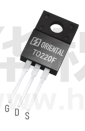
TO220F
OSG80R300F
Marking Information
Package & Pin Information
Oriental Semiconductor © Copyright Reserved V2.0
Page.1
�OSG80R300FF
Enhancement Mode N-Channel Power MOSFET
Absolute Maximum Ratings at Tj=25°C unless otherwise noted
Parameter
Symbol
Value
Unit
Drain-source voltage
VDS
800
V
Gate-source voltage
VGS
±30
V
Continuous drain current1), TC=25 °C
15
ID
A
Continuous drain current1), TC=100 °C
9.5
Pulsed drain current2), TC=25 °C
ID, pulse
45
A
IS
15
A
IS, pulse
45
A
Power dissipation3), TC=25 °C
PD
34
W
Single pulsed avalanche energy5)
EAS
410
mJ
MOSFET dv/dt ruggedness, VDS=0…480 V
dv/dt
50
V/ns
Reverse diode dv/dt, VDS=0…480 V, ISD≤ID
dv/dt
15
V/ns
Tstg, Tj
-55 to 150
°C
Symbol
Value
Unit
Thermal resistance, junction-case
RθJC
3.68
°C/W
Thermal resistance, junction-ambient4)
RθJA
62.5
°C/W
Continuous diode forward current1), TC=25 °C
Diode pulsed current2), TC=25 °C
Operation and storage temperature
Thermal Characteristics
Parameter
Electrical Characteristics at Tj=25°C unless otherwise specified
Parameter
Symbol
Drain-source
breakdown voltage
BVDSS
Gate threshold
voltage
VGS(th)
Drain-source onstate resistance
RDS(ON)
Gate-source
leakage current
IGSS
Drain-source
leakage current
IDSS
Gate resistance
RG
Min.
Typ.
Max.
Unit
VGS=0 V, ID=250 μA
800
V
VGS=0 V, ID=250 μA,
Tj=150 °C
V
VDS=VGS, ID=250 μA
850
2.9
3.9
0.24
0.3
VGS=10 V, ID=7.5 A
Ω
0.64
100
VGS=10 V, ID=7.5 A,
Tj=150 °C
VGS=30 V
nA
-100
Oriental Semiconductor © Copyright Reserved V2.0
Test condition
5
18.2
VGS=-30 V
μA
VDS=800 V, VGS=0 V
Ω
ƒ=1 MHz, Open drain
Page.2
�OSG80R300FF
Enhancement Mode N-Channel Power MOSFET
Dynamic Characteristics
Parameter
Symbol
Min.
Typ.
Max.
Unit
Input capacitance
Ciss
1552
pF
Output capacitance
Coss
80.1
pF
Reverse transfer capacitance
Crss
2.1
pF
Turn-on delay time
td(on)
33.6
ns
tr
20.3
ns
td(off)
57.9
ns
tf
4.5
ns
Rise time
Turn-off delay time
Fall time
Test condition
VGS=0 V,
VDS=50 V,
ƒ=100 kHz
VGS=10 V,
VDS=400 V,
RG=2 Ω,
ID=7.5 A
Gate Charge Characteristics
Parameter
Symbol
Min.
Typ.
Max.
Unit
Total gate charge
Qg
22.7
nC
Gate-source charge
Qgs
8.6
nC
Gate-drain charge
Qgd
2.3
nC
Vplateau
5.5
V
Gate plateau voltage
Test condition
VGS=10 V,
VDS=400 V,
ID=7.5 A
Body Diode Characteristics
Parameter
Symbol
Min.
Typ.
Max.
Unit
1.3
V
Diode forward voltage
VSD
Reverse recovery time
trr
313.7
ns
Reverse recovery charge
Qrr
4.2
μC
Peak reverse recovery current
Irrm
25.2
A
Test condition
IS=15 A,
VGS=0 V
VR=400 V,
IS=7.5 A,
di/dt=100 A/μs
Note
1) Calculated continuous current based on maximum allowable junction temperature.
2) Repetitive rating; pulse width limited by max. junction temperature.
3) Pd is based on max. junction temperature, using junction-case thermal resistance.
4) The value of RθJA is measured with the device mounted on 1 in 2 FR-4 board with 2oz. Copper,
in a still air environment with Ta=25 °C.
5) VDD=100 V, VGS=10 V, L=79.9 mH, starting Tj=25 °C.
Oriental Semiconductor © Copyright Reserved V2.0
Page.3
�OSG80R300FF
Enhancement Mode N-Channel Power MOSFET
Electrical Characteristics Diagrams
4.5
5
12
10 V
6
10
6V
Tj = 25 ℃
10
5.5 V
ID, Drain current(A)
ID, Drain current (A)
1005.5
8
6
4
Tj = 25 ℃
10
1
5V
2
0
VDS= 10 V
VGS= 4.5 V
0
2
4
6
8
0.1
10
2
4
VDS, Drain-source voltage (V)
Figure 1. Typ. output characteristics
8
10
Figure 2. Typ. transfer characteristics
5
10
10
ID = 7.5 A
f = 100 kHz
10
VGS, Gate-source voltage(V)
VGS = 0 V
4
C, Capacitance (pF)
6
VGS, Gate-source voltage(V)
Ciss
3
10
2
10
Coss
1
10
VDS = 400 V
8
6
4
2
Crss
0
10
100
200
300
400
500
600
700
0
800
0
5
Figure 3. Typ. capacitances
20
25
0.70
ID = 250 uA
VGS = 0 V
0.60
RDS(ON), On-resistance(Ω)
BVDSS, Drain-source breakdown voltage (V)
15
Figure 4. Typ. gate charge
1100
1050
10
Qg, Gate charge(nC)
VDS, Drain-source voltage (V)
1000
950
900
850
ID =7.5 A
VGS = 10 V
0.50
0.40
0.30
0.20
800
0.10
750
-50
0
50
100
150
Tj, Junction temperature (℃)
Figure 5. Drain-source breakdown voltage
Oriental Semiconductor © Copyright Reserved V2.0
-50
0
50
100
150
Tj, Junction Temperature (℃)
Figure 6. Drain-source on-state resistance
Page.4
�OSG80R300FF
Enhancement Mode N-Channel Power MOSFET
4.5
1000
Tj = 25 ℃
ID = 250 uA
IS, Source current (A)
Vth, Threshold voltage (V)
4.0
3.5
3.0
100
10
2.5
1
2.0
-50
0
50
100
150
0.5
1.0
1.5
2.0
VSD, Source-Drain voltage (V)
Tj, Junction Temperature (℃)
Figure 7. Threshold voltage
Figure 8. Forward characteristic of body diode
1.0
16
0.8
12
6V
VGS=4.5 V
10 V
6.5 V
0.6
ID, Drain current (A)
RDS(ON), On-resistance(Ω)
14
10
8
6
0.4
4
2
0.2
5
10
15
20
25
30
0
35
0
20
40
Figure 9. Drain-source on-state resistance
100
10 μs
100 μs
1
1 ms
RDS(ON) Limited
10 ms
0.1
DC
0.01
10
100
1000
VDS, Drain-source voltage(V)
Figure 11. Safe operation area TC=25 °C
Oriental Semiconductor © Copyright Reserved V2.0
zthjc Thermal Response(K/W)
ID, Drain current(A)
10
1
80
100
120
140
Figure 10. Drain current
101
0.1
60
TC, Case Temperature (℃)
ID, Drain current(A)
D= tp/T
D= 1
0.5
100
0.2
0.1
0.05
10-1
0.01
0.02
Single Pulse
10-2
10-5
10-4
10-3
10-2
10-1
100
101
102
tp Pulse width(s)
Figure 12. Max. transient thermal impedance
Page.5
�OSG80R300FF
Enhancement Mode N-Channel Power MOSFET
Test circuits and waveforms
Figure 1. Gate charge test circuit & waveform
Figure 2. Switching time test circuit & waveforms
Figure 3. Unclamped inductive switching (UIS) test circuit & waveforms
Figure 4. Diode reverse recovery test circuit & waveforms
Oriental Semiconductor © Copyright Reserved V2.0
Page.6
�OSG80R300FF
Enhancement Mode N-Channel Power MOSFET
Package Information
Symbol
E
A
A1
A4
c
D
H1
e
L
L1
ΦP
ΦP3
F3
G3
b1
b2
Min
9.96
4.50
2.34
2.56
0.40
15.57
12.68
2.88
3.03
3.15
3.15
1.25
1.18
0.70
mm
Nom
10.16
4.70
2.54
2.76
0.50
15.87
6.70REF
2.54BSC
12.98
3.03
3.18
3.45
3.30
1.35
1.28
0.80
Max
10.36
4.90
2.74
2.96
0.65
16.17
13.28
3.18
3.38
3.65
3.45
1.55
1.43
0.95
Version 1: TO220F-C package outline dimension
Oriental Semiconductor © Copyright Reserved V2.0
Page.7
�OSG80R300FF
Enhancement Mode N-Channel Power MOSFET
Package Information
Symbol
A
A1
A2
b
b1
c
D
D1
D2
E
E1
e
e1
H1
L
L1
L2
ΦP
Q
θ1
Min
4.40
1.27
2.30
0.70
1.27
0.45
15.30
9.10
13.10
9.70
7.80
6.30
12.78
3.55
2.73
1˚
mm
Nom
4.50
1.30
2.40
0.50
15.70
9.20
9.90
8.00
2.54BSC
5.08BSC
6.50
13.08
4.60REF
3.60
3˚
Max
4.60
1.33
2.50
0.90
1.40
0.60
16.10
9.30
13.70
10.20
8.20
6.70
13.38
3.50
3.65
2.87
5˚
Version 2: TO220F-J package outline dimension
Oriental Semiconductor © Copyright Reserved V2.0
Page.8
�OSG80R300FF
Enhancement Mode N-Channel Power MOSFET
Ordering Information
Package
Type
Units/
Tube
Tubes/
Inner Box
Units/
Inner Box
Inner Boxes/
Carton Box
Units/
Carton Box
TO220F-C
50
20
1000
6
6000
TO220F-J
50
20
1000
5
5000
Product Information
Product
Package
Pb Free
RoHS
Halogen Free
OSG80R300FF
TO220F
yes
yes
yes
Legal Disclaimer
The information given in this document shall in no event be regarded as a guarantee of
conditions or characteristics. With respect to any examples or hints given herein, any typical
values stated herein and/or any information regarding the application of the device, Oriental
Semiconductor hereby disclaims any and all warranties and liabilities of any kind, including
without limitation, warranties of non-infringement of intellectual property rights of any third
party.
For further information on technology, delivery terms and conditions and prices, please
contact the Oriental Semiconductor sales representatives (www.orientalsemi.com).
© Oriental Semiconductor Co.,Ltd. All Rights Reserved
Oriental Semiconductor © Copyright Reserved V2.0
Page.9
�


 工商网监
湘ICP备2023018690号
工商网监
湘ICP备2023018690号
