HE9073 0.3uA IQ Series
High Speed Low Noise LDO
Features
Low power consumption:0.3uA (Typ.)
High input voltage (up to 7V)
Low voltage drop:
Output voltage accuracy: tolerance ±1%
100mV@100mA@VOUT=3.3V(Typ.)
Build-in Enable/Output Current Limit circuit
High Output Current:≥500mA
Low temperature coefficient
SOT23-5、SOT23-3 、SOT89-3L、
DFN1x1-4L package
Integrated Short-Circuit Protection
Over-Temperature Protection
PSRR=70dB@1KHz
Support Fixed Output Voltage:
1.0v/1.2v/1.5v/1.8v/2.5v/2.8v/3.0v/3.3v
Applications
Battery-powered equipment
Portable games
Communication equipment
Cameras, Video cameras
Mobile phones
Reference voltage sources
General Description
The HE9073 series are highly accurate, low noise,
low ESR ceramic capacitors, reducing cost and
CMOS LDO Voltage Regulators. Offering low
improving output stability. This high level of output
output noise, high ripple rejection ratio, low
stability is maintained even during frequent load
dropout and very fast turn-on times, the HE9073
fluctuations,
series is ideal for today’s cutting edge mobile
response performance and high PSRR achieved
phone. Internally the HE9073 includes a reference
across a broad range of frequencies. The CE
voltage source, error amplifiers, driver transistors,
function allows the output of regulator to be turned
current limiters and phase compensators.
off,
The output voltage is set by current trimming.
consumption.
due
resulting
in
to
the
excellent
greatly
reduced
transient
power
Voltages are selectable in 100mV steps within a
range of 1.2V to 5.0V.
The HE9073 series is also fully compatible with
Order Information
HE9073①②③④⑤
Designator
1
②③
④
⑤
Symbol
A
Integer
D4
P
M
M5
R
G
Description
Standard
Output Voltage(1.2~5.0V)
Package:DFN1x1-4L
Package:SOT89
Package:SOT23-3
Package:SOT23-5
RoHS / Pb Free
Halogen Free
Note:”②③” stands for output voltages. Other voltages can be specially customized
Ver1.1
1
Mar21,2020
�HE9073 0.3uA IQ Series
High Speed Low Noise LDO
Package and Pin assignment
SOT23-5 (Top View)
5
4
Table1: HE9073AXXM5R series (SOT23-5 PKG)
PIN NUMBER
SYMBOL
FUNCTION
1
VIN
Power Input Pin
2
GND
Ground
3
CE
Chip Enable Pin
4
NC
VOUT
No Connection
Mark
1
2
3
5
Output Pin
SOT23-3 (Top View)
2
Table2: HE9073AXXMR series (SOT23-3 PKG)
Mark
1
PIN NUMBER
SYMBOL
FUNCTION
1
GND
Ground
2
VIN
Power Input Pin
3
VOUT
Output Pin
3
SOT89-3 (Top View)
Table3 HE9073AXXPR series (SOT89-3 PKG)
Mark
1
2
3
PIN NO.
PIN NAME
FUNCTION
1
GND
GND pin
2
VIN
Input voltage pin
3
VOUT
Output voltage pin
Table4 HE9073AXXD4R series (DFN1*1-4LPKG)
DFN1x1-4L (Top View)
Ver1.1
PIN NUMBER
SYMBOL
FUNCTION
1
VOUT
Output Pin
2
GND
Ground
3
4
CE
VIN
Chip Enable Pin
Power Input Pin
5
SGND
2
Substrate of Chip.
Leave floating or tie to GND
Mar21,2020
�HE9073 0.3uA IQ Series
High Speed Low Noise LDO
Marking Rule
MARKING
VOLTAGE(V)
MARKING
Package
VOLTAGE(V)
SOT23-3、SOT89-3
Package
SOT23-5、DFN1x1-4L
1.2
AJ12C
1.2
AJ=SA
1.5
AJ15C
1.5
AJ=SE
1.8
AJ18C
1.8
AJ=SH
2.5
AJ25C
2.5
AJ=2E
2.8
AJ28C
2.8
AJ=2H
3.0
AJ30C
3.0
AJ=3B
3.3
AJ33C
3.3
AJ=3C
Absolute Maximum Ratings
Supply Voltage ................................-0.3V to 9V
Storage Temperature ..................-50℃ to 125℃
Operating Temperature .................-40℃ to 85℃
Note: These are stress ratings only. Stresses exceeding the range specified under “Absolute Maximum Ratings”
may cause substantial damage to the device. Functional operation of this device at other conditions beyond
those listed in the specification is not implied and prolonged exposure to extreme conditions may affect
device reliability.
Thermal Information
Symbol
Parameter
θJA
Thermal Resistance (Junction to
Ambient) (Assume no ambient
airflow, no heat sink)
PD
Package
SOT23-3
SOT23-5
SOT89-3
SOT23-3
SOT23-5
Power Dissipation
SOT89-3
Max.
500
Unit
℃/W
500
200
℃/W
℃/W
0.20
0.20
0.50
W
W
W
Note: PD is measured at Ta= 25℃
Ver1.1
3
Mar21,2020
�HE9073 0.3uA IQ Series
High Speed Low Noise LDO
Electrical Characteristics
HE9073 series
(Ta=25℃)
Parameter
Symbol
Output Voltage
Vout
Output Current*1
Iout
Vin-Vout=1V
△Vout1/
4.3V≤Vin≤7V
Line Regulation
Load Regulation
(△Vin·Vout)
△Vout
Output voltage
Temperature
△Vout/(Ta·Vout)
Coefficiency
Conditions
Vin=Vout+1V
1.0mA≤Iout≤30mA
Iout=10mA
Vin= 4.3V
1.0mA≤Iout≤100mA
Iout=30mA
0℃≤Ta≤70℃
Min.
Typ.
Max.
Unit
Vout×0.99
--
Vout×1.01
V
--
500
--
0.05
0.2
%/V
--
10
30
mV
--
±100
--
600
mA
Ppm/
℃
Supply Current
Iss1
--
0.2
0.3
0.5
uA
Input Voltage
Vin
--
--
--
7
V
PSRR
PSRR
--
70
--
dB
F=1KHz,
Vin=4.3Vdc+1Vpp
Typical Application Circuit
Ver1.1
4
Mar21,2020
�HE9073 0.3uA IQ Series
High Speed Low Noise LDO
Typical Performance Characteristics
Test Condition: TA=25°C, unless otherwise note
2、IQ vs VIN (1)
1、VOUT vs TEMP
3、Load Regulation
4、Line Regulation
5、Dropout Voltage vs Load Current
Ver1.1
6、PSRR
5
Mar21,2020
�HE9073 0.3uA IQ Series
High Speed Low Noise LDO
7、Load Transient Response
8、Short Output & Over-Current Response
9、Power-On
10、Power-Off
11、Enable
12、Disable
Note:(1)
Ver1.1
6
Mar21,2020
�HE9073 0.3uA IQ Series
High Speed Low Noise LDO
Operational Explanation
The P-channel MOSFET is connected to the VOUT pin, driven by the subsequent output signal. The output voltage
at the VOUT pin is controlled and stabilized by a system of negative feedback. The IC's internal circuitry can
shut-down by the CE pin's signal
With the HE9073 series, a stable output voltage is achievable even if used with low ESR capacitors as a phase
compensation circuit is built-in. In order to ensure the effectiveness of the phase compensation, we suggest that
an output capacitor (CL) is connected as close as possible to the output pin (VOUT) and the GND pin. Please use
an output capacitor with a capacitance value of at least 10uF. Also, please connect an input capacitor (CIN) of
10uF between the VIN pin and the GND pin in order to ensure a stable power input. Stable phase compensation
may not be ensured if the capacitor runs out capacitance when depending on bias and temperature. In case the
capacitor depends on the bias and temperature, please make sure the capacitor can ensure the actual
capacitance.
The IC's internal circuitry can be shutdown via the signal from the CE pin with the HE9073 series. The operational
logic of the IC's CE pin is selectable (please refer to the selection guide). Although the CE pin is equal to an
inverter input with CMOS hysteresis, with either the pull-up or pull-down options, the CE pin input current will
increase when the IC is in operation. We suggest that you use this IC with either a VIN voltage or a VSS voltage
input at the CE pin. If this IC is used with the correct specifications for the CE pin, the operational logic is fixed and
the IC will operate normally. However, supply current may increase as a result of through current in the IC's
internal circuitry.
Notes on Use
1. Please use this IC within the stated absolute maximum ratings. The IC is liable to malfunction should the
ratings be exceeded.
2. Where wiring impedance is high, operations may become unstable due to noise and/or phase lag depending
on output current. Please keep the resistance low between VIN and VSS wiring in particular.
3. Please wire the input capacitor (CIN) and the output capacitor (CL) as close to the IC as possible.
Ver1.1
7
Mar21,2020
�HE9073 0.3uA IQ Series
High Speed Low Noise LDO
Packaging Information
SOT23-5 Outline Dimensions
Ver1.1
8
Mar21,2020
�HE9073 0.3uA IQ Series
High Speed Low Noise LDO
3-pin SOT23-3 Outline Dimensions
Ver1.1
9
Mar21,2020
�HE9073 0.3uA IQ Series
High Speed Low Noise LDO
Package Information
3-pin SOT89 Outline Dimensions
Ver1.1
10
Mar21,2020
�HE9073 0.3uA IQ Series
High Speed Low Noise LDO
DFN1×1-4 Outline Dimensions
Ver1.1
11
Mar21,2020
�
很抱歉,暂时无法提供与“HE9073A25M5R”相匹配的价格&库存,您可以联系我们找货
免费人工找货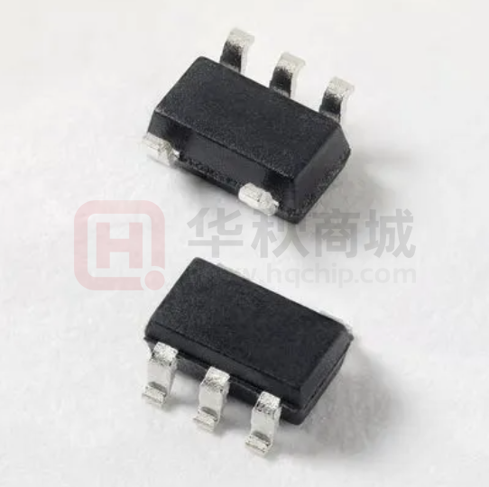


 工商网监
湘ICP备2023018690号
工商网监
湘ICP备2023018690号
