Embedded Multi-Media Card
(e•MMC™ 5.1)
EMMC64G-TY29-5B111
EMMC128-TY29-5B111
EMMC256-TY29-5B111
v1.1
Kingston Digital Inc.
�Product Features
•
•
•
•
•
•
•
Packaged managed NAND flash memory with e•MMC™ 5.1 interface
Backward compatible with all prior e•MMC™ specification revisions
153-ball JEDEC FBGA RoHS Compliant package
Operating voltage range:
o VCCQ = 1.8 V/3.3 V
o VCC = 3.3 V
Operating Temperature - 25C to +85C
Storage Temperature -40C to +85C
Compliant with e•MMC™ 5.1 JEDEC Standard Number JESD84-B51
e•MMC™ Specific Feature Support
• High-speed e•MMC™ protocol
• Variable clock frequencies of 0-200MHz
• Ten-wire bus interface (clock, 1 bit command, 8 bit data bus) with an optional hardware reset
• Supports three different data bus widths: 1 bit(default), 4 bits, 8 bits
• Bus Modes:
o Single data transfer rate: up to 52MB/s (using 8 parallel data lines at 52MHz)
o Dual data rate mode (DDR-104) : up to 104MB/s @ 52MHz
o High speed, single data rate mode (HS-200) : up to 200MB/s @ 200MHz
o High speed, dual data rate mode (HS-400) : up to 400MB/s @ 200MHz
• Supports alternate boot operation mode to provide a simple boot sequence method
o Supports SLEEP/AWAKE (CMD5)
o Host initiated explicit sleep mode for power saving
• Enhanced write protection with permanent and partial protection options
• Multiple user data partition with enhanced attribute for increased reliability
• Error free memory access
o Cyclic Redundancy Code (CRC) for reliable command and data communication
o Internal error correction code (ECC) for improved data storage integrity
o Internal enhanced data management algorithm
o Data protection for sudden power failure during program operations
• Security
o Secure bad block erase commands
o Enhanced write protection with permanent and partial protection options
• Power off notification for sleep
• Field firmware update (FFU)
• Production state awareness
• Device health report
• Command queuing
• Enhanced strobe
• Cache flushing report
• Cache barrier
© Kingston Digital Inc.
Page 2
�•
•
•
•
•
Background operation control & High Priority Interrupt (HPI)
RPMB throughput improvement
Secure write protection
Pre EOL information
Optimal size
Product Description
Kingston’s e•MMC™ products conform to the JEDEC e•MMC™ 5.1 standard. These devices are an
ideal universal storage solution for many commercial and industrial applications. In a single integrated
packaged device, e•MMC™ combines triple-level cell (TLC) NAND flash memory with an onboard
e•MMC™ controller, providing an industry standard interface to the host system. The integrated
e•MMC™ controller directly manages NAND flash media which relieves the host processor of these
tasks, including flash media error control, wear-leveling, NAND flash management and performance
optimization. Future revision to the JEDEC e•MMC™ standard will always maintain backward
compatibility. The industry standard interface to the host processor ensures compatibility across future
NAND flash generations as well, easing product sustainment throughout the product life cycle.
© Kingston Digital Inc.
Page 3
�Configurations
Kingston’s e•MMC™ products support a variety of configurations that allow the e•MMC™ device to be
tailored to your specific application needs. The most popular configurations described below are each
offered under standard part numbers.
Standard TLC – By default the e•MMC™ device is configured with the NAND flash in a standard TLC
mode. This configuration provides reasonable performance and reliability for many applications.
Pseudo Single Level Cell (pSLC) – The TLC NAND flash in the Kingston e•MMC™ device can be
configured to further improve device endurance, data retention, reliability and performance over the
standard TLC configuration. This is done by converting the NAND TLC cells to a pseudo single level cell
(SLC) configuration. In this configuration, along with the performance and reliability gains, the device
capacity is reduced by 2/3 of the capacity. This one-time configuration is achieved by setting the
e•MMC™ enhanced attribute for the hardware partition.
Kingston e•MMC™ can be ordered preconfigured with the option of reliable write or pSLC at no
additional cost. Standard TLC devices can also be one-time configured in-field by following the
procedures outlined in the JEDEC e•MMC™ specification. The JEDEC e•MMC™ specification allows
for many additional configurations such as up to 4 additional general purpose (GPn) hardware partitions
each with the option to support pSLC and reliable write. Additionally, Kingston provides a content
loading service that can streamline your product assembly while reducing production costs. For more
information, contact your Kingston representative.
Kingston e•MMC™ devices are fully compliant with the JEDEC Standard Specification No. JESD84B51. This datasheet provides technical specifications for Kingston’s family of e•MMC™ devices. Refer
to the JEDEC e•MMC™ standard for specific information related to e•MMC™ device function and
operation. See: http://www.jedec.org/sites/default/files/docs/JESD84-B51.pdf
e•MMC™ Mode and Controller
TLC mode using PS8229 - Leading edge 3D NAND flash technology in TLC mode rated to 3,000
endurance cycles.
- Strong data protection with LDPC Error control
- Improved data integrity with end-to-end data protection.
pSLC mode using PS8229 - Leading edge 3D NAND flash technology in pSLC mode rated to 50,000
endurance cycles.
- Strong data protection with LDPC Error control
- Improved data integrity with end-to-end data protection.
© Kingston Digital Inc.
Page 4
�Part Numbering
Figure 1 – Part Number Format
EMMC
64G -
A
xxxx
B
C
-
nnnn
D
Part Number Fields
A: Product Family : EMMC
B: Device Capacity : Available capacities of 64GB – 256GB
C: Hardware Revision and Configuration
D: Device Firmware Revision and Configuration
Table 1 - Device Summary
Product
Part Number
NAND
Density
Package
EMMC64G-TY29-5B111
64GB
FBGA153
EMMC128-TY29-5B111
128GB
FBGA153
EMMC256-TY29-5B111
256GB
FBGA153
Page 5
© Kingston Digital Inc.
Operating
voltage
V CC =3.3V,
V CCQ =1.8V/3.3V
V CC =3.3V,
V CCQ =1.8V/3.3V
V CC =3.3V,
V CCQ =1.8V/3.3V
�Device Performance
Table 2 below provides sequential read and write speeds for all capacities. Performance numbers can vary
under different operating conditions. Values are given at HS400 bus mode. Contact your Kingston
Representative for performance numbers using other bus modes.
Table 2 - Sequential Read / Write Performance
Transfer Rate (MB/s)
Product
Sequential Read
Sequential Write
EMMC64G-TY29-5B111
310
220
EMMC128-TY29-5B111
310
240
EMMC256-TY29-5B111
310
240
Power Consumption
Device current consumption for various device configurations is defined in the power class fields of the
EXT_CSD register. Power consumption values are summarized in Table 3 below.
Table 3 - Device Power Consumption
Read (mA)
Write (mA)
VCCQ = 1.8V
VCC=3.3V
VCCQ = 1.8V
VCC = 3.3V
Standby
(mA)
EMMC64G-TY29-5B111
152.6
93.3
82.3
87.1
0.14
EMMC128-TY29-5B111
151.6
94.2
83.6
89.7
0.15
EMMC256-TY29-5B111
151.7
100.5
83.8
93.6
0.19
Product
Note: Measurement operating conditions were conducted at HS400 bus mode, VCC = 3.3V+5%, VCCQ
= 1.8V+5%. Standby current measured at 8-bit bus, VCC = 3.3V+5%, with clock idle.
© Kingston Digital Inc.
Page 6
�Device and Partition Capacity
The device NAND flash capacity is divided across two boot partitions (4096 KB each), a Replay
Protected Memory Block (RPMB) partition (4096KB), and the main user storage area. Four additional
general purpose storage partitions can be created from the user partition. These partitions can be factory
preconfigured or configured in-field by following the procedure outlined in section 6.2 of the JEDEC
e•MMC™ specification JESD84-B51. A small portion of the NAND storage capacity is used for the
storage of the onboard controller firmware and mapping tables. Additionally, several NAND blocks are
held in reserve to boost performance and extend the life of the e•MMC™ device. Table 4 identifies the
specific capacity of each partition. This information is reported in the device EXT_CSD register. The
contents of this register are also listed in the Appendix.
Table 4 - Partition Capacity
Partition
Part Number
User
Boot 1
Boot 2
RPMB
EMMC64G-TY29-5B111
62,625,153,024 B
4096 KB
4096 KB
4096 KB
EMMC128-TY29-5B111
125,250,306,048 B
4096 KB
4096 KB
4096 KB
EMMC256-TY29-5B111
250,500,612,096 B
4096 KB
4096 KB
4096 KB
Table 5 - e•MMC™ Operating Voltage
Parameter
Supply voltage (NAND)
Max
Unit
3.6
V
3.6
V
Supply voltage (I/O)
V CCQ (1)
1.95
V
Supply power-up for 3.3V
t PRUH
35
ms
Supply power-up for 1.8V
t PRUL
25
ms
Note 1:V CCQ (I/O) 3.3 volt range is not supported while operating in HS200 & HS400 modes
© Kingston Digital Inc.
Symbol
V CC
Page 7
Min
2.7
2.7
1.7
Nom
3.3
3.3
1.8
�e•MMC™ Bus Modes
Kingston e•MMC™ devices support all bus modes defined in the JEDEC e•MMC™ 5.1 specification.
These modes are summarized in Table 6 below.
Table 6 - e•MMC™ Bus Modes
Mode
Data Rate
IO Voltage
Bus Width
CLK
Frequency
Maximum
Data Bus
Throughput
Legacy MMC
Single
3.3V / 1.8V
1, 4, 8
0 – 26 MHz
26 MB/s
High Speed SDR
Single
3.3V / 1.8V
4, 8
0 – 52 MHz
52 MB/s
High Speed DDR
Dual
3.3V / 1.8V
4, 8
0 – 52 MHz
104 MB/s
HS200
Single
1.8V
4, 8
0 – 200 MHz
200 MB/s
HS400
Dual
1.8V
8
0 – 200 MHz
400 MB/s
© Kingston Digital Inc.
Page 8
�Signal Description
Table 7 - e•MMC™ Signals
Name
Type
CLK
I
Clock: Each cycle of this signal directs a one bit transfer on the command
and either a one bit (1x) or a two bits transfer (2x) on all the data lines. The
frequency may vary between zero and the maximum clock frequency.
I/O/PP
Data: These are bidirectional data channels. The DAT signals operate in
push-pull mode. These bidirectional signals are driven by either the
e•MMC™ device or the host controller. By default, after power up or reset,
only DAT0 is used for data transfer. A wider data bus can be configured for
data transfer, using either DAT0-DAT3 or DAT0-DAT7, by the e•MMC™
host controller. The e•MMC™ device includes internal pull-ups for data
lines DAT1-DAT7. Immediately after entering the 4-bit mode, the device
disconnects the internal pull ups of lines DAT1, DAT2, and DAT3.
Correspondingly, immediately after entering to the 8-bit mode, the device
disconnects the internal pull-ups of lines DAT1–DAT7.
I/O/PP/OD
Command: This signal is a bidirectional command channel used for device
initialization and transfer of commands. The CMD signal has two operation
modes: open-drain for initialization mode, and push-pull for fast command
transfer. Commands are sent from the e•MMC™ host controller to the
e•MMC™ device and responses are sent from the device to the host.
DS
O
This signal is generated by the device and used for output in HS400 mode. The
frequency of this signal follows the frequency of CLK. For data output each cycle of
this signal directs two bits transfer(2x) on the data - one bit for positive edge and the
other bit for negative edge. For CRC status response output and CMD response
output (enabled only HS400 enhanced strobe mode), the CRC status and CMD
Response are latched on the positive edge only, and don't care on the negative edge.
RST_n
I
Hardware Reset: By default, hardware reset is disabled and must be enabled in the
EXT_CSD register if used. Otherwise, it can be left un-connected.
RFU
-
Reserved for future use: These pins are not internally connected. Leave floating
NC
-
Not Connected: These pins are not internally connected. Signals can be routed
through these balls to ease printed circuit board design. See Kingston’s Design
Guidelines for further details.
VSF
-
Vendor Specific Function: These pins are not internally connected
Vddi
-
Internal Voltage Node: Note that this is not a power supply input. This pin provides
access to the output of an internal voltage regulator to allow for the connection of an
external Creg capacitor. See Kingston’s Design Guidelines for further details.
Vcc
S
Supply voltage for core
DAT[7:0]
CMD
Description
Note: I=Input; O=Ouput; PP=Push-Pull; OD=Open_Drain; NC=Not Connected(or logical high); S=Power Supply
© Kingston Digital Inc.
Page 9
�Signal Description Continued
Table 8 - e•MMC™ Signals Continued
Name
Type
Description
Vccq
S
Supply voltage for I/O
Vss
S
Supply ground for core
Vssq
S
Supply ground for I/O
Note: I=Input; O=Ouput; PP=Push-Pull; OD=Open_Drain; NC=Not Connected(or logical high); S=Power Supply
Design Guidelines
Design guidelines are outlined in a separate document. Contact your Kingston Representative for more
information.
© Kingston Digital Inc.
Page 10
�Package Dimensions
64GB / 128GB - 11.5 x 13.0 x (Max 0.8mm)
256GB - 11.5 x 13.0 x (Max 1.0mm)
Figure 2 – Package Dimensions
64GB / 128GB
© Kingston Digital Inc.
256GB
Page 11
�Ball Assignment (153 ball)
Table 9 – Ball Assignment, Top View (HS400)
1
2
3
4
5
6
7
8
9
10
11
12
13
14
A
NC
NC
DAT0
DAT1
DAT2
Vss
RFU
NC
NC
NC
NC
NC
NC
NC
A
B
NC
DAT3
DAT4
DAT5
DAT6
DAT7
NC
NC
NC
NC
NC
NC
NC
NC
B
C
NC
Vddi
NC
Vssq
NC
Vccq
NC
NC
NC
NC
NC
NC
NC
NC
C
D
NC
NC
NC
NC
NC
NC
NC
D
E
NC
NC
NC
RFU
VSF
NC
NC
NC
E
F
NC
NC
NC
Vcc
VSF
NC
NC
NC
F
G
NC
NC
RFU
Vss
VSF
NC
NC
NC
G
H
NC
NC
NC
DS
Vss
NC
NC
NC
H
J
NC
NC
NC
Vss
Vcc
NC
NC
NC
J
K
NC
NC
NC
RST_n
VSF
NC
NC
NC
K
L
NC
NC
NC
NC
NC
NC
L
M
NC
NC
NC
Vccq
CMD
CLK
NC
NC
NC
NC
NC
NC
NC
NC
M
N
NC
Vssq
NC
Vccq
Vssq
NC
NC
NC
NC
NC
NC
NC
NC
NC
N
P
NC
NC
Vccq
Vssq
Vccq
Vssq
RFU
NC
NC
RFU
NC
NC
NC
NC
P
1
2
3
4
5
6
7
8
9
10
11
12
13
14
Vcc
RFU
Vss
RFU
VSF
Vss
VSF
Vcc
Note: VSF, RFU and NC balls are not electrically connected. RFU balls may be defined with functionality by the
Joint Electron Device Engineering Council (JEDEC) in future revisions of the e•MMC™ standard. Please refer to
Kingston’s design guidelines for more info.
© Kingston Digital Inc.
Page 12
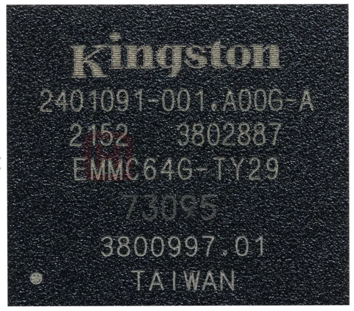
�Device Marking
Figure 4 - EMMC Package Marking
240xxxx-xxx.xxxx-x
YYWW PPPPPPPPPPPP
Part Number
xxxxxxxxxxxx
CoO
Line 1: Kingston logo
Line 2: 240xxxx-xxx.xxxx-x: Internal control number
Line 3: YYWW: Date code (YY– Last 2 digital of year, WW- Work week)
PPPPPPPPPPPP Internal control number (within 12 digits)
Line 4: Part Number: xxxxxx-xxxxxxx
Line 5: xxxxxxxxxxxx: Internal control number (within 12 digits)
Line 6: Country of Origin (CoO): TAIWAN or CHINA
© Kingston Digital Inc.
Page 13
�Card Identification Register (CID)
The Card Identification (CID) register is a 128-bit register that contains device identification information
used during the e•MMC™ protocol device identification phase. Refer to JEDEC Standard Specification
No.JESD84-B51 for details.
Field
MID
reserved
CBX
OID
Bits
[127:120]
[119:114]
[113:112]
[111:104]
PNM
[103:56 ]
PRV
PSN
MDT
CRC
reserved
[ 55:48 ]
[ 47:16 ]
[ 15:8 ]
[ 7:1 ]
[ 0:0 ]
Value
0x70
0x00
0x01
0x00
TY2964 (64GB)
Y29128 (128GB)
Y29256 (256GB)
0x5B
Random
month, year
Follows JEDEC Standard
0x01
A-1
�Card Specific Data Register [CSD]
The Card-Specific Data (CSD) register provides information on how to access the contents stored in
e•MMC™. The CSD registers are used to define the error correction type, maximum data access time, data
transfer speed, data format…etc. For details, refer to section 7.3 of the JEDEC Standard Specification
No.JESD84-B51.
Field
CSD_Structure
SPEC_VER
reserved
TAAC
NSAC
TRAN_SPEED
CCC
READ_BL_LEN
READ_BL_PARTIAL
WRITE_BLK_MISALIGN
READ_BLK_MISALIGN
DSR_IMP
reserved
C_SIZE
VDD_R_CURR_MIN
VDD_R_CURR_MAX
VDD_W_CURR_MIN
VDD_W_CURR_MAX
C_SIZE_MULT
ERASE_GRP_SIZE
ERASE_GRP_MULT
WP_GRP_SIZE
WP_GRP_ENABLE
DEFAULT_ECC
R2W_FACTOR
WRITE_BL_LEN
WRITE_BL_PARTIAL
reserved
CONTENT_PROT_APP
FILE_FORMAT_GRP
COPY
PERM_WRITE_PROTECT
TMP_WRITE_PROTECT
FILE_FORMAT
Bits
[127:126]
[125:122]
[121:120]
[119:112]
[111:104]
[103:96 ]
[ 95:84 ]
[ 83:80 ]
[ 79:79 ]
[ 78:78 ]
[ 77:77 ]
[ 76:76 ]
[ 75:74 ]
[ 73:62 ]
[ 61:59 ]
[ 58:56 ]
[ 55:53 ]
[ 52:50 ]
[ 49:47 ]
[ 46:42 ]
[ 41:37 ]
[ 36:32 ]
[ 31:31 ]
[ 30:29 ]
[ 28:26 ]
[ 25:22 ]
[ 21:21 ]
[ 20:17 ]
[ 16:16 ]
[ 15:15 ]
[ 14:14 ]
[ 13:13 ]
[ 12:12 ]
[ 11:10 ]
B-1
Value
0x03 (V2.0)
0x04 (V4.0~4.2)
0x00
0x4F (40ms)
0x01
0x32 (26Mbit/s)
0x8F5
0x09 (512 Bytes)
0x00
0x00
0x00
0x00
0x00
0xFFF
0x07 (100mA)
0x07 (200mA)
0x07 (100mA)
0x07 (200mA)
0x07 (512 Bytes)
0x1F
0x1F
0x0F
0x01
0x00
0x02
0x09 (512 Bytes)
0x00
0x00
0x00
0x00
0x00
0x00
0x00
0x00
�Field
ECC
CRC
reserved
Bits
[ 9:8 ]
[ 7:1 ]
[ 0:0 ]
B-2
Value
0x00
Follow JEDEC Standard
0x01
�Extended Card Specific Data Register [EXT_CSD]
The Extended CSD register defines the Device properties and selected modes. It is 512 bytes long. The
most significant 320 bytes are the Properties segment, which defines the Device capabilities and cannot
be modified by the host. The lower 192 bytes are the Modes segment, which defines the configuration the
Device is working in. These modes can be changed by the host by means of the SWITCH command. For
details, refer to section 7.4 of the JEDEC Standard Specification No.JESD84-B51.
Field
Reserved
EXT_SECURITY_ERR
S_CMD_SET
HPI_FEATURES
BKOPS_SUPPORT
MAX_PACKED_READS
MAX_PACKED_WRITES
DATA_TAG_SUPPORT
TAG_UNIT_SIZE
TAG_RES_SIZE
CONTEXT_CAPABILITIES
Byte
[511:506]
[505:505]
[504:504]
[503:503]
[502:502]
[501:501]
[500:500]
[499:499]
[498:498]
[497:497]
[496:496]
LARGE_UNIT_SIZE_M1
[495:495]
EXT_SUPPORT
SUPPORTED_MODES
FFU_FEATURES
OPERATION_CODE_TIMEOUT
FFU_ARG
BARRIER_SUPPORT
Reserved
CMDQ_SUPPORT
CMDQ_DEPTH
Reserved
NUMBER_OF_FW_SECTORS_CORRECTLY_PROGRAMMED
VENDOR_PROPRIETARY_HEALTH_REPORT
DEVICE_LIFE_TIME_EST_TYP_B
DEVICE_LIFE_TIME_EST_TYP_A
PRE_EOL_INFO
OPTIMAL_READ_SIZE
OPTIMAL_WRITE_SIZE
OPTIMAL_TRIM_UNIT_SIZE
[494:494]
[493:493]
[492:492]
[491:491]
[490:487]
[486:486]
[485:309]
[308:308]
[307:307]
[306:306]
[305:302]
[301:270]
[269:269]
[268:268]
[267:267]
[266:266]
[265:265]
[264:264]
C-1
Value
0
0x00
0x01
0x01
0x01
0x3C
0x20
0x01
0x03
0x00
0x05
0x53 (64GB)
0xA7 (128GB)
0x4F (256GB)
0x03
0x01
0x00
0x00
65535
0x01
0
0x01
0x0F
0x00
0
0
0x01
0x01
0x01
0x01
0x10
0x01
�Field
DEVICE_VERSION
FIRMWARE_VERSION
PWR_CL_DDR_200_360
CACHE_SIZE
GENERIC_CMD6_TIME
POWER_OFF_LONG_TIME
BKOPS_STATUS
CORRECTLY_PRG_SECTORS_NUM
INI_TIMEOUT_AP
CACHE_FLUSH_POLICY
PWR_CL_DDR_52_360
PWR_CL_DDR_52_195
PWR_CL_200_195
PWR_CL_200_130
MIN_PERF_DDR_W_8_52
MIN_PERF_DDR_R_8_52
Reserved
TRIM_MULT
SEC_FEATURE_SUPPORT
SEC_ERASE_MULT
SEC_TRIM_MULT
BOOT_INFO
Reserved
BOOT_SIZE_MULT
ACC_SIZE
HC_ERASE_GRP_SIZE
Byte
[263:262]
[261:254]
[253:253]
[252:249]
[248:248]
[247:247]
[246:246]
[245:242]
[241:241]
[240:240]
[239:239]
[238:238]
[237:237]
[236:236]
[235:235]
[234:234]
[233:233]
[232:232]
[231:231]
[230:230]
[229:229]
[228:228]
[227:227]
[226:226]
[225:225]
[224:224]
ERASE_TIMEOUT_MULT
[223:223]
REL_WR_SEC_C
HC_WP_GRP_SIZE
S_C_VCC
S_C_VCCQ
PRODUCTION_STATE_AWARENESS_TIMEOUT
S_A_TIMEOUT
SLEEP_NOTIFICATION_TIME
[222:222]
[221:221]
[220:220]
[219:219]
[218:218]
[217:217]
[216:216]
SEC_COUNT
[215:212]
SECURE_WP_INFO
MIN_PERF_W_8_52
MIN_PERF_R_8_52
[211:211]
[210:210]
[209:209]
C-2
Value
0
0x5B
0x00
1536
0x32
0xFF
0x00
0
0x64
0x01
0x00
0x00
0x00
0x00
0x00
0x00
0x00
0x05
0x55
0xF7
0xF7
0x07
0x00
0x20
0x09
0x01
0x11 (64GB/128GB)
0x22 (256GB)
0x01
0x10
0x08
0x08
0x14
0x15
0x0F
122314752 (64GB)
244629504 (128GB)
489259008 (256GB)
0x01
0x08
0x08
�Field
MIN_PERF_W_8_26_4_52
MIN_PERF_R_8_26_4_52
MIN_PERF_W_4_26
MIN_PERF_R_4_26
Reserved
PWR_CL_26_360
PWR_CL_52_360
PWR_CL_26_195
PWR_CL_52_195
PARTITION_SWITCH_TIME
OUT_OF_INTERRUPT_TIME
DRIVER_STRENGTH
DEVICE_TYPE
Reserved
CSD_STRUCTURE
Reserved
EXT_CSD_REV
CMD_SET
Reserved
CMD_SET_REV
Reserved
POWER_CLASS
Reserved
HS_TIMING
STROBE_SUPPORT
BUS_WIDTH
Reserved
ERASED_MEM_CONT
Reserved
PARTITION_CONFIG
BOOT_CONFIG_PROT
BOOT_BUS_CONDITIONS
Reserved
ERASE_GROUP_DEF
BOOT_WP_STATUS
BOOT_WP
Reserved
USER_WP
Reserved
FW_CONFIG
RPMB_SIZE_MULT
C-3
Byte
[208:208]
[207:207]
[206:206]
[205:205]
[204:204]
[203:203]
[202:202]
[201:201]
[200:200]
[199:199]
[198:198]
[197:197]
[196:196]
[195:195]
[194:194]
[193:193]
[192:192]
[191:191]
[190:190]
[189:189]
[188:188]
[187:187]
[186:186]
[185:185]
[184:184]
[183:183]
[182:182]
[181:181]
[180:180]
[179:179]
[178:178]
[177:177]
[176:176]
[175:175]
[174:174]
[173:173]
[172:172]
[171:171]
[170:170]
[169:169]
[168:168]
Value
0x08
0x08
0x08
0x08
0x00
0x00
0x00
0x00
0x00
0xFF
0xFF
0x1F
0x57
0x00
0x02
0x00
0x08
0x00
0x00
0x00
0x00
0x00
0x00
0x01
0x01
0x02
0x00
0x00
0x00
0x00
0x00
0x00
0x00
0x00
0x00
0x00
0x00
0x00
0x00
0x00
0x20
�Field
WR_REL_SET
WR_REL_PARAM
SANITIZE_START
BKOPS_START
BKOPS_EN
RST_n_FUNCTION
HPI_MGMT
PARTITIONING_SUPPORT
Byte
[167:167]
[166:166]
[165:165]
[164:164]
[163:163]
[162:162]
[161:161]
[160:160]
MAX_ENH_SIZE_MULT
[159:157]
PARTITIONS_ATTRIBUTE
PARTITION_SETTING_COMPLETED
GP_SIZE_MULT_4
GP_SIZE_MULT_3
GP_SIZE_MULT_2
GP_SIZE_MULT_1
ENH_SIZE_MULT
ENH_START_ADDR
Reserved
SEC_BAD_BLK_MGMNT
PRODUCTION_STATE_AWARENESS
TCASE_SUPPORT
PERIODIC_WAKEUP
PROGRAM _CID_CSD_DDR_SUPPORT
Reserved
VENDOR_SPECIFIC_FIELD
ERROR_CODE
ERROR_TYPE
NATIVE_SECTOR_SIZE
USE_NATIVE_SECTOR
DATA_SECTOR_SIZE
INI_TIMEOUT_EMU
CLASS_6_CTRL
DYNCAP_NEEDED
EXCEPTION_EVENTS_CTRL
EXCEPTION_EVENTS_STATUS
EXT_PARTITIONS_ATTRIBUTE
CONTEXT_CONF
PACKED_COMMAND_STATUS
PACKED_FAILURE_INDEX
[156:156]
[155:155]
[154:152]
[151:149]
[148:146]
[145:143]
[142:140]
[139:136]
[135:135]
[134:134]
[133:133]
[132:132]
[131:131]
[130:130]
[129:128]
[127:67 ]
[ 66:65 ]
[ 64:64 ]
[ 63:63 ]
[ 62:62 ]
[ 61:61 ]
[ 60:60 ]
[ 59:59 ]
[ 58:58 ]
[ 57:56 ]
[ 55:54 ]
[ 53:52 ]
[ 51:37 ]
[ 36:36 ]
[ 35:35 ]
C-4
Value
0x00
0x15
0x00
0x00
0x00
0x00
0x00
0x07
2488 (64GB)
4977 (128GB)
9954 (256GB)
0x00
0x00
0
0
0
0
0
0
0x00
0x00
0x00
0x00
0x00
0x01
0
N/A
0
0x00
0x00
0x00
0x00
0x00
0x00
0x00
0
0
0
0
0x00
0x00
�Field
POWER_OFF_NOTIFICATION
CACHE_CTRL
FLUSH_CACHE
BARRIER_CTRL
MODE_CONFIG
MODE_OPERATION_CODES
Reserved
FFU_STATUS
PRE_LOADING_DATA_SIZE
Byte
[ 34:34 ]
[ 33:33 ]
[ 32:32 ]
[ 31:31 ]
[ 30:30 ]
[ 29:29 ]
[ 28:27 ]
[ 26:26 ]
[ 25:22 ]
MAX_PRE_LOADING_DATA_SIZE
[ 21:18 ]
PRODUCT_STATE_AWARENESS_ENABLEMENT
SECURE_REMOVAL_TYPE
CMDQ_MODE_EN
Reserved
[ 17:17 ]
[ 16:16 ]
[ 15:15 ]
[ 14:0 ]
C-5
Value
0x00
0x00
0x00
0x00
0x00
0x00
0
0x00
0
40484864 (64GB)
80969728 (128GB)
161939456 (256GB)
0x01
0x09
0x00
0
�History
Revision
History
Date
v1.0
Initial Release
04 / 2022
v1.1
Added Kingston Contact Information
06 / 2023
D-1
�Contact Kingston
For more information, visit us at: https://www.kingston.com/en/solutions/embedded-and-industrial
For direct support, please contact us at: https://www.kingston.com/en/form/embedded
For quick questions, please email us at: emmc@kingston.com
© Kingston Digital Inc.
�


 工商网监
湘ICP备2023018690号
工商网监
湘ICP备2023018690号
