AiP74LVC1G17GB235.TR 数据手册
Wuxi I-CORE Electronics Co., Ltd.
Tab: 835-12
rev:B3
Number:AiP74LVC1G17-AX-LJ-B005EN
or
e
AiP74LVC1G17
Single Buffer Schmitt Trigger
Specification
i-c
Product
Specification Revision History:
Version
Date
Description
2017-07-A1
2021-05-A2
2017-07
2021-05
New
Modify Transfer Characteristics Parameter
2021-09-A3
2021-09
2021-12-A4
2022-03-A5
2021-12
2022-03
Modify ambient temperature to -40℃~+105℃ and add electrical
characteristics of -40℃~+105℃; Modify ordering information
Modify ordering information
Modify ordering information note 1
Address:Building B4,NO.777,Jianzhu Road,Binhu District,Wuxi City,Jiangsu Province
http://www.i-core. cn
P.C.:214072
1/ 12
VER:2022-03-A5
�Wuxi I-CORE Electronics Co., Ltd.
Tab: 835-12
rev:B3
Number:AiP74LVC1G17-AX-LJ-B005EN
1、General Description
The AiP74LVC1G17 provides a buffer function with Schmitt trigger input. It is capable of transforming
slowly changing input signals into sharply defined outputs.
The input can be driven from either 3.3V or 5V devices. This feature allows the use of this device in a
mixed 3.3V and 5V environment.
This device is fully specified for partial power-down applications using IOFF. The IOFF circuitry disables the
output, preventing the damaging backflow current through the device when it is powered down.
or
e
Features:
Wide supply voltage range from 1.65V to 5.5V
±24mA output drive (VCC=3.0V)
CMOS low power consumption
Latch-up performance exceeds 250mA
Direct interface with TTL levels
Unlimited rise and fall times
Input accepts voltages up to 5V
Specified from -40℃ to +105℃
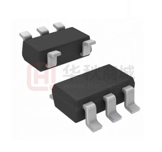
Packaging information: SOT-23-5/SOT-353
Ordering Information:
Reel packing specifications:
Part number
Packaging
form
Marking
code
Reel
quantity
Boxed reel
quantity
SOT-23-5
AFXX
3000
PCS/reel
30000
PCS/box
AiP74LVC1G17GC353.TR
SOT-353
AFXX
3000
PCS/reel
30000
PCS/box
i-c
AiP74LVC1G17GB235.TR
Notes
Dimensions of
plastic enclosure:
2.9mm×1.6mm
Pin spacing:
0.95mm
Dimensions of
plastic enclosure:
2.1mm×1.3mm
Pin spacing:
0.65mm
Note 1: “XX” refers to variable content, meaning year and package batch serial number.
Note 2: If the physical information is inconsistent with the ordering information, please refer to the actual
product.
Address:Building B4,NO.777,Jianzhu Road,Binhu District,Wuxi City,Jiangsu Province
http://www.i-core. cn
P.C.:214072
2/ 12
VER:2022-03-A5
�Wuxi I-CORE Electronics Co., Ltd.
Tab: 835-12
rev:B3
Number:AiP74LVC1G17-AX-LJ-B005EN
2、Block Diagram And Pin Description
2.1、Block Diagram
Figure 1. Logic symbol
e
Figure 2. IEC logic symbol
or
Figure 3. Logic diagram
i-c
2.2、Pin Configurations
2.3、Pin Description
Pin No.
1
2
3
4
5
Pin Name
n.c.
A
GND
Y
VCC
Description
not connected
data input
ground (0V)
data output
supply voltage
2.4、Function Table
Input
A
L
H
Note: H=HIGH voltage level; L=LOW voltage level.
Output
Address:Building B4,NO.777,Jianzhu Road,Binhu District,Wuxi City,Jiangsu Province
http://www.i-core. cn
P.C.:214072
Y
L
H
3/ 12
VER:2022-03-A5
�Wuxi I-CORE Electronics Co., Ltd.
Tab: 835-12
rev:B3
Number:AiP74LVC1G17-AX-LJ-B005EN
3、Electrical Parameter
3.1、Absolute Maximum Ratings
(Voltages are referenced to GND (ground = 0V), unless otherwise specified.)
Symbol
VCC
VI
output voltage
VO
Min.
-0.5
-0.5
-0.5
-0.5
Max.
+6.5
+6.5
VCC+0.5
+6.5
Unit
V
V
V
V
IIK
VI < 0V
-50
-
mA
IOK
VO > VCC or VO < 0V
-
±50
mA
IO
ICC
IGND
VO=0V to VCC
-
-100
±50
+100
-
mA
mA
mA
-
-65
+150
℃
-
-
250
mW
Tstg
Ptot
or
input clamping
current
output clamping
current
output current
supply current
ground current
storage
temperature
total power
dissipation
Soldering
temperature
Conditions
Active mode
Power-down mode; VCC=0V
e
Parameter
supply voltage
input voltage
TL
10s
℃
250
3.2、Recommended Operating Conditions
Symbol
VCC
VI
output voltage
VO
Conditions
Active mode
Power-down mode; VCC=0V
Min.
1.65
0
0
0
Typ.
-
Max.
5.5
5.5
VCC
5.5
Unit
V
V
V
V
-
-40
-
+105
℃
i-c
Parameter
supply voltage
input voltage
ambient
temperature
Tamb
Address:Building B4,NO.777,Jianzhu Road,Binhu District,Wuxi City,Jiangsu Province
http://www.i-core. cn
P.C.:214072
4/ 12
VER:2022-03-A5
�Wuxi I-CORE Electronics Co., Ltd.
Tab: 835-12
rev:B3
Number:AiP74LVC1G17-AX-LJ-B005EN
3.3、Electrical Characteristics
3.3.1、DC Characteristics 1
(Tamb=-40℃ to +85℃, voltages are referenced to GND (ground = 0V), unless otherwise specified.)
HIGH-level
output voltage
LOW-level
output voltage
Symbol
VOH
VOL
Conditions
IO=-100uA;
VCC=1.65V to 5.5V
IO=-4mA; VCC=1.65V
IO=-8mA; VCC=2.3V
VI = VT+ or VTIO=-12mA; VCC=2.7V
IO=-24mA; VCC=3.0V
IO=-32mA; VCC=4.5V
IO=100uA;
VCC=1.65V to 5.5V
IO=4mA; VCC=1.65V
IO=8mA; VCC=2.3V
VI = VT+ or VTIO=12mA; VCC=2.7V
IO=24mA; VCC=3.0V
IO=32mA; VCC=4.5V
Min.
VCC0.1
1.2
1.9
2.2
2.3
3.8
Typ.
Max.
Unit
-
-
V
-
-
V
V
V
V
V
-
-
0.10
V
-
-
0.45
0.30
0.40
0.55
0.55
V
V
V
V
V
e
Parameter
II
VI=5.5V or GND; VCC=0V to 5.5V
-
±0.1
±1
uA
IOFF
VI or VO=5.5V; VCC=0V
-
±0.1
±2
uA
supply current
ICC
-
0.1
4
uA
-
5
500
uA
-
5.0
-
pF
or
input leakage
current
power-off
leakage current
VI=5.5V or GND; IO=0A;
VCC=1.65V to 5.5V
per pin; VI=VCC-0.6V; IO=0A;
VCC=2.3V to 5.5V
i-c
additional
ΔICC
supply current
input
CI
capacitance
Note: All typical values are measured at maximum VCC and Tamb=25℃.
3.3.2、DC Characteristics 2
(Tamb=-40℃ to +105℃, voltages are referenced to GND (ground = 0V), unless otherwise specified.)
Parameter
HIGH-level
output voltage
LOW-level
output voltage
Symbol
VOH
VOL
Conditions
IO=-100uA;
VCC=1.65V to 5.5V
IO=-4mA; VCC=1.65V
IO=-8mA; VCC=2.3V
VI = VT+ or VTIO=-12mA; VCC=2.7V
IO=-24mA; VCC=3.0V
IO=-32mA; VCC=4.5V
IO=100uA;
VCC=1.65V to 5.5V
IO=4mA; VCC=1.65V
IO=8mA; VCC=2.3V
VI = VT+ or VTIO=12mA; VCC=2.7V
IO=24mA; VCC=3.0V
IO=32mA; VCC=4.5V
Address:Building B4,NO.777,Jianzhu Road,Binhu District,Wuxi City,Jiangsu Province
http://www.i-core. cn
P.C.:214072
Min.
VCC0.1
0.95
1.7
1.9
2.0
3.4
Typ.
Max.
Unit
-
-
V
-
-
V
V
V
V
V
-
-
0.10
V
-
-
0.70
0.45
0.60
0.80
0.80
V
V
V
V
V
5/ 12
VER:2022-03-A5
�Wuxi I-CORE Electronics Co., Ltd.
Tab: 835-12
input leakage
current
power-off
leakage current
rev:B3
Number:AiP74LVC1G17-AX-LJ-B005EN
II
VI=5.5V or GND; VCC=0V to 5.5V
-
-
±1
uA
IOFF
VI or VO=5.5V; VCC=0V
-
-
±2
uA
-
-
4
uA
-
-
500
uA
VI=5.5V or GND; IO=0A;
VCC=1.65V to 5.5V
additional
per pin; VI=VCC-0.6V; IO=0A;
ΔICC
supply current
VCC=2.3V to 5.5V
Note: All typical values are measured at maximum VCC and Tamb=25℃.
supply current
ICC
3.3.3、AC Characteristics 1
(Tamb=-40℃ to +85℃, voltages are referenced to GND (ground = 0V), unless otherwise specified.)
Symbol
A to Y
propagation
delay
tpd
Conditions
VCC=1.65V to 1.95V
VCC=2.3V to 2.7V
see Figure 5
VCC=2.7V
VCC=3.0V to 3.6V
VCC=4.5V to 5.5V
Min.
1.0
0.7
0.7
0.7
0.7
Typ.
4.1
2.8
3.2
3.0
2.2
Max.
11.0
6.5
6.5
5.5
5.0
Unit
ns
ns
ns
ns
ns
e
Parameter
i-c
or
Power
dissipation
CPD
VCC=3.3V; VI=GND to VCC
16.6
capacitance
Note:
[1] Typical values are measured at Tamb=25℃ and VCC=1.8V, 2.5V, 2.7V, 3.3V and 5.0V respectively.
[2] tpd is the same as tPLH and tPHL.
[3] CPD is used to determine the dynamic power dissipation (PD in uW).
PD=CPD×VCC2×fi×N+∑(CL×VCC2×fo) where:
fi=input frequency in MHz;
fo=output frequency in MHz;
CL=output load capacitance in pF;
VCC=supply voltage in V;
N=number of inputs switching;
∑(CL×VCC2×fo)=sum of outputs.
pF
3.3.4、AC Characteristics 2
(Tamb=-40℃ to +105℃, voltages are referenced to GND (ground = 0V), unless otherwise specified.)
Parameter
Symbol
A to Y
propagation
delay
tpd
Conditions
VCC=1.65V to 1.95V
VCC=2.3V to 2.7V
see Figure 5
VCC=2.7V
VCC=3.0V to 3.6V
VCC=4.5V to 5.5V
Min.
1.0
0.7
0.7
0.7
0.7
Typ.
-
Max.
14.0
8.5
8.5
7.0
6.5
Unit
ns
ns
ns
ns
ns
Note:
[1] Typical values are measured at Tamb=25℃ and VCC=1.8V, 2.5V, 2.7V, 3.3V and 5.0V respectively.
[2] tpd is the same as tPLH and tPHL.
Address:Building B4,NO.777,Jianzhu Road,Binhu District,Wuxi City,Jiangsu Province
http://www.i-core. cn
P.C.:214072
6/ 12
VER:2022-03-A5
�Wuxi I-CORE Electronics Co., Ltd.
Tab: 835-12
rev:B3
Number:AiP74LVC1G17-AX-LJ-B005EN
3.3.5、Transfer Characteristics 1
(Tamb=-40℃ to +85℃, voltages are referenced to GND (ground = 0V), unless otherwise specified.)
Symbol
positive-going
threshold
voltage
VT+
see Figure 6
and Figure 7
negative-going
threshold
voltage
VT-
see Figure 6
and Figure 7
hysteresis
voltage
VH
see Figure 6,
Figure 7 and
Figure 8
Conditions
VCC=1.8V
VCC=2.3V
VCC=3.0V
VCC=4.5V
VCC=5.5V
VCC=1.8V
VCC=2.3V
VCC=3.0V
VCC=4.5V
VCC=5.5V
VCC=1.8V
VCC=2.3V
VCC=3.0V
VCC=4.5V
VCC=5.5V
Min.
0.82
1.03
1.29
1.84
2.19
0.45
0.64
0.86
1.35
1.61
0.24
0.26
0.27
0.28
0.29
Typ.
1.02
1.25
1.5
2.15
2.6
0.6
0.8
1.1
1.75
2.15
0.4
0.4
0.42
0.45
0.47
Max.
1.2
1.45
1.71
2.41
2.91
0.75
0.96
1.34
2.09
2.59
0.54
0.57
0.64
0.65
0.75
Unit
V
V
V
V
V
V
V
V
V
V
V
V
V
V
V
or
e
Parameter
3.3.6、Transfer Characteristics 2
(Tamb=-40℃ to +105℃, voltages are referenced to GND (ground = 0V), unless otherwise specified.)
Symbol
positive-going
threshold
voltage
VT+
see Figure 6
and Figure 7
Conditions
VCC=1.8V
VCC=2.3V
VCC=3.0V
VCC=4.5V
VCC=5.5V
VCC=1.8V
VCC=2.3V
VCC=3.0V
VCC=4.5V
VCC=5.5V
VCC=1.8V
VCC=2.3V
VCC=3.0V
VCC=4.5V
VCC=5.5V
i-c
Parameter
negative-going
threshold
voltage
VT-
see Figure 6
and Figure 7
hysteresis
voltage
VH
see Figure 6,
Figure 7 and
Figure 8
Address:Building B4,NO.777,Jianzhu Road,Binhu District,Wuxi City,Jiangsu Province
http://www.i-core. cn
P.C.:214072
Min.
0.79
1.00
1.26
1.81
2.16
0.45
0.64
0.86
1.35
1.61
0.17
0.20
0.21
0.22
0.23
Typ.
-
Max.
1.2
1.45
1.71
2.41
2.91
0.78
0.99
1.37
2.12
2.62
0.54
0.57
0.64
0.65
0.75
Unit
V
V
V
V
V
V
V
V
V
V
V
V
V
V
V
7/ 12
VER:2022-03-A5
�Wuxi I-CORE Electronics Co., Ltd.
Tab: 835-12
rev:B3
Number:AiP74LVC1G17-AX-LJ-B005EN
4、Testing Circuit
4.1、AC Testing Circuit
Figure 4. Test circuit for measuring switching times
i-c
or
4.2、AC Testing Waveforms
e
Definitions for test circuit:
RL=Load resistance.
CL=Load capacitance including jig and probe capacitance.
RT=Termination resistance; should be equal to the output impedance Zo of the pulse generator.
VEXT=External voltage for measuring switching times.
Figure 5. The data input (A) to output (Y) propagation delays
4.3、Transfer Characteristics Waveforms
Figure 6. Transfer characteristic
Address:Building B4,NO.777,Jianzhu Road,Binhu District,Wuxi City,Jiangsu Province
http://www.i-core. cn
P.C.:214072
8/ 12
VER:2022-03-A5
�Wuxi I-CORE Electronics Co., Ltd.
Tab: 835-12
rev:B3
Number:AiP74LVC1G17-AX-LJ-B005EN
or
e
Figure 7. Definition of VT+, VT- and VH
Figure 8. Typical transfer characteristics
i-c
4.4、Measurement Points
Supply voltage
VCC
1.65V to 1.95V
2.3V to 2.7V
2.7V
3.0V to 3.6V
4.5V to 5.5V
4.5、Test Data
Supply voltage
VCC
1.65V to 1.95V
2.3V to 2.7V
2.7V
3.0V to 3.6V
4.5V to 5.5V
Input
Output
VM
0.5×VCC
0.5×VCC
1.5V
1.5V
0.5×VCC
VM
0.5×VCC
0.5×VCC
1.5V
1.5V
0.5×VCC
Input
VI
VCC
VCC
2.7V
2.7V
VCC
tr = tf
≤ 2.0ns
≤ 2.0ns
≤ 2.5ns
≤ 2.5ns
≤ 2.5ns
Load
CL
30pF
30pF
50pF
50pF
50pF
Address:Building B4,NO.777,Jianzhu Road,Binhu District,Wuxi City,Jiangsu Province
http://www.i-core. cn
P.C.:214072
VEXT
RL
1kΩ
500Ω
500Ω
500Ω
500Ω
tPLH, tPHL
open
open
open
open
open
9/ 12
VER:2022-03-A5
�Wuxi I-CORE Electronics Co., Ltd.
Tab: 835-12
rev:B3
Number:AiP74LVC1G17-AX-LJ-B005EN
5、Package Information
i-c
or
e
5.1、SOT-23-5
Address:Building B4,NO.777,Jianzhu Road,Binhu District,Wuxi City,Jiangsu Province
http://www.i-core. cn
P.C.:214072
10/ 12
VER:2022-03-A5
�Wuxi I-CORE Electronics Co., Ltd.
Tab: 835-12
rev:B3
Number:AiP74LVC1G17-AX-LJ-B005EN
i-c
or
e
5.2、SOT-353
Address:Building B4,NO.777,Jianzhu Road,Binhu District,Wuxi City,Jiangsu Province
http://www.i-core. cn
P.C.:214072
11/ 12
VER:2022-03-A5
�Wuxi I-CORE Electronics Co., Ltd.
Tab: 835-12
rev:B3
Number:AiP74LVC1G17-AX-LJ-B005EN
6、Statements And Notes
6.1、The name and content of Hazardous substances or Elements in the product
Hazardous substances or Elements
Part name
Lead
and
lead
compo
unds
Mercur
y and
mercur
y
compo
unds
Cadm
ium
and
cadmi
um
comp
ounds
Hexaval
ent
chromiu
m
compoun
ds
Polybro
minated
biphenyl
s
Polybro
minate
d
biphen
yl
ethers
Dibutyl
phthala
te
Butylbe
nzyl
phthala
te
Di-2-et
hylhex
yl
phthala
te
Diisobu
tyl
phthala
te
○
○
○
○
○
○
○
○
○
○
Plastic resin
○
○
○
○
○
○
○
○
○
○
Chip
○
○
○
○
○
○
○
○
○
○
The lead
○
○
○
○
○
○
○
○
○
○
Plastic sheet
installed
○
○
○
e
Lead frame
○
○
○
○
○
○
○
○:Indicates that the content of hazardous substances or elements in the detection limit
of
the following the SJ/T11363-2006 standard.
×:Indicates that the content of hazardous substances or elements exceeding the SJ/T11363-2006
Standard limit requirements.
or
explanation
6.2、Notion
Recommended carefully reading this information before the use of this product;
The information in this document are subject to change without notice;
i-c
This information is using to the reference only, the company is not responsible for any loss;
The company is not responsible for the any infringement of the third party patents or other rights of
the responsibility.
Address:Building B4,NO.777,Jianzhu Road,Binhu District,Wuxi City,Jiangsu Province
http://www.i-core. cn
P.C.:214072
12/ 12
VER:2022-03-A5
�


 工商网监
湘ICP备2023018690号
工商网监
湘ICP备2023018690号
