nRF52805
Product Specification
v1.2
4454_187 v1.2 / 2020-07-02
�Feature list
Features:
•
®
Bluetooth 5.0, 2.4 GHz transceiver
•
•
192 kB flash and 24 kB RAM
•
Advanced on-chip interfaces
•
-97 dBm sensitivity in 1 Mbps Bluetooth Low Energy mode
•
-20 to +4 dBm TX power, configurable in 4 dB steps
•
Programmable peripheral interconnect (PPI)
•
On-air compatible with nRF52, nRF51, nRF24L, and nRF24AP Series
•
10 general purpose I/O pins
•
Supported data rates:
•
EasyDMA automated data transfer between memory and
•
•
®
peripherals
®
•
Bluetooth 5.0 - 2 Mbps, 1 Mbps
•
Proprietary 2.4 GHz – 2 Mbps, 1 Mbps
Single-ended antenna output (on-chip balun)
•
4.6 mA peak current in TX (0 dBm)
•
4.6 mA peak current in RX
•
RSSI (1 dB resolution)
®
®
®
144 EEMBC CoreMark score running from flash memory
•
34.4 µA/MHz running CoreMark from flash memory
•
32.8 µA/MHz running CoreMark from RAM
•
Serial wire debug (SWD)
Nordic SoftDevice ready with support for concurrent multiprotocol
•
Temperature sensor
•
12-bit, 200 ksps ADC – 2 configurable channels with
programmable gain
Arm Cortex -M4 32-bit processor, 64 MHz
•
•
Flexible power management
•
1.7 V to 3.6 V supply voltage range
•
On-chip DC/DC and LDO regulators with automated low current modes
•
Fast wake-up using 64 MHz internal oscillator
•
0.3 µA at 3 V in System OFF mode, no RAM retention
•
0.5 µA at 3 V in System OFF mode with full 24 kB RAM retention
•
1.1 µA at 3 V in System ON mode, with full 24 kB RAM retention, wake on
•
3x 32-bit timer with Counter mode
•
SPI master/slave with EasyDMA
•
I2C compatible two-wire master/slave
•
UART (CTS/RTS) with EasyDMA
•
Quadrature decoder (QDEC)
•
AES HW encryption with EasyDMA
•
2x real-time counter (RTC)
•
Single crystal operation
•
Package variants
•
WLCSP package, 2.482 x 2.464 mm
RTC (running from LFXO clock)
•
1.0 µA at 3 V in System ON mode, no RAM retention, wake on RTC (running
from LFXO clock)
Applications:
•
Proprietary protocol devices
•
Health monitoring
•
Network processor
•
Drug delivery
•
Beacons
•
Asset tags
•
Smart Home sensors
•
Toys
•
Presenters/Stylus
•
Retail tags and labels
4454_187 v1.2
ii
�Contents
Feature list. . . . . . . . . . . . . . . . . . . . . . . . . . . . . . . . . . . . . ii
1
Revision history.
2
About this document.
. . . . . . . . . . . . . . . . . . . . . . . . . . . . . . . .
. . . . . . . . . . . . . . . . . . . . . . . . . . . .
9
10
2.1 Document status . . . . . . . . . . . . . . . . . . . . . . . . . . . . . . . .
2.2 Peripheral chapters . . . . . . . . . . . . . . . . . . . . . . . . . . . . . . .
2.3 Register tables . . . . . . . . . . . . . . . . . . . . . . . . . . . . . . . . .
2.3.1 Fields and values . . . . . . . . . . . . . . . . . . . . . . . . . . . . . .
2.3.2 Permissions . . . . . . . . . . . . . . . . . . . . . . . . . . . . . . . . .
2.4 Registers . . . . . . . . . . . . . . . . . . . . . . . . . . . . . . . . . . . .
2.4.1 DUMMY . . . . . . . . . . . . . . . . . . . . . . . . . . . . . . . . . .
10
10
10
11
11
11
11
3
Block diagram.
13
4
Core components.
5
. . . . . . . . . . . . . . . . . . . . . . . . . . . . . . . .
. . . . . . . . . . . . . . . . . . . . . . . . . . . . . .
14
4.1 CPU . . . . . . . . . . . . . . . . . . . . . . . . . . . . . . . . . . . . . .
4.1.1 Electrical specification . . . . . . . . . . . . . . . . . . . . . . . . . . . .
4.1.2 CPU and support module configuration . . . . . . . . . . . . . . . . . . . . .
4.2 Memory . . . . . . . . . . . . . . . . . . . . . . . . . . . . . . . . . . . .
4.2.1 RAM - Random access memory . . . . . . . . . . . . . . . . . . . . . . . .
4.2.2 Flash - Non-volatile memory . . . . . . . . . . . . . . . . . . . . . . . . .
4.2.3 Memory map . . . . . . . . . . . . . . . . . . . . . . . . . . . . . . . .
4.2.4 Instantiation . . . . . . . . . . . . . . . . . . . . . . . . . . . . . . . .
4.3 NVMC — Non-volatile memory controller . . . . . . . . . . . . . . . . . . . . . .
4.3.1 Writing to flash . . . . . . . . . . . . . . . . . . . . . . . . . . . . . . .
4.3.2 Erasing a page in flash . . . . . . . . . . . . . . . . . . . . . . . . . . . .
4.3.3 Writing to user information configuration registers (UICR) . . . . . . . . . . . . .
4.3.4 Erasing user information configuration registers (UICR) . . . . . . . . . . . . . . .
4.3.5 Erase all . . . . . . . . . . . . . . . . . . . . . . . . . . . . . . . . . .
4.3.6 Partial erase of a page in flash . . . . . . . . . . . . . . . . . . . . . . . . .
4.3.7 Registers . . . . . . . . . . . . . . . . . . . . . . . . . . . . . . . . . .
4.3.8 Electrical specification . . . . . . . . . . . . . . . . . . . . . . . . . . . .
4.4 FICR — Factory information configuration registers . . . . . . . . . . . . . . . . . .
4.4.1 Registers . . . . . . . . . . . . . . . . . . . . . . . . . . . . . . . . . .
4.5 UICR — User information configuration registers . . . . . . . . . . . . . . . . . . .
4.5.1 Registers . . . . . . . . . . . . . . . . . . . . . . . . . . . . . . . . . .
4.6 EasyDMA . . . . . . . . . . . . . . . . . . . . . . . . . . . . . . . . . . .
4.6.1 EasyDMA error handling . . . . . . . . . . . . . . . . . . . . . . . . . . .
4.6.2 EasyDMA array list . . . . . . . . . . . . . . . . . . . . . . . . . . . . . .
4.7 AHB multilayer . . . . . . . . . . . . . . . . . . . . . . . . . . . . . . . . .
4.8 Debug . . . . . . . . . . . . . . . . . . . . . . . . . . . . . . . . . . . . .
4.8.1 DAP - Debug access port . . . . . . . . . . . . . . . . . . . . . . . . . . .
4.8.2 CTRL-AP - Control access port . . . . . . . . . . . . . . . . . . . . . . . . .
4.8.3 Debug interface mode . . . . . . . . . . . . . . . . . . . . . . . . . . . .
4.8.4 Real-time debug . . . . . . . . . . . . . . . . . . . . . . . . . . . . . . .
14
14
14
15
16
16
16
17
18
18
18
19
19
19
19
19
23
23
23
31
31
34
35
36
36
37
38
38
40
40
Power and clock management.
41
. . . . . . . . . . . . . . . . . . . . . . .
5.1 Power management unit (PMU) . . . . . . . . . . . . . . . . . . . . . . . . . . 41
4454_187 v1.2
iii
�6
5.2 Current consumption . . . . . . . . . . . . . . . . . . . . . . . . . . . . . .
5.2.1 Electrical specification . . . . . . . . . . . . . . . . . . . . . . . . . . . .
5.3 POWER — Power supply . . . . . . . . . . . . . . . . . . . . . . . . . . . . .
5.3.1 Regulators . . . . . . . . . . . . . . . . . . . . . . . . . . . . . . . . .
5.3.2 System OFF mode . . . . . . . . . . . . . . . . . . . . . . . . . . . . . .
5.3.3 System ON mode . . . . . . . . . . . . . . . . . . . . . . . . . . . . . .
5.3.4 Power supply supervisor . . . . . . . . . . . . . . . . . . . . . . . . . . .
5.3.5 RAM power control . . . . . . . . . . . . . . . . . . . . . . . . . . . . .
5.3.6 Reset . . . . . . . . . . . . . . . . . . . . . . . . . . . . . . . . . . .
5.3.7 Retained registers . . . . . . . . . . . . . . . . . . . . . . . . . . . . . .
5.3.8 Reset behavior . . . . . . . . . . . . . . . . . . . . . . . . . . . . . . .
5.3.9 Registers . . . . . . . . . . . . . . . . . . . . . . . . . . . . . . . . . .
5.3.10 Electrical specification . . . . . . . . . . . . . . . . . . . . . . . . . . . .
5.4 CLOCK — Clock control . . . . . . . . . . . . . . . . . . . . . . . . . . . . .
5.4.1 HFCLK clock controller . . . . . . . . . . . . . . . . . . . . . . . . . . . .
5.4.2 LFCLK clock controller . . . . . . . . . . . . . . . . . . . . . . . . . . . .
5.4.3 Registers . . . . . . . . . . . . . . . . . . . . . . . . . . . . . . . . . .
5.4.4 Electrical specification . . . . . . . . . . . . . . . . . . . . . . . . . . . .
41
42
46
47
48
49
49
51
51
52
52
53
59
60
61
62
65
71
Peripherals.
73
. . . . . . . . . . . . . . . . . . . . . . . . . . . . . . . . . .
6.1 Peripheral interface . . . . . . . . . . . . . . . . . . . . . . . . . . . . . . .
6.1.1 Peripheral ID . . . . . . . . . . . . . . . . . . . . . . . . . . . . . . . .
6.1.2 Peripherals with shared ID . . . . . . . . . . . . . . . . . . . . . . . . . .
6.1.3 Peripheral registers . . . . . . . . . . . . . . . . . . . . . . . . . . . . .
6.1.4 Bit set and clear . . . . . . . . . . . . . . . . . . . . . . . . . . . . . . .
6.1.5 Tasks . . . . . . . . . . . . . . . . . . . . . . . . . . . . . . . . . . .
6.1.6 Events . . . . . . . . . . . . . . . . . . . . . . . . . . . . . . . . . . .
6.1.7 Shortcuts . . . . . . . . . . . . . . . . . . . . . . . . . . . . . . . . . .
6.1.8 Interrupts . . . . . . . . . . . . . . . . . . . . . . . . . . . . . . . . .
6.2 AAR — Accelerated address resolver . . . . . . . . . . . . . . . . . . . . . . . .
6.2.1 EasyDMA . . . . . . . . . . . . . . . . . . . . . . . . . . . . . . . . . .
6.2.2 Resolving a resolvable address . . . . . . . . . . . . . . . . . . . . . . . . .
6.2.3 Use case example for chaining RADIO packet reception with address resolution using AAR .
6.2.4 IRK data structure . . . . . . . . . . . . . . . . . . . . . . . . . . . . . .
6.2.5 Registers . . . . . . . . . . . . . . . . . . . . . . . . . . . . . . . . . .
6.2.6 Electrical specification . . . . . . . . . . . . . . . . . . . . . . . . . . . .
6.3 BPROT — Block protection . . . . . . . . . . . . . . . . . . . . . . . . . . . .
6.3.1 Registers . . . . . . . . . . . . . . . . . . . . . . . . . . . . . . . . . .
6.4 CCM — AES CCM mode encryption . . . . . . . . . . . . . . . . . . . . . . . .
6.4.1 Keystream generation . . . . . . . . . . . . . . . . . . . . . . . . . . . .
6.4.2 Encryption . . . . . . . . . . . . . . . . . . . . . . . . . . . . . . . . .
6.4.3 Decryption . . . . . . . . . . . . . . . . . . . . . . . . . . . . . . . . .
6.4.4 AES CCM and RADIO concurrent operation . . . . . . . . . . . . . . . . . . . .
6.4.5 Encrypting packets on-the-fly in radio transmit mode . . . . . . . . . . . . . . .
6.4.6 Decrypting packets on-the-fly in RADIO receive mode . . . . . . . . . . . . . . .
6.4.7 CCM data structure . . . . . . . . . . . . . . . . . . . . . . . . . . . . .
6.4.8 EasyDMA and ERROR event . . . . . . . . . . . . . . . . . . . . . . . . . .
6.4.9 Registers . . . . . . . . . . . . . . . . . . . . . . . . . . . . . . . . . .
6.4.10 Electrical specification . . . . . . . . . . . . . . . . . . . . . . . . . . . .
6.5 ECB — AES electronic codebook mode encryption . . . . . . . . . . . . . . . . . .
6.5.1 Shared resources . . . . . . . . . . . . . . . . . . . . . . . . . . . . . .
6.5.2 EasyDMA . . . . . . . . . . . . . . . . . . . . . . . . . . . . . . . . . .
6.5.3 ECB data structure . . . . . . . . . . . . . . . . . . . . . . . . . . . . . .
6.5.4 Registers . . . . . . . . . . . . . . . . . . . . . . . . . . . . . . . . . .
4454_187 v1.2
iv
73
73
74
74
74
74
74
75
75
76
76
76
77
77
77
81
81
83
84
84
85
85
86
86
87
88
89
90
96
96
96
97
97
97
�6.5.5 Electrical specification . . . . . . . . . . . . . . . . . . . . . . . . . . . .
6.6 EGU — Event generator unit . . . . . . . . . . . . . . . . . . . . . . . . . . .
6.6.1 Registers . . . . . . . . . . . . . . . . . . . . . . . . . . . . . . . . .
6.6.2 Electrical specification . . . . . . . . . . . . . . . . . . . . . . . . . . . .
6.7 GPIO — General purpose input/output . . . . . . . . . . . . . . . . . . . . . .
6.7.1 Pin configuration . . . . . . . . . . . . . . . . . . . . . . . . . . . . . .
6.7.2 Registers . . . . . . . . . . . . . . . . . . . . . . . . . . . . . . . . .
6.7.3 Electrical specification . . . . . . . . . . . . . . . . . . . . . . . . . . . .
6.8 GPIOTE — GPIO tasks and events . . . . . . . . . . . . . . . . . . . . . . . . .
6.8.1 Pin events and tasks . . . . . . . . . . . . . . . . . . . . . . . . . . . .
6.8.2 Port event . . . . . . . . . . . . . . . . . . . . . . . . . . . . . . . . .
6.8.3 Tasks and events pin configuration . . . . . . . . . . . . . . . . . . . . . .
6.8.4 Registers . . . . . . . . . . . . . . . . . . . . . . . . . . . . . . . . .
6.8.5 Electrical specification . . . . . . . . . . . . . . . . . . . . . . . . . . . .
6.9 PPI — Programmable peripheral interconnect . . . . . . . . . . . . . . . . . . . .
6.9.1 Pre-programmed channels . . . . . . . . . . . . . . . . . . . . . . . . . .
6.9.2 Registers . . . . . . . . . . . . . . . . . . . . . . . . . . . . . . . . .
6.10 QDEC — Quadrature decoder . . . . . . . . . . . . . . . . . . . . . . . . . .
6.10.1 Sampling and decoding . . . . . . . . . . . . . . . . . . . . . . . . . . .
6.10.2 LED output . . . . . . . . . . . . . . . . . . . . . . . . . . . . . . . .
6.10.3 Debounce filters . . . . . . . . . . . . . . . . . . . . . . . . . . . . .
6.10.4 Accumulators . . . . . . . . . . . . . . . . . . . . . . . . . . . . . . .
6.10.5 Output/input pins . . . . . . . . . . . . . . . . . . . . . . . . . . . . .
6.10.6 Pin configuration . . . . . . . . . . . . . . . . . . . . . . . . . . . . .
6.10.7 Registers . . . . . . . . . . . . . . . . . . . . . . . . . . . . . . . . .
6.10.8 Electrical specification . . . . . . . . . . . . . . . . . . . . . . . . . . .
6.11 RADIO — 2.4 GHz radio . . . . . . . . . . . . . . . . . . . . . . . . . . . .
6.11.1 Packet configuration . . . . . . . . . . . . . . . . . . . . . . . . . . . .
6.11.2 Address configuration . . . . . . . . . . . . . . . . . . . . . . . . . . .
6.11.3 Data whitening . . . . . . . . . . . . . . . . . . . . . . . . . . . . . .
6.11.4 CRC . . . . . . . . . . . . . . . . . . . . . . . . . . . . . . . . . . .
6.11.5 Radio states . . . . . . . . . . . . . . . . . . . . . . . . . . . . . . .
6.11.6 Transmit sequence . . . . . . . . . . . . . . . . . . . . . . . . . . . .
6.11.7 Receive sequence . . . . . . . . . . . . . . . . . . . . . . . . . . . . .
6.11.8 Received signal strength indicator (RSSI) . . . . . . . . . . . . . . . . . . . .
6.11.9 Interframe spacing (IFS) . . . . . . . . . . . . . . . . . . . . . . . . . .
6.11.10 Device address match . . . . . . . . . . . . . . . . . . . . . . . . . . .
6.11.11 Bit counter . . . . . . . . . . . . . . . . . . . . . . . . . . . . . . .
6.11.12 EasyDMA . . . . . . . . . . . . . . . . . . . . . . . . . . . . . . . .
6.11.13 Registers . . . . . . . . . . . . . . . . . . . . . . . . . . . . . . . .
6.11.14 Electrical specification . . . . . . . . . . . . . . . . . . . . . . . . . . .
6.12 RNG — Random number generator . . . . . . . . . . . . . . . . . . . . . . .
6.12.1 Bias correction . . . . . . . . . . . . . . . . . . . . . . . . . . . . . .
6.12.2 Speed . . . . . . . . . . . . . . . . . . . . . . . . . . . . . . . . . .
6.12.3 Registers . . . . . . . . . . . . . . . . . . . . . . . . . . . . . . . . .
6.12.4 Electrical specification . . . . . . . . . . . . . . . . . . . . . . . . . . .
6.13 RTC — Real-time counter . . . . . . . . . . . . . . . . . . . . . . . . . . .
6.13.1 Clock source . . . . . . . . . . . . . . . . . . . . . . . . . . . . . . .
6.13.2 Resolution versus overflow and the PRESCALER . . . . . . . . . . . . . . . . .
6.13.3 COUNTER register . . . . . . . . . . . . . . . . . . . . . . . . . . . . .
6.13.4 Overflow features . . . . . . . . . . . . . . . . . . . . . . . . . . . . .
6.13.5 TICK event . . . . . . . . . . . . . . . . . . . . . . . . . . . . . . . .
6.13.6 Event control feature . . . . . . . . . . . . . . . . . . . . . . . . . . .
6.13.7 Compare feature . . . . . . . . . . . . . . . . . . . . . . . . . . . . .
4454_187 v1.2
v
100
100
100
102
102
103
105
110
110
111
111
112
112
116
116
118
118
122
123
124
124
124
125
125
126
137
137
137
138
139
139
140
141
142
144
144
145
145
146
147
168
173
173
173
174
176
176
177
177
178
178
178
179
179
�6.13.8 TASK and EVENT jitter/delay . . . . . . . . . . . . . . . . . . . . . . . . .
6.13.9 Reading the COUNTER register . . . . . . . . . . . . . . . . . . . . . . .
6.13.10 Registers . . . . . . . . . . . . . . . . . . . . . . . . . . . . . . . .
6.13.11 Electrical specification . . . . . . . . . . . . . . . . . . . . . . . . . . .
6.14 SAADC — Successive approximation analog-to-digital converter . . . . . . . . . . . .
6.14.1 Overview . . . . . . . . . . . . . . . . . . . . . . . . . . . . . . . .
6.14.2 Digital output . . . . . . . . . . . . . . . . . . . . . . . . . . . . . . .
6.14.3 Analog inputs and channels . . . . . . . . . . . . . . . . . . . . . . . . .
6.14.4 Operation modes . . . . . . . . . . . . . . . . . . . . . . . . . . . . .
6.14.5 EasyDMA . . . . . . . . . . . . . . . . . . . . . . . . . . . . . . . . .
6.14.6 Resistor ladder . . . . . . . . . . . . . . . . . . . . . . . . . . . . . .
6.14.7 Reference . . . . . . . . . . . . . . . . . . . . . . . . . . . . . . . .
6.14.8 Acquisition time . . . . . . . . . . . . . . . . . . . . . . . . . . . . . .
6.14.9 Limits event monitoring . . . . . . . . . . . . . . . . . . . . . . . . . .
6.14.10 Registers . . . . . . . . . . . . . . . . . . . . . . . . . . . . . . . .
6.14.11 Electrical specification . . . . . . . . . . . . . . . . . . . . . . . . . . .
6.14.12 Performance factors . . . . . . . . . . . . . . . . . . . . . . . . . . .
6.15 SPI — Serial peripheral interface master . . . . . . . . . . . . . . . . . . . . .
6.15.1 Functional description . . . . . . . . . . . . . . . . . . . . . . . . . . .
6.15.2 Registers . . . . . . . . . . . . . . . . . . . . . . . . . . . . . . . . .
6.15.3 Electrical specification . . . . . . . . . . . . . . . . . . . . . . . . . . .
6.16 SPIM — Serial peripheral interface master with EasyDMA . . . . . . . . . . . . . .
6.16.1 SPI master transaction sequence . . . . . . . . . . . . . . . . . . . . . . .
6.16.2 Master mode pin configuration . . . . . . . . . . . . . . . . . . . . . . .
6.16.3 EasyDMA . . . . . . . . . . . . . . . . . . . . . . . . . . . . . . . . .
6.16.4 Low power . . . . . . . . . . . . . . . . . . . . . . . . . . . . . . . .
6.16.5 Registers . . . . . . . . . . . . . . . . . . . . . . . . . . . . . . . . .
6.16.6 Electrical specification . . . . . . . . . . . . . . . . . . . . . . . . . . .
6.17 SPIS — Serial peripheral interface slave with EasyDMA . . . . . . . . . . . . . . . .
6.17.1 Shared resources . . . . . . . . . . . . . . . . . . . . . . . . . . . . .
6.17.2 EasyDMA . . . . . . . . . . . . . . . . . . . . . . . . . . . . . . . . .
6.17.3 SPI slave operation . . . . . . . . . . . . . . . . . . . . . . . . . . . .
6.17.4 Pin configuration . . . . . . . . . . . . . . . . . . . . . . . . . . . . .
6.17.5 Registers . . . . . . . . . . . . . . . . . . . . . . . . . . . . . . . . .
6.17.6 Electrical specification . . . . . . . . . . . . . . . . . . . . . . . . . . .
6.18 SWI — Software interrupts . . . . . . . . . . . . . . . . . . . . . . . . . . .
6.18.1 Registers . . . . . . . . . . . . . . . . . . . . . . . . . . . . . . . . .
6.19 TEMP — Temperature sensor . . . . . . . . . . . . . . . . . . . . . . . . . .
6.19.1 Registers . . . . . . . . . . . . . . . . . . . . . . . . . . . . . . . . .
6.19.2 Electrical specification . . . . . . . . . . . . . . . . . . . . . . . . . . .
6.20 TWI — I2C compatible two-wire interface . . . . . . . . . . . . . . . . . . . . .
6.20.1 Functional description . . . . . . . . . . . . . . . . . . . . . . . . . . .
6.20.2 Master mode pin configuration . . . . . . . . . . . . . . . . . . . . . . .
6.20.3 Shared resources . . . . . . . . . . . . . . . . . . . . . . . . . . . . .
6.20.4 Master write sequence . . . . . . . . . . . . . . . . . . . . . . . . . . .
6.20.5 Master read sequence . . . . . . . . . . . . . . . . . . . . . . . . . . .
6.20.6 Master repeated start sequence . . . . . . . . . . . . . . . . . . . . . . .
6.20.7 Low power . . . . . . . . . . . . . . . . . . . . . . . . . . . . . . . .
6.20.8 Registers . . . . . . . . . . . . . . . . . . . . . . . . . . . . . . . . .
6.20.9 Electrical specification . . . . . . . . . . . . . . . . . . . . . . . . . . .
6.21 TIMER — Timer/counter . . . . . . . . . . . . . . . . . . . . . . . . . . . .
6.21.1 Capture . . . . . . . . . . . . . . . . . . . . . . . . . . . . . . . . .
6.21.2 Compare . . . . . . . . . . . . . . . . . . . . . . . . . . . . . . . . .
6.21.3 Task delays . . . . . . . . . . . . . . . . . . . . . . . . . . . . . . . .
4454_187 v1.2
vi
181
183
184
189
189
189
190
191
191
193
194
195
195
196
197
211
212
212
213
216
219
220
221
222
223
223
223
232
233
234
234
234
236
237
247
249
249
249
250
256
256
256
257
257
258
258
259
260
260
268
269
270
270
270
�6.21.4 Task priority . . . . . . . . . . . . . . . . . . . . . . . . . . . . . . .
6.21.5 Registers . . . . . . . . . . . . . . . . . . . . . . . . . . . . . . . . .
6.21.6 Electrical specification . . . . . . . . . . . . . . . . . . . . . . . . . . .
6.22 TWIM — I2C compatible two-wire interface master with EasyDMA . . . . . . . . . . .
6.22.1 EasyDMA . . . . . . . . . . . . . . . . . . . . . . . . . . . . . . . . .
6.22.2 Master write sequence . . . . . . . . . . . . . . . . . . . . . . . . . . .
6.22.3 Master read sequence . . . . . . . . . . . . . . . . . . . . . . . . . . .
6.22.4 Master repeated start sequence . . . . . . . . . . . . . . . . . . . . . . .
6.22.5 Low power . . . . . . . . . . . . . . . . . . . . . . . . . . . . . . . .
6.22.6 Master mode pin configuration . . . . . . . . . . . . . . . . . . . . . . .
6.22.7 Registers . . . . . . . . . . . . . . . . . . . . . . . . . . . . . . . . .
6.22.8 Electrical specification . . . . . . . . . . . . . . . . . . . . . . . . . . .
6.22.9 Pullup resistor . . . . . . . . . . . . . . . . . . . . . . . . . . . . . .
6.23 TWIS — I2C compatible two-wire interface slave with EasyDMA . . . . . . . . . . . .
6.23.1 EasyDMA . . . . . . . . . . . . . . . . . . . . . . . . . . . . . . . . .
6.23.2 TWI slave responding to a read command . . . . . . . . . . . . . . . . . . .
6.23.3 TWI slave responding to a write command . . . . . . . . . . . . . . . . . . .
6.23.4 Master repeated start sequence . . . . . . . . . . . . . . . . . . . . . . .
6.23.5 Terminating an ongoing TWI transaction . . . . . . . . . . . . . . . . . . . .
6.23.6 Low power . . . . . . . . . . . . . . . . . . . . . . . . . . . . . . . .
6.23.7 Slave mode pin configuration . . . . . . . . . . . . . . . . . . . . . . . .
6.23.8 Registers . . . . . . . . . . . . . . . . . . . . . . . . . . . . . . . . .
6.23.9 Electrical specification . . . . . . . . . . . . . . . . . . . . . . . . . . .
6.24 UART — Universal asynchronous receiver/transmitter . . . . . . . . . . . . . . . .
6.24.1 Functional description . . . . . . . . . . . . . . . . . . . . . . . . . . .
6.24.2 Pin configuration . . . . . . . . . . . . . . . . . . . . . . . . . . . . .
6.24.3 Shared resources . . . . . . . . . . . . . . . . . . . . . . . . . . . . .
6.24.4 Transmission . . . . . . . . . . . . . . . . . . . . . . . . . . . . . . .
6.24.5 Reception . . . . . . . . . . . . . . . . . . . . . . . . . . . . . . . .
6.24.6 Suspending the UART . . . . . . . . . . . . . . . . . . . . . . . . . . .
6.24.7 Error conditions . . . . . . . . . . . . . . . . . . . . . . . . . . . . . .
6.24.8 Using the UART without flow control . . . . . . . . . . . . . . . . . . . . .
6.24.9 Parity and stop bit configuration . . . . . . . . . . . . . . . . . . . . . . .
6.24.10 Registers . . . . . . . . . . . . . . . . . . . . . . . . . . . . . . . .
6.24.11 Electrical specification . . . . . . . . . . . . . . . . . . . . . . . . . . .
6.25 UARTE — Universal asynchronous receiver/transmitter with EasyDMA . . . . . . . . .
6.25.1 EasyDMA . . . . . . . . . . . . . . . . . . . . . . . . . . . . . . . . .
6.25.2 Transmission . . . . . . . . . . . . . . . . . . . . . . . . . . . . . . .
6.25.3 Reception . . . . . . . . . . . . . . . . . . . . . . . . . . . . . . . .
6.25.4 Error conditions . . . . . . . . . . . . . . . . . . . . . . . . . . . . . .
6.25.5 Using the UARTE without flow control . . . . . . . . . . . . . . . . . . . .
6.25.6 Parity and stop bit configuration . . . . . . . . . . . . . . . . . . . . . . .
6.25.7 Low power . . . . . . . . . . . . . . . . . . . . . . . . . . . . . . . .
6.25.8 Pin configuration . . . . . . . . . . . . . . . . . . . . . . . . . . . . .
6.25.9 Registers . . . . . . . . . . . . . . . . . . . . . . . . . . . . . . . . .
6.25.10 Electrical specification . . . . . . . . . . . . . . . . . . . . . . . . . . .
6.26 WDT — Watchdog timer . . . . . . . . . . . . . . . . . . . . . . . . . . . .
6.26.1 Reload criteria . . . . . . . . . . . . . . . . . . . . . . . . . . . . . .
6.26.2 Temporarily pausing the watchdog . . . . . . . . . . . . . . . . . . . . . .
6.26.3 Watchdog reset . . . . . . . . . . . . . . . . . . . . . . . . . . . . . .
6.26.4 Registers . . . . . . . . . . . . . . . . . . . . . . . . . . . . . . . . .
6.26.5 Electrical specification . . . . . . . . . . . . . . . . . . . . . . . . . . .
7
Hardware and layout.
4454_187 v1.2
. . . . . . . . . . . . . . . . . . . . . . . . . . . .
vii
270
270
275
275
277
277
278
279
280
280
280
291
292
292
294
294
296
297
297
298
298
298
308
309
309
309
310
310
311
311
312
312
312
312
321
321
322
322
323
324
324
325
325
325
325
338
338
339
339
339
339
342
343
�7.1 Pin assignments . . . . . . . . . . . . . . . . . . . . . . . . . . . . . . . .
7.1.1 WLCSP ball assignments . . . . . . . . . . . . . . . . . . . . . . . . . . .
7.2 Mechanical specifications . . . . . . . . . . . . . . . . . . . . . . . . . . . .
7.2.1 WLCSP 2.482 x 2.464 mm package . . . . . . . . . . . . . . . . . . . . . .
7.3 Reference circuitry . . . . . . . . . . . . . . . . . . . . . . . . . . . . . . .
7.3.1 Schematic CAAA WLCSP with internal LDO regulator setup . . . . . . . . . . . . .
7.3.2 Schematic CAAA WLCSP with DC/DC regulator setup . . . . . . . . . . . . . . .
7.3.3 PCB guidelines . . . . . . . . . . . . . . . . . . . . . . . . . . . . . . .
7.3.4 PCB layout example . . . . . . . . . . . . . . . . . . . . . . . . . . . . .
8
9
Recommended operating conditions.
343
343
344
345
345
345
346
348
348
. . . . . . . . . . . . . . . . . . .
351
8.1 WLCSP light sensitivity . . . . . . . . . . . . . . . . . . . . . . . . . . . . .
351
Absolute maximum ratings.
10 Ordering information.
10.1
10.2
10.3
10.4
10.5
. . . . . . . . . . . . . . . . . . . . . . . .
352
. . . . . . . . . . . . . . . . . . . . . . . . . . .
353
IC marking . . . . . . . . . . . . . . . . . . . . . . . . . . . . . . . . . .
Box labels . . . . . . . . . . . . . . . . . . . . . . . . . . . . . . . . . .
Order code . . . . . . . . . . . . . . . . . . . . . . . . . . . . . . . . .
Code ranges and values . . . . . . . . . . . . . . . . . . . . . . . . . . . .
Product options . . . . . . . . . . . . . . . . . . . . . . . . . . . . . . .
11 Legal notices.
4454_187 v1.2
. . . . . . . . . . . . . . . . . . . . . . . . . . . . . . . .
viii
353
353
354
355
356
358
�1
Revision history
Date
Version
Description
July 2020
1.2
The following content has been added or updated:
• Added QDEC — Quadrature decoder on page 122
peripheral information.
June 2020
1.1
The following content has been added or updated:
• About this document on page 10 - Added field
permission descriptions section.
• Current consumption on page 41 - Parameter update,
modified graphs.
• Corrected minimum valid value for EasyDMA MAXCNT and
AMOUNT registers in SPIM — Serial peripheral interface
master with EasyDMA on page 220, SPIS — Serial
peripheral interface slave with EasyDMA on page 233,
TWIM — I2C compatible two-wire interface master with
EasyDMA on page 275, TWIS — I2C compatible twowire interface slave with EasyDMA on page 292 and
UARTE — Universal asynchronous receiver/transmitter
with EasyDMA on page 321.
• RADIO — 2.4 GHz radio on page 137 - EDSAMPLE
register corrected to read-only. Output power and
sensitivity figures changed. Parameters C/I2MBLE,
+2MHz,-2MHz,+4MHz,-4MHz updated. All Radio Timing
parameters set as Typical.
• SPIS — Serial peripheral interface slave with EasyDMA on
page 233 - Relaxed parameter tSPIS,HCSN.
• TWIM — I2C compatible two-wire interface master with
EasyDMA on page 275 - Parameter tTWIM,HD_STA value
updated.
• Editorial changes
August 2019
4454_187 v1.2
1.0
First release
9
�2
About this document
This document is organized into chapters that are based on the modules and peripherals available in the
IC.
2.1 Document status
The document status reflects the level of maturity of the document.
Document name
Description
Objective Product Specification (OPS)
Applies to document versions up to 1.0.
This document contains target specifications for
product development.
Product Specification (PS)
Applies to document versions 1.0 and higher.
This document contains final product
specifications. Nordic Semiconductor ASA reserves
the right to make changes at any time without
notice in order to improve design and supply the
best possible product.
Table 1: Defined document names
2.2 Peripheral chapters
Every peripheral has a unique capitalized name or an abbreviation of its name, e.g. TIMER, used for
identification and reference. This name is used in chapter headings and references, and it will appear in
the ARM® Cortex® Microcontroller Software Interface Standard (CMSIS) hardware abstraction layer to
identify the peripheral.
The peripheral instance name, which is different from the peripheral name, is constructed using the
peripheral name followed by a numbered postfix, starting with 0, for example, TIMER0. A postfix is
normally only used if a peripheral can be instantiated more than once. The peripheral instance name is
also used in the CMSIS to identify the peripheral instance.
The chapters describing peripherals may include the following information:
• A detailed functional description of the peripheral
• Register configuration for the peripheral
• Electrical specification tables, containing performance data which apply for the operating conditions
described in Recommended operating conditions on page 351.
2.3 Register tables
Individual registers are described using register tables. These tables are built up of two sections. The first
three colored rows describe the position and size of the different fields in the register. The following rows
describe the fields in more detail.
4454_187 v1.2
10
�About this document
2.3.1 Fields and values
The Id (Field Id) row specifies the bits that belong to the different fields in the register. If a field has
enumerated values, then every value will be identified with a unique value id in the Value Id column.
A blank space means that the field is reserved and read as undefined, and it also must be written as 0
to secure forward compatibility. If a register is divided into more than one field, a unique field name is
specified for each field in the Field column. The Value Id may be omitted in the single-bit bit fields when
values can be substituted with a Boolean type enumerator range, e.g. true/false, disable(d)/enable(d), on/
off, and so on.
Values are usually provided as decimal or hexadecimal. Hexadecimal values have a 0x prefix, decimal
values have no prefix.
The Value column can be populated in the following ways:
• Individual enumerated values, for example 1, 3, 9.
• Range of values, e.g. [0..4], indicating all values from and including 0 and 4.
• Implicit values. If no values are indicated in the Value column, all bit combinations are supported, or
alternatively the field's translation and limitations are described in the text instead.
If two or more fields are closely related, the Value Id, Value, and Description may be omitted for all but
the first field. Subsequent fields will indicate inheritance with '..'.
A feature marked Deprecated should not be used for new designs.
2.3.2 Permissions
Different fields in a register might have different access permissions enforced by hardware.
The access permission for each register field is documented in the Access column in the following ways:
Access
Description
Hardware behavior
RO
Read-only
Field can only be read. A write will be ignored.
WO
Write-only
Field can only be written. A read will return an undefined value.
RW
Read-write
Field can be read and written multiple times.
W1
Write-once
Field can only be written once per reset. Any subsequent write will be ignored. A read will return an undefined value.
RW1
Read-write-once
Field can be read multiple times, but only written once per reset. Any subsequent write will be ignored.
Table 2: Register field permission schemes
2.4 Registers
Register
Offset
Description
DUMMY
0x514
Example of a register controlling a dummy feature
Table 3: Register overview
2.4.1 DUMMY
Address offset: 0x514
Example of a register controlling a dummy feature
4454_187 v1.2
11
�About this document
Bit number
31 30 29 28 27 26 25 24 23 22 21 20 19 18 17 16 15 14 13 12 11 10 9 8 7 6 5 4 3 2 1 0
ID
D D D D
Reset 0x00050002
ID
Access
Field
A
RW FIELD_A
C C C
B
A A
0 0 0 0 0 0 0 0 0 0 0 0 0 1 0 1 0 0 0 0 0 0 0 0 0 0 0 0 0 0 1 0
Value ID
Value
Description
Example of a read-write field with several enumerated
values
Disabled
0
The example feature is disabled
NormalMode
1
The example feature is enabled in normal mode
ExtendedMode
2
The example feature is enabled along with extra
functionality
B
RW FIELD_B
C
RW FIELD_C
D
RW FIELD_D
Example of a deprecated read-write field
Disabled
0
The override feature is disabled
Enabled
1
The override feature is enabled
Example of a read-write field with a valid range of values
ValidRange
[2..7]
Example of allowed values for this field
Example of a read-write field with no restriction on the
values
4454_187 v1.2
12
Deprecated
�Block diagram
This block diagram illustrates the overall system. Arrows with white heads indicate signals that share
physical pins with other signals.
CTRL-AP
NVIC
slave
slave
slave
CPU
ARM
CORTEX-M4
slave
AHB multilayer
AHB-AP
nRESET
P0
(10 GPIOs)
GPIO
slave
RAM2
slave
SW-DP
RAM1
slave
SWCLK
SWDIO
RAM0
slave
nRF52805
master
AHB TO APB
BRIDGE
FICR
UICR
Flash
SysTick
NVMC
RNG
POWER
RTC [0..1]
TIMER [0..2]
WDT
TEMP
PPI
XC1
XC2
XL1
XL2
CLOCK
ANT
RADIO
ECB
master
EasyDMA
master
EasyDMA
master
mast AAR
er
EasyDMA
CCM
EasyDMA
master
APB0
3
P0
(10 GPIOs)
SPIM
master
GPIOTE
EasyDMA
TWIS
AIN2, AIN3
EasyDMA
LED
A
B
master
EasyDMA
master
EasyDMA
SAADC
TWIM
master
QDEC
UARTE
master
Figure 1: Block diagram
4454_187 v1.2
13
SCL
SDA
SCL
SDA
RTS
CTS
TXD
RXD
EasyDMA
SPIS
master
SCK
MOSI
MISO
EasyDMA
CSN
MISO
MOSI
SCK
�4
Core components
4.1 CPU
The ARM® Cortex®-M4 processor has a 32-bit instruction set (Thumb®-2 technology) that implements a
superset of 16- and 32-bit instructions to maximize code density and performance.
This processor implements several features that enable energy-efficient arithmetic and high-performance
signal processing including:
•
•
•
•
Digital signal processing (DSP) instructions
Single-cycle multiply and accumulate (MAC) instructions
Hardware divide
8- and 16-bit single instruction multiple data (SIMD) instructions
The ARM Cortex Microcontroller Software Interface Standard (CMSIS) hardware abstraction layer for the
ARM Cortex processor series is implemented and available for the M4 CPU.
Real-time execution is highly deterministic in thread mode, to and from sleep modes, and when handling
events at configurable priority levels via the nested vectored interrupt controller (NVIC).
Executing code from flash will have a wait state penalty on the nRF52 Series. The section Electrical
specification on page 14 shows CPU performance parameters including wait states in different modes,
CPU current and efficiency, and processing power and efficiency based on the CoreMark® benchmark.
The ARM System Timer (SysTick) is present on the device. The SysTick's clock will only tick when the CPU is
running or when the system is in debug interface mode.
4.1.1 Electrical specification
4.1.1.1 CPU performance
The CPU clock speed is 64 MHz. Current and efficiency data is taken when in System ON and the CPU is
executing the CoreMark® benchmark. It includes power regulator and clock base currents. All other blocks
are IDLE.
Symbol
Description
Min.
WFLASH
CPU wait states, running from flash
0
Typ.
Max.
Units
WRAM
CPU wait states, running from RAM
CMFLASH
CoreMark1, running from flash
144
CoreMark
CMFLASH/MHz
CoreMark per MHz, running from flash
2.25
CoreMark/
CMFLASH/mA
CoreMark per mA, running from flash, DCDC 3V
65
2
0
MHz
CoreMark/
mA
4.1.2 CPU and support module configuration
The ARM® Cortex®-M4 processor has a number of CPU options and support modules implemented on the
device.
1
Using IAR v6.50.1.4452 with flags --endian=little --cpu=Cortex-M4 -e --fpu=VFPv4_sp –Ohs -no_size_constraints
4454_187 v1.2
14
�Core components
Option / Module
Description
Implemented
NVIC
Nested vector interrupt controller
30 vectors
PRIORITIES
Priority bits
3
WIC
Wakeup interrupt controller
NO
Endianness
Memory system endianness
Little endian
Bit-banding
Bit banded memory
NO
DWT
Data watchpoint and trace
NO
SysTick
System tick timer
YES
MPU
Memory protection unit
YES
FPU
Floating-point unit
NO
DAP
Debug access port
YES
ETM
Embedded trace macrocell
NO
ITM
Instrumentation trace macrocell
NO
TPIU
Trace port interface unit
NO
ETB
Embedded trace buffer
NO
FPB
Flash patch and breakpoint unit
YES
HTM
AMBA AHB trace macrocell
Core options
Modules
®
NO
4.2 Memory
The nRF52805 contains flash and RAM that can be used for code and data storage.
The amount of RAM and flash differs depending on variant, see Memory variants on page 15.
Device name
RAM
Flash
nRF52805-CAAA
24 kB
192 kB
Table 4: Memory variants
The CPU and peripherals with EasyDMA can access memory via the AHB multilayer interconnect. The CPU
is also able to access peripherals via the AHB multilayer interconnect, as illustrated in Memory layout on
page 16.
4454_187 v1.2
15
�Core components
AHB2APB
APB
CPU
System bus
EasyDMA
ICODE
EasyDMA
DMA bus
Peripheral
DMA bus
Peripheral
DCODE
ARM Cortex-M4
Data RAM
System
Code RAM
ICODE/DCODE
RAM2
AHB slave
Section 1
0x20005000
0x00805000
Section 0
0x20004000
0x00804000
RAM1
AHB slave
Section 1
0x20003000
0x00803000
Section 0
0x20002000
0x00802000
RAM0
AHB slave
Section 1
0x20001000
0x00801000
Section 0
0x20000000
0x00800000
AHB multilayer interconnect
NVMC
DCODE
AHB
slave
ICODE
AHB
AHB
slave
Page 47
Flash
ICODE/DCODE
0x0002F000
Page 3..46
0x00003000
Page 2
Page 1
Page 0
0x00002000
0x00001000
Block 7
0x00000E00
Block 2..6
0x00000400
Block 1
0x00000200
Block 0
0x00000000
Figure 2: Memory layout
See AHB multilayer on page 36 and EasyDMA on page 34 for more information about the AHB
multilayer interconnect and the EasyDMA.
The same physical RAM is mapped to both the Data RAM region and the Code RAM region. It is up to the
application to partition the RAM within these regions so that one does not corrupt the other.
4.2.1 RAM - Random access memory
The RAM interface is divided into three RAM AHB slaves.
RAM AHB slaves 0 to 2 are connected to two 4 kB RAM sections each, as shown in Memory layout on page
16.
Each RAM section has separate power control for System ON and System OFF mode operation, which is
configured via RAM register (see the POWER — Power supply on page 46).
4.2.2 Flash - Non-volatile memory
The flash can be read an unlimited number of times by the CPU, but it has restrictions on the number of
times it can be written and erased, and also on how it can be written.
Writing to flash is managed by the non-volatile memory controller (NVMC), see NVMC — Non-volatile
memory controller on page 18.
The flash is divided into multiple 4 kB pages that can be accessed by the CPU via both the ICODE and
DCODE buses as shown in, Memory layout on page 16. Each page is divided into 8 blocks.
4.2.3 Memory map
The complete memory map is shown in Memory map on page 17. As described in Memory on page
15, Code RAM and Data RAM are the same physical RAM.
4454_187 v1.2
16
�Core components
Cortex M4 system address map
0xFFFFFFFF
0xE0100000
0xE0000000
Private peripheral bus
0x5FFFFFFF
AHB peripherals
0x50000000
APB peripherals
0x1FFFFFFF
0x10002000
0x40000000
UICR
0x10001000
FICR
0x10000000
0x00806000
Code RAM
0x00800000
0x00030000
Peripheral
0.5GB
SRAM
0.5GB
Code
0.5GB
0x3FFFFFFF
0x20006000
Data RAM
Flash
0x20000000
0x00000000
Figure 3: Memory map
4.2.4 Instantiation
ID
Base address
Peripheral
Instance
Description
0
0x40000000
BPROT
BPROT
Block protect
0
0x40000000
CLOCK
CLOCK
Clock control
0
0x40000000
POWER
POWER
Power control
0
0x50000000
GPIO
P0
General purpose input and output
1
0x40001000
RADIO
RADIO
2.4 GHz radio
2
0x40002000
UART
UART0
Universal asynchronous receiver/transmitter
2
0x40002000
UARTE
UARTE0
Universal asynchronous receiver/transmitter with EasyDMA
3
0x40003000
TWI
TWI0
Two-wire interface master
3
0x40003000
TWIM
TWIM0
Two-wire interface master
3
0x40003000
TWIS
TWIS0
Two-wire interface slave
4
0x40004000
SPI
SPI0
SPI master
4
0x40004000
SPIM
SPIM0
SPI master
4
0x40004000
SPIS
SPIS0
SPI slave
6
0x40006000
GPIOTE
GPIOTE
GPIO tasks and events
7
0x40007000
SAADC
SAADC
Analog-to-digital converter
8
0x40008000
TIMER
TIMER0
Timer 0
9
0x40009000
TIMER
TIMER1
Timer 1
10
0x4000A000
TIMER
TIMER2
Timer 2
11
0x4000B000
RTC
RTC0
Real-time counter 0
12
0x4000C000
TEMP
TEMP
Temperature sensor
13
0x4000D000
RNG
RNG
Random number generator
14
0x4000E000
ECB
ECB
AES Electronic Codebook (ECB) mode block encryption
15
0x4000F000
AAR
AAR
Accelerated address resolver
15
0x4000F000
CCM
CCM
AES CCM mode encryption
16
0x40010000
WDT
WDT
Watchdog timer
17
0x40011000
RTC
RTC1
Real-time counter 1
4454_187 v1.2
17
Deprecated
Deprecated
Deprecated
�Core components
ID
Base address
Peripheral
Instance
Description
18
0x40012000
QDEC
QDEC
Quadrature decoder
20
0x40014000
EGU
EGU0
Event generator unit 0
20
0x40014000
SWI
SWI0
Software interrupt 0
21
0x40015000
EGU
EGU1
Event generator unit 1
21
0x40015000
SWI
SWI1
Software interrupt 1
22
0x40016000
SWI
SWI2
Software interrupt 2
23
0x40017000
SWI
SWI3
Software interrupt 3
24
0x40018000
SWI
SWI4
Software interrupt 4
25
0x40019000
SWI
SWI5
Software interrupt 5
30
0x4001E000
NVMC
NVMC
Non-volatile memory controller
31
0x4001F000
PPI
PPI
Programmable peripheral interconnect
N/A
0x10000000
FICR
FICR
Factory information configuration
N/A
0x10001000
UICR
UICR
User information configuration
Table 5: Instantiation table
4.3 NVMC — Non-volatile memory controller
The non-volatile memory controller (NVMC) is used for writing and erasing of the internal flash memory
and the UICR (user information configuration registers).
The CONFIG on page 20 is used to enable the NVMC for writing (CONFIG.WEN = Wen) and erasing
(CONFIG.WEN = Een).
The CPU must be halted before initiating a NVMC operation from the debug system.
4.3.1 Writing to flash
When write is enabled, full 32-bit words can be written to word-aligned addresses in flash memory.
As illustrated in Memory on page 15, the flash is divided into multiple pages. The same 32-bit word in
flash memory can only be written n WRITE number of times before a page erase must be performed.
The NVMC is only able to write 0 to bits in flash memory that are erased (set to 1). It cannot rewrite a bit
back to 1. Only full 32-bit words can be written to flash memory using the NVMC interface. To write less
than 32 bits, write the data as a full 32-bit word and set all the bits that should remain unchanged in the
word to 1. The restriction on the number of writes (nWRITE) still applies in this case.
Only word-aligned writes are allowed. Byte or half-word-aligned writes will result in a hard fault.
The time it takes to write a word to flash is specified by tWRITE. The CPU is halted while the NVMC is writing
to the flash.
4.3.2 Erasing a page in flash
When erase is enabled, the flash memory can be erased page by page using the ERASEPAGE on page
20.
After erasing a flash page, all bits in the page are set to 1. The time it takes to erase a page is specified
by tERASEPAGE. The CPU is halted if the CPU executes code from the flash while the NVMC is writing to the
flash.
See Partial erase of a page in flash on page 19 for information on dividing the page erase time into
shorter chunks.
4454_187 v1.2
18
�Core components
4.3.3 Writing to user information configuration registers (UICR)
User information configuration registers (UICR) are written in the same way as flash. After UICR has been
written, the new UICR configuration will only take effect after a reset.
UICR can only be written nWRITE number of times before an erase must be performed using ERASEUICR on
page 21 or ERASEALL on page 21. The time it takes to write a word to UICR is specified by tWRITE.
The CPU is halted while the NVMC is writing to the UICR.
4.3.4 Erasing user information configuration registers (UICR)
When erase is enabled, UICR can be erased using the ERASEUICR on page 21.
After erasing UICR, all bits in UICR are set to 1. The time it takes to erase UICR is specified by tERASEPAGE.
The CPU is halted if the CPU executes code from the flash while the NVMC performs the erase operation.
4.3.5 Erase all
When erase is enabled, flash and UICR can be erased completely in one operation by using the ERASEALL
on page 21. This operation will not erase the factory information configuration registers (FICR).
The time it takes to perform an ERASEALL command is specified by tERASEALL. The CPU is halted if the CPU
executes code from the flash while the NVMC performs the erase operation.
4.3.6 Partial erase of a page in flash
Partial erase is a feature in the NVMC to split a page erase time into shorter chunks to prevent longer CPU
stalls in time-critical applications. Partial erase is only applicable to the code area in flash memory and
does not work with UICR.
When erase is enabled, the partial erase of a flash page can be started by writing to ERASEPAGEPARTIAL
on page 22. The duration of a partial erase can be configured in ERASEPAGEPARTIALCFG on page
22. A flash page is erased when its erase time reaches tERASEPAGE. Use ERASEPAGEPARTIAL N number
of times so that N * ERASEPAGEPARTIALCFG ≥ tERASEPAGE, where N * ERASEPAGEPARTIALCFG gives the
cumulative (total) erase time. Every time the cumulative erase time reaches tERASEPAGE, it counts as one
erase cycle.
After the erase is complete, all bits in the page are set to 1. The CPU is halted if the CPU executes code
from the flash while the NVMC performs the partial erase operation.
The bits in the page are undefined if the flash page erase is incomplete, i.e. if a partial erase has started
but the total erase time is less than tERASEPAGE.
4.3.7 Registers
Base address
Peripheral
Instance
Description
0x4001E000
NVMC
NVMC
Non-volatile memory controller
Configuration
Table 6: Instances
Register
Offset
Description
READY
0x400
Ready flag
CONFIG
0x504
Configuration register
ERASEPAGE
0x508
Register for erasing a page in code area
ERASEPCR1
0x508
Register for erasing a page in code area, equivalent to ERASEPAGE
ERASEALL
0x50C
Register for erasing all non-volatile user memory
ERASEPCR0
0x510
Register for erasing a page in code area, equivalent to ERASEPAGE
ERASEUICR
0x514
Register for erasing user information configuration registers
4454_187 v1.2
19
Deprecated
Deprecated
�Core components
Register
Offset
Description
ERASEPAGEPARTIAL
0x518
Register for partial erase of a page in code area
ERASEPAGEPARTIALCFG
0x51C
Register for partial erase configuration
Table 7: Register overview
4.3.7.1 READY
Address offset: 0x400
Ready flag
Bit number
31 30 29 28 27 26 25 24 23 22 21 20 19 18 17 16 15 14 13 12 11 10 9 8 7 6 5 4 3 2 1 0
ID
A
Reset 0x00000001
ID
Access
Field
A
R
0 0 0 0 0 0 0 0 0 0 0 0 0 0 0 0 0 0 0 0 0 0 0 0 0 0 0 0 0 0 0 1
Value ID
Value
Description
Busy
0
NVMC is busy (on-going write or erase operation)
Ready
1
NVMC is ready
READY
NVMC is ready or busy
4.3.7.2 CONFIG
Address offset: 0x504
Configuration register
Bit number
31 30 29 28 27 26 25 24 23 22 21 20 19 18 17 16 15 14 13 12 11 10 9 8 7 6 5 4 3 2 1 0
ID
A A
Reset 0x00000000
ID
Access
Field
A
RW WEN
0 0 0 0 0 0 0 0 0 0 0 0 0 0 0 0 0 0 0 0 0 0 0 0 0 0 0 0 0 0 0 0
Value ID
Value
Description
Program memory access mode. It is strongly recommended
to only activate erase and write modes when they are
actively used.
Ren
0
Read only access
Wen
1
Write enabled
Een
2
Erase enabled
4.3.7.3 ERASEPAGE
Address offset: 0x508
Register for erasing a page in code area
Bit number
31 30 29 28 27 26 25 24 23 22 21 20 19 18 17 16 15 14 13 12 11 10 9 8 7 6 5 4 3 2 1 0
ID
A A A A A A A A A A A A A A A A A A A A A A A A A A A A A A A A
Reset 0x00000000
ID
Access
Field
A
W
0 0 0 0 0 0 0 0 0 0 0 0 0 0 0 0 0 0 0 0 0 0 0 0 0 0 0 0 0 0 0 0
Value ID
Value
Description
ERASEPAGE
Register for starting erase of a page in code area
The value is the address to the page to be erased.
(Addresses of first word in page). The erase must be
enabled using CONFIG.WEN before the page can be erased.
Attempts to erase pages that are outside the code area may
result in undesirable behavior, e.g. the wrong page may be
erased.
4454_187 v1.2
20
�Core components
4.3.7.4 ERASEPCR1 ( Deprecated )
Address offset: 0x508
Register for erasing a page in code area, equivalent to ERASEPAGE
Bit number
31 30 29 28 27 26 25 24 23 22 21 20 19 18 17 16 15 14 13 12 11 10 9 8 7 6 5 4 3 2 1 0
ID
A A A A A A A A A A A A A A A A A A A A A A A A A A A A A A A A
Reset 0x00000000
0 0 0 0 0 0 0 0 0 0 0 0 0 0 0 0 0 0 0 0 0 0 0 0 0 0 0 0 0 0 0 0
ID
Access
Field
A
W
Value ID
Value
Description
ERASEPCR1
Register for erasing a page in code area, equivalent to
ERASEPAGE
4.3.7.5 ERASEALL
Address offset: 0x50C
Register for erasing all non-volatile user memory
Bit number
31 30 29 28 27 26 25 24 23 22 21 20 19 18 17 16 15 14 13 12 11 10 9 8 7 6 5 4 3 2 1 0
ID
A
Reset 0x00000000
ID
Access
Field
A
W
0 0 0 0 0 0 0 0 0 0 0 0 0 0 0 0 0 0 0 0 0 0 0 0 0 0 0 0 0 0 0 0
Value ID
Value
Description
ERASEALL
Erase all non-volatile memory including UICR registers. The
erase must be enabled using CONFIG.WEN before the nonvolatile memory can be erased.
NoOperation
0
No operation
Erase
1
Start chip erase
4.3.7.6 ERASEPCR0 ( Deprecated )
Address offset: 0x510
Register for erasing a page in code area, equivalent to ERASEPAGE
Bit number
31 30 29 28 27 26 25 24 23 22 21 20 19 18 17 16 15 14 13 12 11 10 9 8 7 6 5 4 3 2 1 0
ID
A A A A A A A A A A A A A A A A A A A A A A A A A A A A A A A A
Reset 0x00000000
0 0 0 0 0 0 0 0 0 0 0 0 0 0 0 0 0 0 0 0 0 0 0 0 0 0 0 0 0 0 0 0
ID
Access
Field
A
W
Value ID
Value
Description
ERASEPCR0
Register for starting erase of a page in code area, equivalent
to ERASEPAGE
4.3.7.7 ERASEUICR
Address offset: 0x514
Register for erasing user information configuration registers
4454_187 v1.2
21
�Core components
Bit number
31 30 29 28 27 26 25 24 23 22 21 20 19 18 17 16 15 14 13 12 11 10 9 8 7 6 5 4 3 2 1 0
ID
A
Reset 0x00000000
ID
Access
Field
A
W
0 0 0 0 0 0 0 0 0 0 0 0 0 0 0 0 0 0 0 0 0 0 0 0 0 0 0 0 0 0 0 0
Value ID
Value
Description
ERASEUICR
Register starting erase of all user information configuration
registers. The erase must be enabled using CONFIG.WEN
before the UICR can be erased.
NoOperation
0
No operation
Erase
1
Start erase of UICR
4.3.7.8 ERASEPAGEPARTIAL
Address offset: 0x518
Register for partial erase of a page in code area
Bit number
31 30 29 28 27 26 25 24 23 22 21 20 19 18 17 16 15 14 13 12 11 10 9 8 7 6 5 4 3 2 1 0
ID
A A A A A A A A A A A A A A A A A A A A A A A A A A A A A A A A
Reset 0x00000000
ID
Access
Field
A
W
0 0 0 0 0 0 0 0 0 0 0 0 0 0 0 0 0 0 0 0 0 0 0 0 0 0 0 0 0 0 0 0
Value ID
Value
Description
ERASEPAGEPARTIAL
Register for starting partial erase of a page in code area
The value is the address to the page to be partially erased
(address of the first word in page). The erase must be
enabled using CONFIG.WEN before every erase page partial
and disabled using CONFIG.WEN after every erase page
partial. Attempts to erase pages that are outside the code
area may result in undesirable behavior, e.g. the wrong
page may be erased.
4.3.7.9 ERASEPAGEPARTIALCFG
Address offset: 0x51C
Register for partial erase configuration
Bit number
31 30 29 28 27 26 25 24 23 22 21 20 19 18 17 16 15 14 13 12 11 10 9 8 7 6 5 4 3 2 1 0
ID
A A A A A A A
Reset 0x0000000A
ID
Access
Field
A
RW DURATION
0 0 0 0 0 0 0 0 0 0 0 0 0 0 0 0 0 0 0 0 0 0 0 0 0 0 0 0 1 0 1 0
Value ID
Value
Description
Duration of the partial erase in milliseconds
The user must ensure that the total erase time is long
enough for a complete erase of the flash page.
4454_187 v1.2
22
�Core components
4.3.8 Electrical specification
4.3.8.1 Flash programming
Symbol
Description
nWRITE
Number of times a 32-bit word can be written before erase
Min.
nENDURANCE
Erase cycles per page
tWRITE
Time to write one 32-bit word
tERASEPAGE
Time to erase one page
tERASEALL
Time to erase all flash
Typ.
Max.
Units
2
10000
µs
412
ms
2
85
169
tERASEPAGEPARTIAL,acc Accuracy of the partial page erase duration. Total
2
ms
1.052
execution time for one partial page erase is defined as
ERASEPAGEPARTIALCFG * tERASEPAGEPARTIAL,acc.
4.4 FICR — Factory information configuration registers
Factory information configuration registers (FICR) are pre-programmed in factory and cannot be erased by
the user. These registers contain chip-specific information and configuration.
4.4.1 Registers
Base address
Peripheral
Instance
Description
Configuration
0x10000000
FICR
FICR
Factory information configuration
Table 8: Instances
Register
Offset
Description
CODEPAGESIZE
0x010
Code memory page size
CODESIZE
0x014
Code memory size
DEVICEID[0]
0x060
Device identifier
DEVICEID[1]
0x064
Device identifier
ER[0]
0x080
Encryption root, word 0
ER[1]
0x084
Encryption root, word 1
ER[2]
0x088
Encryption root, word 2
ER[3]
0x08C
Encryption root, word 3
IR[0]
0x090
Identity root, word 0
IR[1]
0x094
Identity root, word 1
IR[2]
0x098
Identity root, word 2
IR[3]
0x09C
Identity root, word 3
DEVICEADDRTYPE
0x0A0
Device address type
DEVICEADDR[0]
0x0A4
Device address 0
DEVICEADDR[1]
0x0A8
Device address 1
INFO.PART
0x100
Part code
INFO.VARIANT
0x104
Part variant, hardware version and production configuration
INFO.PACKAGE
0x108
Package option
INFO.RAM
0x10C
RAM variant
INFO.FLASH
0x110
Flash variant
INFO.UNUSED8[0]
0x114
2
Reserved
HFXO is used here
4454_187 v1.2
23
�Core components
Register
Offset
Description
INFO.UNUSED8[1]
0x118
INFO.UNUSED8[2]
0x11C
TEMP.A0
0x404
Slope definition A0
TEMP.A1
0x408
Slope definition A1
TEMP.A2
0x40C
Slope definition A2
TEMP.A3
0x410
Slope definition A3
TEMP.A4
0x414
Slope definition A4
TEMP.A5
0x418
Slope definition A5
TEMP.B0
0x41C
Y-intercept B0
TEMP.B1
0x420
Y-intercept B1
TEMP.B2
0x424
Y-intercept B2
TEMP.B3
0x428
Y-intercept B3
TEMP.B4
0x42C
Y-intercept B4
TEMP.B5
0x430
Y-intercept B5
TEMP.T0
0x434
Segment end T0
TEMP.T1
0x438
Segment end T1
TEMP.T2
0x43C
Segment end T2
TEMP.T3
0x440
Segment end T3
TEMP.T4
0x444
Segment end T4
Reserved
Reserved
Table 9: Register overview
4.4.1.1 CODEPAGESIZE
Address offset: 0x010
Code memory page size
Bit number
31 30 29 28 27 26 25 24 23 22 21 20 19 18 17 16 15 14 13 12 11 10 9 8 7 6 5 4 3 2 1 0
ID
A A A A A A A A A A A A A A A A A A A A A A A A A A A A A A A A
Reset 0x00001000
ID
Access
Field
A
R
0 0 0 0 0 0 0 0 0 0 0 0 0 0 0 0 0 0 0 1 0 0 0 0 0 0 0 0 0 0 0 0
Value ID
Value
Description
CODEPAGESIZE
Code memory page size
4.4.1.2 CODESIZE
Address offset: 0x014
Code memory size
Bit number
31 30 29 28 27 26 25 24 23 22 21 20 19 18 17 16 15 14 13 12 11 10 9 8 7 6 5 4 3 2 1 0
ID
A A A A A A A A A A A A A A A A A A A A A A A A A A A A A A A A
Reset 0x00000030
ID
Access
Field
A
R
0 0 0 0 0 0 0 0 0 0 0 0 0 0 0 0 0 0 0 0 0 0 0 0 0 0 1 1 0 0 0 0
Value ID
Value
Description
CODESIZE
Code memory size in number of pages
Total code space is: CODEPAGESIZE * CODESIZE
4.4.1.3 DEVICEID[n] (n=0..1)
Address offset: 0x060 + (n × 0x4)
Device identifier
4454_187 v1.2
24
�Core components
Bit number
31 30 29 28 27 26 25 24 23 22 21 20 19 18 17 16 15 14 13 12 11 10 9 8 7 6 5 4 3 2 1 0
ID
A A A A A A A A A A A A A A A A A A A A A A A A A A A A A A A A
Reset 0xFFFFFFFF
1 1 1 1 1 1 1 1 1 1 1 1 1 1 1 1 1 1 1 1 1 1 1 1 1 1 1 1 1 1 1 1
ID
Access
Field
A
R
Value ID
Value
Description
DEVICEID
64 bit unique device identifier
DEVICEID[0] contains the least significant bits of the device
identifier. DEVICEID[1] contains the most significant bits of
the device identifier.
4.4.1.4 ER[n] (n=0..3)
Address offset: 0x080 + (n × 0x4)
Encryption root, word n
Bit number
31 30 29 28 27 26 25 24 23 22 21 20 19 18 17 16 15 14 13 12 11 10 9 8 7 6 5 4 3 2 1 0
ID
A A A A A A A A A A A A A A A A A A A A A A A A A A A A A A A A
Reset 0xFFFFFFFF
ID
Access
Field
A
R
1 1 1 1 1 1 1 1 1 1 1 1 1 1 1 1 1 1 1 1 1 1 1 1 1 1 1 1 1 1 1 1
Value ID
Value
Description
ER
Encryption root, word n
4.4.1.5 IR[n] (n=0..3)
Address offset: 0x090 + (n × 0x4)
Identity root, word n
Bit number
31 30 29 28 27 26 25 24 23 22 21 20 19 18 17 16 15 14 13 12 11 10 9 8 7 6 5 4 3 2 1 0
ID
A A A A A A A A A A A A A A A A A A A A A A A A A A A A A A A A
Reset 0xFFFFFFFF
1 1 1 1 1 1 1 1 1 1 1 1 1 1 1 1 1 1 1 1 1 1 1 1 1 1 1 1 1 1 1 1
ID
Access
Field
A
R
Value ID
Value
Description
IR
Identity root, word n
4.4.1.6 DEVICEADDRTYPE
Address offset: 0x0A0
Device address type
Bit number
31 30 29 28 27 26 25 24 23 22 21 20 19 18 17 16 15 14 13 12 11 10 9 8 7 6 5 4 3 2 1 0
ID
A
Reset 0xFFFFFFFF
ID
Access
Field
A
R
1 1 1 1 1 1 1 1 1 1 1 1 1 1 1 1 1 1 1 1 1 1 1 1 1 1 1 1 1 1 1 1
Value ID
Value
Description
DEVICEADDRTYPE
Device address type
Public
0
Public address
Random
1
Random address
4.4.1.7 DEVICEADDR[n] (n=0..1)
Address offset: 0x0A4 + (n × 0x4)
Device address n
4454_187 v1.2
25
�Core components
Bit number
31 30 29 28 27 26 25 24 23 22 21 20 19 18 17 16 15 14 13 12 11 10 9 8 7 6 5 4 3 2 1 0
ID
A A A A A A A A A A A A A A A A A A A A A A A A A A A A A A A A
Reset 0xFFFFFFFF
1 1 1 1 1 1 1 1 1 1 1 1 1 1 1 1 1 1 1 1 1 1 1 1 1 1 1 1 1 1 1 1
ID
Access
Field
A
R
Value ID
Value
Description
DEVICEADDR
48 bit device address
DEVICEADDR[0] contains the least significant bits of
the device address. DEVICEADDR[1] contains the most
significant bits of the device address. Only bits [15:0] of
DEVICEADDR[1] are used.
4.4.1.8 INFO.PART
Address offset: 0x100
Part code
Bit number
31 30 29 28 27 26 25 24 23 22 21 20 19 18 17 16 15 14 13 12 11 10 9 8 7 6 5 4 3 2 1 0
ID
A A A A A A A A A A A A A A A A A A A A A A A A A A A A A A A A
Reset 0x00052805
ID
Access
Field
A
R
0 0 0 0 0 0 0 0 0 0 0 0 0 1 0 1 0 0 1 0 1 0 0 0 0 0 0 0 0 1 0 1
Value ID
Value
Description
N52805
0x52805
nRF52805
N52810
0x52810
nRF52810
N52811
0x52811
nRF52811
N52832
0x52832
nRF52832
Unspecified
0xFFFFFFFF
Unspecified
PART
Part code
4.4.1.9 INFO.VARIANT
Address offset: 0x104
Part variant, hardware version and production configuration
Bit number
31 30 29 28 27 26 25 24 23 22 21 20 19 18 17 16 15 14 13 12 11 10 9 8 7 6 5 4 3 2 1 0
ID
A A A A A A A A A A A A A A A A A A A A A A A A A A A A A A A A
Reset 0xFFFFFFFF
ID
Access
Field
A
R
1 1 1 1 1 1 1 1 1 1 1 1 1 1 1 1 1 1 1 1 1 1 1 1 1 1 1 1 1 1 1 1
Value ID
Value
Description
VARIANT
Part variant, hardware version and production
configuration, encoded as ASCII
AAAA
0x41414141
AAAA
AAA0
0x41414130
AAA0
AABA
0x41414241
AABA
AABB
0x41414242
AABB
AAB0
0x41414230
AAB0
AACA
0x41414341
AACA
AACB
0x41414342
AACB
AAC0
0x41414330
AAC0
Unspecified
0xFFFFFFFF
Unspecified
4.4.1.10 INFO.PACKAGE
Address offset: 0x108
Package option
4454_187 v1.2
26
�Core components
Bit number
31 30 29 28 27 26 25 24 23 22 21 20 19 18 17 16 15 14 13 12 11 10 9 8 7 6 5 4 3 2 1 0
ID
A A A A A A A A A A A A A A A A A A A A A A A A A A A A A A A A
Reset 0xFFFFFFFF
1 1 1 1 1 1 1 1 1 1 1 1 1 1 1 1 1 1 1 1 1 1 1 1 1 1 1 1 1 1 1 1
ID
Access
Field
A
R
Value ID
Value
Description
CA
0x2004
CAxx - WLCSP
Unspecified
0xFFFFFFFF
Unspecified
PACKAGE
Package option
4.4.1.11 INFO.RAM
Address offset: 0x10C
RAM variant
Bit number
31 30 29 28 27 26 25 24 23 22 21 20 19 18 17 16 15 14 13 12 11 10 9 8 7 6 5 4 3 2 1 0
ID
A A A A A A A A A A A A A A A A A A A A A A A A A A A A A A A A
Reset 0x00000018
0 0 0 0 0 0 0 0 0 0 0 0 0 0 0 0 0 0 0 0 0 0 0 0 0 0 0 1 1 0 0 0
ID
Access
Field
A
R
Value ID
Value
Description
K24
0x18
24 kByte RAM
Unspecified
0xFFFFFFFF
Unspecified
RAM
RAM variant
4.4.1.12 INFO.FLASH
Address offset: 0x110
Flash variant
Bit number
31 30 29 28 27 26 25 24 23 22 21 20 19 18 17 16 15 14 13 12 11 10 9 8 7 6 5 4 3 2 1 0
ID
A A A A A A A A A A A A A A A A A A A A A A A A A A A A A A A A
Reset 0x000000C0
0 0 0 0 0 0 0 0 0 0 0 0 0 0 0 0 0 0 0 0 0 0 0 0 1 1 0 0 0 0 0 0
ID
Access
Field
A
R
Value ID
Value
Description
K192
0xC0
192 kByte flash
Unspecified
0xFFFFFFFF
Unspecified
FLASH
Flash variant
4.4.1.13 TEMP.A0
Address offset: 0x404
Slope definition A0
Bit number
31 30 29 28 27 26 25 24 23 22 21 20 19 18 17 16 15 14 13 12 11 10 9 8 7 6 5 4 3 2 1 0
ID
A A A A A A A A A A A A
Reset 0xFFFFFFFF
ID
Access
Field
A
R
1 1 1 1 1 1 1 1 1 1 1 1 1 1 1 1 1 1 1 1 1 1 1 1 1 1 1 1 1 1 1 1
Value ID
Value
Description
A
A (slope definition) register
4.4.1.14 TEMP.A1
Address offset: 0x408
Slope definition A1
4454_187 v1.2
27
�Core components
Bit number
31 30 29 28 27 26 25 24 23 22 21 20 19 18 17 16 15 14 13 12 11 10 9 8 7 6 5 4 3 2 1 0
ID
A A A A A A A A A A A A
Reset 0xFFFFFFFF
ID
Access
Field
A
R
1 1 1 1 1 1 1 1 1 1 1 1 1 1 1 1 1 1 1 1 1 1 1 1 1 1 1 1 1 1 1 1
Value ID
Value
Description
A
A (slope definition) register
4.4.1.15 TEMP.A2
Address offset: 0x40C
Slope definition A2
Bit number
31 30 29 28 27 26 25 24 23 22 21 20 19 18 17 16 15 14 13 12 11 10 9 8 7 6 5 4 3 2 1 0
ID
A A A A A A A A A A A A
Reset 0xFFFFFFFF
ID
Access
Field
A
R
1 1 1 1 1 1 1 1 1 1 1 1 1 1 1 1 1 1 1 1 1 1 1 1 1 1 1 1 1 1 1 1
Value ID
Value
Description
A
A (slope definition) register
4.4.1.16 TEMP.A3
Address offset: 0x410
Slope definition A3
Bit number
31 30 29 28 27 26 25 24 23 22 21 20 19 18 17 16 15 14 13 12 11 10 9 8 7 6 5 4 3 2 1 0
ID
A A A A A A A A A A A A
Reset 0xFFFFFFFF
ID
Access
Field
A
R
1 1 1 1 1 1 1 1 1 1 1 1 1 1 1 1 1 1 1 1 1 1 1 1 1 1 1 1 1 1 1 1
Value ID
Value
Description
A
A (slope definition) register
4.4.1.17 TEMP.A4
Address offset: 0x414
Slope definition A4
Bit number
31 30 29 28 27 26 25 24 23 22 21 20 19 18 17 16 15 14 13 12 11 10 9 8 7 6 5 4 3 2 1 0
ID
A A A A A A A A A A A A
Reset 0xFFFFFFFF
ID
Access
Field
A
R
1 1 1 1 1 1 1 1 1 1 1 1 1 1 1 1 1 1 1 1 1 1 1 1 1 1 1 1 1 1 1 1
Value ID
Value
Description
A
A (slope definition) register
4.4.1.18 TEMP.A5
Address offset: 0x418
Slope definition A5
Bit number
31 30 29 28 27 26 25 24 23 22 21 20 19 18 17 16 15 14 13 12 11 10 9 8 7 6 5 4 3 2 1 0
ID
A A A A A A A A A A A A
Reset 0xFFFFFFFF
ID
Access
Field
A
R
1 1 1 1 1 1 1 1 1 1 1 1 1 1 1 1 1 1 1 1 1 1 1 1 1 1 1 1 1 1 1 1
Value ID
Value
Description
A
4454_187 v1.2
A (slope definition) register
28
�Core components
4.4.1.19 TEMP.B0
Address offset: 0x41C
Y-intercept B0
Bit number
31 30 29 28 27 26 25 24 23 22 21 20 19 18 17 16 15 14 13 12 11 10 9 8 7 6 5 4 3 2 1 0
ID
A A A A A A A A A A A A A A
Reset 0xFFFFFFFF
ID
Access
Field
A
R
1 1 1 1 1 1 1 1 1 1 1 1 1 1 1 1 1 1 1 1 1 1 1 1 1 1 1 1 1 1 1 1
Value ID
Value
Description
B
B (y-intercept)
4.4.1.20 TEMP.B1
Address offset: 0x420
Y-intercept B1
Bit number
31 30 29 28 27 26 25 24 23 22 21 20 19 18 17 16 15 14 13 12 11 10 9 8 7 6 5 4 3 2 1 0
ID
A A A A A A A A A A A A A A
Reset 0xFFFFFFFF
ID
Access
Field
A
R
1 1 1 1 1 1 1 1 1 1 1 1 1 1 1 1 1 1 1 1 1 1 1 1 1 1 1 1 1 1 1 1
Value ID
Value
Description
B
B (y-intercept)
4.4.1.21 TEMP.B2
Address offset: 0x424
Y-intercept B2
Bit number
31 30 29 28 27 26 25 24 23 22 21 20 19 18 17 16 15 14 13 12 11 10 9 8 7 6 5 4 3 2 1 0
ID
A A A A A A A A A A A A A A
Reset 0xFFFFFFFF
ID
Access
Field
A
R
1 1 1 1 1 1 1 1 1 1 1 1 1 1 1 1 1 1 1 1 1 1 1 1 1 1 1 1 1 1 1 1
Value ID
Value
Description
B
B (y-intercept)
4.4.1.22 TEMP.B3
Address offset: 0x428
Y-intercept B3
Bit number
31 30 29 28 27 26 25 24 23 22 21 20 19 18 17 16 15 14 13 12 11 10 9 8 7 6 5 4 3 2 1 0
ID
A A A A A A A A A A A A A A
Reset 0xFFFFFFFF
ID
Access
Field
A
R
1 1 1 1 1 1 1 1 1 1 1 1 1 1 1 1 1 1 1 1 1 1 1 1 1 1 1 1 1 1 1 1
Value ID
Value
Description
B
B (y-intercept)
4.4.1.23 TEMP.B4
Address offset: 0x42C
Y-intercept B4
4454_187 v1.2
29
�Core components
Bit number
31 30 29 28 27 26 25 24 23 22 21 20 19 18 17 16 15 14 13 12 11 10 9 8 7 6 5 4 3 2 1 0
ID
A A A A A A A A A A A A A A
Reset 0xFFFFFFFF
ID
Access
Field
A
R
1 1 1 1 1 1 1 1 1 1 1 1 1 1 1 1 1 1 1 1 1 1 1 1 1 1 1 1 1 1 1 1
Value ID
Value
Description
B
B (y-intercept)
4.4.1.24 TEMP.B5
Address offset: 0x430
Y-intercept B5
Bit number
31 30 29 28 27 26 25 24 23 22 21 20 19 18 17 16 15 14 13 12 11 10 9 8 7 6 5 4 3 2 1 0
ID
A A A A A A A A A A A A A A
Reset 0xFFFFFFFF
ID
Access
Field
A
R
1 1 1 1 1 1 1 1 1 1 1 1 1 1 1 1 1 1 1 1 1 1 1 1 1 1 1 1 1 1 1 1
Value ID
Value
Description
B
B (y-intercept)
4.4.1.25 TEMP.T0
Address offset: 0x434
Segment end T0
Bit number
31 30 29 28 27 26 25 24 23 22 21 20 19 18 17 16 15 14 13 12 11 10 9 8 7 6 5 4 3 2 1 0
ID
A A A A A A A A
Reset 0xFFFFFFFF
ID
Access
Field
A
R
1 1 1 1 1 1 1 1 1 1 1 1 1 1 1 1 1 1 1 1 1 1 1 1 1 1 1 1 1 1 1 1
Value ID
Value
Description
T
T (segment end) register
4.4.1.26 TEMP.T1
Address offset: 0x438
Segment end T1
Bit number
31 30 29 28 27 26 25 24 23 22 21 20 19 18 17 16 15 14 13 12 11 10 9 8 7 6 5 4 3 2 1 0
ID
A A A A A A A A
Reset 0xFFFFFFFF
ID
Access
Field
A
R
1 1 1 1 1 1 1 1 1 1 1 1 1 1 1 1 1 1 1 1 1 1 1 1 1 1 1 1 1 1 1 1
Value ID
Value
Description
T
T (segment end) register
4.4.1.27 TEMP.T2
Address offset: 0x43C
Segment end T2
Bit number
31 30 29 28 27 26 25 24 23 22 21 20 19 18 17 16 15 14 13 12 11 10 9 8 7 6 5 4 3 2 1 0
ID
A A A A A A A A
Reset 0xFFFFFFFF
ID
Access
Field
A
R
1 1 1 1 1 1 1 1 1 1 1 1 1 1 1 1 1 1 1 1 1 1 1 1 1 1 1 1 1 1 1 1
Value ID
Value
Description
T
4454_187 v1.2
T (segment end) register
30
�Core components
4.4.1.28 TEMP.T3
Address offset: 0x440
Segment end T3
Bit number
31 30 29 28 27 26 25 24 23 22 21 20 19 18 17 16 15 14 13 12 11 10 9 8 7 6 5 4 3 2 1 0
ID
A A A A A A A A
Reset 0xFFFFFFFF
ID
Access
Field
A
R
1 1 1 1 1 1 1 1 1 1 1 1 1 1 1 1 1 1 1 1 1 1 1 1 1 1 1 1 1 1 1 1
Value ID
Value
Description
T
T (segment end) register
4.4.1.29 TEMP.T4
Address offset: 0x444
Segment end T4
Bit number
31 30 29 28 27 26 25 24 23 22 21 20 19 18 17 16 15 14 13 12 11 10 9 8 7 6 5 4 3 2 1 0
ID
A A A A A A A A
Reset 0xFFFFFFFF
ID
Access
Field
A
R
1 1 1 1 1 1 1 1 1 1 1 1 1 1 1 1 1 1 1 1 1 1 1 1 1 1 1 1 1 1 1 1
Value ID
Value
Description
T
T (segment end) register
4.5 UICR — User information configuration registers
The user information configuration registers (UICRs) are non-volatile memory (NVM) registers for
configuring user-specific settings.
For information on writing UICR registers, see the NVMC — Non-volatile memory controller on page
18 and Memory on page 15 chapters.
4.5.1 Registers
Base address
Peripheral
Instance
Description
0x10001000
UICR
UICR
User information configuration
Configuration
Table 10: Instances
Register
Offset
UNUSED0
0x000
Reserved
UNUSED1
0x004
Reserved
UNUSED2
0x008
Reserved
UNUSED3
0x010
NRFFW[0]
0x014
Reserved for Nordic firmware design
NRFFW[1]
0x018
Reserved for Nordic firmware design
NRFFW[2]
0x01C
Reserved for Nordic firmware design
NRFFW[3]
0x020
Reserved for Nordic firmware design
NRFFW[4]
0x024
Reserved for Nordic firmware design
NRFFW[5]
0x028
Reserved for Nordic firmware design
NRFFW[6]
0x02C
Reserved for Nordic firmware design
NRFFW[7]
0x030
Reserved for Nordic firmware design
4454_187 v1.2
Description
Reserved
31
�Core components
Register
Offset
Description
NRFFW[8]
0x034
Reserved for Nordic firmware design
NRFFW[9]
0x038
Reserved for Nordic firmware design
NRFFW[10]
0x03C
Reserved for Nordic firmware design
NRFFW[11]
0x040
Reserved for Nordic firmware design
NRFFW[12]
0x044
Reserved for Nordic firmware design
NRFHW[0]
0x050
Reserved for Nordic hardware design
NRFHW[1]
0x054
Reserved for Nordic hardware design
NRFHW[2]
0x058
Reserved for Nordic hardware design
NRFHW[3]
0x05C
Reserved for Nordic hardware design
NRFHW[4]
0x060
Reserved for Nordic hardware design
NRFHW[5]
0x064
Reserved for Nordic hardware design
NRFHW[6]
0x068
Reserved for Nordic hardware design
NRFHW[7]
0x06C
Reserved for Nordic hardware design
NRFHW[8]
0x070
Reserved for Nordic hardware design
NRFHW[9]
0x074
Reserved for Nordic hardware design
NRFHW[10]
0x078
Reserved for Nordic hardware design
NRFHW[11]
0x07C
Reserved for Nordic hardware design
CUSTOMER[0]
0x080
Reserved for customer
CUSTOMER[1]
0x084
Reserved for customer
CUSTOMER[2]
0x088
Reserved for customer
CUSTOMER[3]
0x08C
Reserved for customer
CUSTOMER[4]
0x090
Reserved for customer
CUSTOMER[5]
0x094
Reserved for customer
CUSTOMER[6]
0x098
Reserved for customer
CUSTOMER[7]
0x09C
Reserved for customer
CUSTOMER[8]
0x0A0
Reserved for customer
CUSTOMER[9]
0x0A4
Reserved for customer
CUSTOMER[10]
0x0A8
Reserved for customer
CUSTOMER[11]
0x0AC
Reserved for customer
CUSTOMER[12]
0x0B0
Reserved for customer
CUSTOMER[13]
0x0B4
Reserved for customer
CUSTOMER[14]
0x0B8
Reserved for customer
CUSTOMER[15]
0x0BC
Reserved for customer
CUSTOMER[16]
0x0C0
Reserved for customer
CUSTOMER[17]
0x0C4
Reserved for customer
CUSTOMER[18]
0x0C8
Reserved for customer
CUSTOMER[19]
0x0CC
Reserved for customer
CUSTOMER[20]
0x0D0
Reserved for customer
CUSTOMER[21]
0x0D4
Reserved for customer
CUSTOMER[22]
0x0D8
Reserved for customer
CUSTOMER[23]
0x0DC
Reserved for customer
CUSTOMER[24]
0x0E0
Reserved for customer
CUSTOMER[25]
0x0E4
Reserved for customer
CUSTOMER[26]
0x0E8
Reserved for customer
CUSTOMER[27]
0x0EC
Reserved for customer
CUSTOMER[28]
0x0F0
Reserved for customer
CUSTOMER[29]
0x0F4
Reserved for customer
CUSTOMER[30]
0x0F8
Reserved for customer
CUSTOMER[31]
0x0FC
Reserved for customer
PSELRESET[0]
0x200
Mapping of the nRESET function (see POWER chapter for details)
PSELRESET[1]
0x204
Mapping of the nRESET function (see POWER chapter for details)
APPROTECT
0x208
Access port protection
Table 11: Register overview
4454_187 v1.2
32
�Core components
4.5.1.1 NRFFW[n] (n=0..12)
Address offset: 0x014 + (n × 0x4)
Reserved for Nordic firmware design
Bit number
31 30 29 28 27 26 25 24 23 22 21 20 19 18 17 16 15 14 13 12 11 10 9 8 7 6 5 4 3 2 1 0
ID
A A A A A A A A A A A A A A A A A A A A A A A A A A A A A A A A
Reset 0xFFFFFFFF
ID
Access
Field
A
RW NRFFW
1 1 1 1 1 1 1 1 1 1 1 1 1 1 1 1 1 1 1 1 1 1 1 1 1 1 1 1 1 1 1 1
Value ID
Value
Description
Reserved for Nordic firmware design
4.5.1.2 NRFHW[n] (n=0..11)
Address offset: 0x050 + (n × 0x4)
Reserved for Nordic hardware design
Bit number
31 30 29 28 27 26 25 24 23 22 21 20 19 18 17 16 15 14 13 12 11 10 9 8 7 6 5 4 3 2 1 0
ID
A A A A A A A A A A A A A A A A A A A A A A A A A A A A A A A A
Reset 0xFFFFFFFF
1 1 1 1 1 1 1 1 1 1 1 1 1 1 1 1 1 1 1 1 1 1 1 1 1 1 1 1 1 1 1 1
ID
Access
Field
A
RW NRFHW
Value ID
Value
Description
Reserved for Nordic hardware design
4.5.1.3 CUSTOMER[n] (n=0..31)
Address offset: 0x080 + (n × 0x4)
Reserved for customer
Bit number
31 30 29 28 27 26 25 24 23 22 21 20 19 18 17 16 15 14 13 12 11 10 9 8 7 6 5 4 3 2 1 0
ID
A A A A A A A A A A A A A A A A A A A A A A A A A A A A A A A A
Reset 0xFFFFFFFF
ID
Access
Field
A
RW CUSTOMER
1 1 1 1 1 1 1 1 1 1 1 1 1 1 1 1 1 1 1 1 1 1 1 1 1 1 1 1 1 1 1 1
Value ID
Value
Description
Reserved for customer
4.5.1.4 PSELRESET[n] (n=0..1)
Address offset: 0x200 + (n × 0x4)
Mapping of the nRESET function (see POWER chapter for details)
All PSELRESET registers have to contain the same value for a pin mapping to be valid. If values are not
the same, there will be no nRESET function exposed on a GPIO. As a result, the device will always start
independently of the levels present on any of the GPIOs.
Bit number
31 30 29 28 27 26 25 24 23 22 21 20 19 18 17 16 15 14 13 12 11 10 9 8 7 6 5 4 3 2 1 0
ID
C
Reset 0xFFFFFFFF
ID
Access
Field
A
RW PIN
C
RW CONNECT
4454_187 v1.2
A A A A A
1 1 1 1 1 1 1 1 1 1 1 1 1 1 1 1 1 1 1 1 1 1 1 1 1 1 1 1 1 1 1 1
Value ID
Value
Description
21
GPIO pin number onto which nRESET is exposed
Connection
Disconnected
1
Disconnect
Connected
0
Connect
33
�Core components
4.5.1.5 APPROTECT
Address offset: 0x208
Access port protection
Bit number
31 30 29 28 27 26 25 24 23 22 21 20 19 18 17 16 15 14 13 12 11 10 9 8 7 6 5 4 3 2 1 0
ID
A A A A A A A A
Reset 0xFFFFFFFF
ID
Access
Field
A
RW PALL
1 1 1 1 1 1 1 1 1 1 1 1 1 1 1 1 1 1 1 1 1 1 1 1 1 1 1 1 1 1 1 1
Value ID
Value
Description
Enable or disable access port protection.
See Debug on page 37 for more information.
Disabled
0xFF
Disable
Enabled
0x00
Enable
4.6 EasyDMA
EasyDMA is a module implemented by some peripherals to gain direct access to Data RAM.
EasyDMA is an AHB bus master similar to CPU and is connected to the AHB multilayer interconnect for
direct access to Data RAM. EasyDMA is not able to access flash.
A peripheral can implement multiple EasyDMA instances to provide dedicated channels. For example,
for reading and writing of data between the peripheral and RAM. This concept is illustrated in EasyDMA
example on page 34.
RAM
AHB multilayer
Peripheral
READER
RAM
RAM
AHB
EasyDMA
WRITER
AHB
EasyDMA
Figure 4: EasyDMA example
4454_187 v1.2
34
Peripheral
core
�Core components
An EasyDMA channel is implemented in the following way, but some variations may occur:
READERBUFFER_SIZE 5
WRITERBUFFER_SIZE 6
uint8_t readerBuffer[READERBUFFER_SIZE]
__at__ 0x20000000;
uint8_t writerBuffer[WRITERBUFFER_SIZE]
__at__ 0x20000005;
// Configuring the READER channel
MYPERIPHERAL->READER.MAXCNT = READERBUFFER_SIZE;
MYPERIPHERAL->READER.PTR = &readerBuffer;
// Configure the WRITER channel
MYPERIPHERAL->WRITER.MAXCNT = WRITEERBUFFER_SIZE;
MYPERIPHERAL->WRITER.PTR = &writerBuffer;
This example shows a peripheral called MYPERIPHERAL that implements two EasyDMA channels - one for
reading called READER, and one for writing called WRITER. When the peripheral is started, it is assumed
that the peripheral will perform the following tasks:
• Read 5 bytes from the readerBuffer located in RAM at address 0x20000000
• Process the data
• Write no more than 6 bytes back to the writerBuffer located in RAM at address 0x20000005
The memory layout of these buffers is illustrated in EasyDMA memory layout on page 35.
0x20000000
readerBuffer[0]
readerBuffer[1]
readerBuffer[2]
readerBuffer[3]
0x20000004
readerBuffer[4]
writerBuffer[0]
writerBuffer[1]
writerBuffer[2]
0x20000008
writerBuffer[3]
writerBuffer[4]
writerBuffer[5]
Figure 5: EasyDMA memory layout
The WRITER.MAXCNT register should not be specified larger than the actual size of the buffer
(writerBuffer). Otherwise, the channel would overflow the writerBuffer.
Once an EasyDMA transfer is completed, the AMOUNT register can be read by the CPU to see how many
bytes were transferred. For example, CPU can read MYPERIPHERAL->WRITER.AMOUNT register to see how
many bytes WRITER wrote to RAM.
Note: The PTR register of a READER or WRITER must point to a valid memory region before use.
The reset value of a PTR register is not guaranteed to point to valid memory. See Memory on page
15 for more information about the different memory regions and EasyDMA connectivity.
4.6.1 EasyDMA error handling
Some errors may occur during DMA handling.
If READER.PTR or WRITER.PTR is not pointing to a valid memory region, an EasyDMA transfer may result
in a HardFault or RAM corruption. See Memory on page 15 for more information about the different
memory regions.
4454_187 v1.2
35
�Core components
If several AHB bus masters try to access the same AHB slave at the same time, AHB bus congestion might
occur. An EasyDMA channel is an AHB master. Depending on the peripheral, the peripheral may either stall
and wait for access to be granted, or lose data.
4.6.2 EasyDMA array list
EasyDMA is able to operate in Array List mode.
The Array List mode is implemented in channels where the LIST register is available.
The array list does not provide a mechanism to explicitly specify where the next item in the list is located.
Instead, it assumes that the list is organized as a linear array where items are located one after the other
in RAM.
The EasyDMA Array List can be implemented by using the data structure ArrayList_type as illustrated in
the code example below using a READER EasyDMA channel as an example:
#define BUFFER_SIZE
4
typedef struct ArrayList
{
uint8_t buffer[BUFFER_SIZE];
} ArrayList_type;
ArrayList_type ReaderList[3]
__at__ 0x20000000;
MYPERIPHERAL->READER.MAXCNT = BUFFER_SIZE;
MYPERIPHERAL->READER.PTR = &ReaderList;
MYPERIPHERAL->READER.LIST = MYPERIPHERAL_READER_LIST_ArrayList;
The data structure only includes a buffer with size equal to the size of READER.MAXCNT register. EasyDMA
uses the READER.MAXCNT register to determine when the buffer is full.
READER.PTR = &ReaderList
0x20000000 : ReaderList[0]
buffer[0]
buffer[1]
buffer[2]
buffer[3]
0x20000004 : ReaderList[1]
buffer[0]
buffer[1]
buffer[2]
buffer[3]
0x20000008 : ReaderList[2]
buffer[0]
buffer[1]
buffer[2]
buffer[3]
Figure 6: EasyDMA array list
4.7 AHB multilayer
AHB multilayer enables parallel access paths between multiple masters and slaves in a system. Access is
resolved using priorities.
Each bus master is connected to the slave devices using an interconnection matrix. The bus masters are
assigned priorities. Priorities are used to resolve access when two (or more) bus masters request access to
the same slave device. The following applies:
4454_187 v1.2
36
�Core components
• If two (or more) bus masters request access to the same slave device, the master with the highest
priority is granted the access first.
• Bus masters with lower priority are stalled until the higher priority master has completed its
transaction.
• If the higher priority master pauses at any point during its transaction, the lower priority master in
queue is temporarily granted access to the slave device until the higher priority master resumes its
activity.
• Bus masters that have the same priority are mutually exclusive, thus cannot be used concurrently.
Below is a list of bus masters in the system and their priorities.
Bus master name
Description
CPU
SPIM0/SPIS0
Same priority and mutually exclusive
RADIO
CCM/ECB/AAR
Same priority and mutually exclusive
SAADC
UARTE0
TWIM0/TWIS0
Same priority and mutually exclusive
Table 12: AHB bus masters (listed in priority order, highest to lowest)
Defined bus masters are the CPU and the peripherals with implemented EasyDMA, and the available
slaves are RAM AHB slaves. How the bus masters and slaves are connected using the interconnection
matrix is illustrated in Memory on page 15.
4.8 Debug
Debug system offers a flexible and powerful mechanism for non-intrusive debugging.
DAP
SWDCLK
External
debugger
CTRL-AP
NVMC
SW-DP
APPROTECT.PALL
SWDIO
UICR
DAP bus
interconnect
AHB
AHB-AP
CxxxPWRUPREQ
CxxxPWRUPRACK
POWER
Power
CPU
ARM Cortex-M4
APB/AHB
Figure 7: Debug overview
The main features of the debug system are the following:
• Two-pin serial wire debug (SWD) interface
• Flash patch and breakpoint (FPB) unit that supports:
• Two literal comparators
4454_187 v1.2
RAM & flash
37
Peripherals
�Core components
• Six instruction comparators
4.8.1 DAP - Debug access port
An external debugger can access the device via the DAP.
The debug access port (DAP) implements a standard ARM® CoreSight™ serial wire debug port (SW-DP),
which implements the serial wire debug protocol (SWD). SWD is a two-pin serial interface, see SWDCLK
and SWDIO in Debug overview on page 37.
In addition to the default access port in CPU (AHB-AP), the DAP includes a custom control access port
(CTRL-AP). The CTRL-AP is described in more detail in CTRL-AP - Control access port on page 38.
Note:
• The SWDIO line has an internal pull-up resistor.
• The SWDCLK line has an internal pull-down resistor.
4.8.2 CTRL-AP - Control access port
The control access port (CTRL-AP) is a custom access port that enables control of the device when other
access ports in the DAP are disabled by the access port protection.
Access port protection blocks the debugger from read and write access to all CPU registers and memorymapped addresses. See the UICR register APPROTECT on page 34 for more information on enabling
access port protection.
Control access port has the following features:
• Soft reset, see Reset on page 51 for more information
• Disabling of access port protection, which is the reason why CTRL-AP allows control of the device even
when all other access ports in the DAP are disabled by the access port protection
Access port protection is disabled by issuing an ERASEALL command via CTRL-AP. This command will erase
the flash, UICR, and RAM.
4.8.2.1 Registers
Register
Offset
Description
RESET
0x000
Soft reset triggered through CTRL-AP
ERASEALL
0x004
Erase all
ERASEALLSTATUS
0x008
Status register for the ERASEALL operation
APPROTECTSTATUS
0x00C
Status register for access port protection
IDR
0x0FC
CTRL-AP identification register, IDR
Table 13: Register overview
4.8.2.1.1 RESET
Address offset: 0x000
Soft reset triggered through CTRL-AP
4454_187 v1.2
38
�Core components
Bit number
31 30 29 28 27 26 25 24 23 22 21 20 19 18 17 16 15 14 13 12 11 10 9 8 7 6 5 4 3 2 1 0
ID
A
Reset 0x00000000
ID
Access
Field
A
RW RESET
0 0 0 0 0 0 0 0 0 0 0 0 0 0 0 0 0 0 0 0 0 0 0 0 0 0 0 0 0 0 0 0
Value ID
Value
Description
Soft reset triggered through CTRL-AP. See Reset behavior in
POWER chapter for more details.
NoReset
0
Reset is not active
Reset
1
Reset is active. Device is held in reset.
4.8.2.1.2 ERASEALL
Address offset: 0x004
Erase all
Bit number
31 30 29 28 27 26 25 24 23 22 21 20 19 18 17 16 15 14 13 12 11 10 9 8 7 6 5 4 3 2 1 0
ID
A
Reset 0x00000000
ID
Access
Field
A
W
0 0 0 0 0 0 0 0 0 0 0 0 0 0 0 0 0 0 0 0 0 0 0 0 0 0 0 0 0 0 0 0
Value ID
Value
Description
NoOperation
0
No operation
Erase
1
Erase all flash and RAM
ERASEALL
Erase all flash and RAM
4.8.2.1.3 ERASEALLSTATUS
Address offset: 0x008
Status register for the ERASEALL operation
Bit number
31 30 29 28 27 26 25 24 23 22 21 20 19 18 17 16 15 14 13 12 11 10 9 8 7 6 5 4 3 2 1 0
ID
A
Reset 0x00000000
ID
Access
Field
A
R
0 0 0 0 0 0 0 0 0 0 0 0 0 0 0 0 0 0 0 0 0 0 0 0 0 0 0 0 0 0 0 0
Value ID
Value
Description
Ready
0
ERASEALL is ready
Busy
1
ERASEALL is busy (on-going)
ERASEALLSTATUS
Status register for the ERASEALL operation
4.8.2.1.4 APPROTECTSTATUS
Address offset: 0x00C
Status register for access port protection
Bit number
31 30 29 28 27 26 25 24 23 22 21 20 19 18 17 16 15 14 13 12 11 10 9 8 7 6 5 4 3 2 1 0
ID
A
Reset 0x00000000
ID
Access
Field
A
R
0 0 0 0 0 0 0 0 0 0 0 0 0 0 0 0 0 0 0 0 0 0 0 0 0 0 0 0 0 0 0 0
Value ID
Value
Description
APPROTECTSTATUS
Status register for access port protection
Enabled
0
Access port protection enabled
Disabled
1
Access port protection not enabled
4.8.2.1.5 IDR
Address offset: 0x0FC
CTRL-AP identification register, IDR
4454_187 v1.2
39
�Core components
Bit number
31 30 29 28 27 26 25 24 23 22 21 20 19 18 17 16 15 14 13 12 11 10 9 8 7 6 5 4 3 2 1 0
ID
E E E E D D D D C C C C C C C B B B B
Reset 0x02880000
0 0 0 0 0 0 1 0 1 0 0 0 1 0 0 0 0 0 0 0 0 0 0 0 0 0 0 0 0 0 0 0
ID
Access
Field
A
R
APID
Value ID
Value
AP identification
B
R
CLASS
Access port (AP) class
A A A A A A A A
Description
NotDefined
0x0
No defined class
MEMAP
0x8
Memory access port
C
R
JEP106ID
JEDEC JEP106 identity code
D
R
JEP106CONT
JEDEC JEP106 continuation code
E
R
REVISION
Revision
4.8.2.2 Electrical specification
4.8.2.2.1 Control access port
Symbol
Description
Rpull
Internal SWDIO and SWDCLK pull up/down resistance
fSWDCLK
SWDCLK frequency
Min.
Typ.
Max.
13
0.125
Units
kΩ
8
MHz
4.8.3 Debug interface mode
Before an external debugger can access either CPU's access port (AHB-AP) or the control access port
(CTRL-AP), the debugger must first request the device to power up via CxxxPWRUPREQ in the SWJ-DP.
If the device is in System OFF when power is requested via CxxxPWRUPREQ, the system will wake up and
the DIF flag in RESETREAS on page 56 will be set. The device is in the debug interface mode as long
as the debugger is requesting power via CxxxPWRUPREQ. Once the debugger stops requesting power
via CxxxPWRUPREQ, the device is back in normal mode. Some peripherals behave differently in Debug
Interface mode compared to normal mode. These differences are described in more detail in the chapters
of the peripherals that are affected.
When a debug session is over, the external debugger must make sure to put the device back into normal
mode since the overall power consumption is higher in debug interface mode than in normal mode.
For details on how to use the debug capabilities, read the debug documentation of your IDE.
4.8.4 Real-time debug
The nRF52805 supports real-time debugging.
Real-time debugging allows interrupts to execute to completion in real time when breakpoints are set
in thread mode or lower priority interrupts. This enables developers to set breakpoints and single-step
through the code without the risk of real-time event-driven threads running at higher priority failing.
For example, this enables the device to continue to service the high-priority interrupts of an external
controller or sensor without failure or loss of state synchronization while the developer steps through
code in a low-priority thread.
4454_187 v1.2
40
�5
Power and clock management
5.1 Power management unit (PMU)
Power and clock management in nRF52805 is designed to automatically ensure maximum power
efficiency.
The core of the power and clock management system is the power management unit (PMU) illustrated in
Power management unit on page 41.
MCU
CPU
External
power sources
Internal
voltage
regulators
PMU
Memory
External
crystals
Internal
oscillators
Peripheral
Figure 8: Power management unit
The PMU automatically detects which power and clock resources are required by the different
components in the system at any given time. It will then start/stop and choose operation modes in supply
regulators and clock sources, without user interaction, to achieve the lowest power consumption possible.
5.2 Current consumption
Because the system is continually being tuned by the Power management unit (PMU) on page 41,
estimating an application's current consumption can be challenging when measurements cannot be
directly performed on the hardware. To facilitate the estimation process, a set of current consumption
scenarios are provided to show the typical current drawn from the VDD supply.
Each scenario specifies a set of operations and conditions applying to the given scenario. The following
table shows a set of common conditions used in all scenarios, unless otherwise stated in the description of
a given scenario. All scenarios are listed in Electrical specification on page 42.
4454_187 v1.2
41
�Power and clock management
Condition
Value
VDD
3V
Temperature
25°C
CPU
WFI (wait for interrupt)/WFE (wait for event) sleep
Peripherals
All idle
Clock
Not running
Regulator
LDO
RAM
In System ON, full 24 kB powered. In System OFF or System ON Idle, full 24 kB
retention.
Compiler3
GCC v4.9.3 20150529 (arm-none-eabi-gcc). Compiler flags: -O0 -falignfunctions=16 -fno-strict-aliasing -mcpu=cortex-m4 -mfloat-abi=soft -msoftfloat -mthumb.
32 MHz crystal4
SMD 2520, 32 MHz, 10 pF +/- 10 ppm
Table 14: Current consumption scenarios, common conditions
5.2.1 Electrical specification
5.2.1.1 Sleep
Symbol
Description
ION_RAMOFF_EVENT
System ON, no RAM retention, wake on any event
Min.
Typ.
0.6
Max.
Units
µA
ION_RAMON_EVENT
System ON, full 24 kB RAM retention, wake on any event
0.8
µA
ION_RAMON_POF
System ON, full 24 kB RAM retention, wake on any event,
0.8
µA
3.3
µA
0.8
µA
1.4
µA
1.5
µA
power-fail comparator enabled
ION_RAMON_GPIOTE
System ON, full 24 kB RAM retention, wake on GPIOTE input
(event mode)
ION_RAMON_GPIOTEPORTSystem ON, full 24 kB RAM retention, wake on GPIOTE PORT
event
ION_RAMOFF_RTC
System ON, no RAM retention, wake on RTC (running from
LFRC clock)
ION_RAMON_RTC
System ON, full 24 kB RAM retention, wake on RTC (running
from LFRC clock)
IOFF_RAMOFF_RESET
System OFF, no RAM retention, wake on reset
0.3
µA
IOFF_RAMON_RESET
System OFF, full 24 kB RAM retention, wake on reset
0.5
µA
1.1
µA
1.0
µA
ION_RAMON_RTC_LFXO System ON, full 24 kB RAM retention, wake on RTC (running
from LFXO clock)
ION_RAMOFF_RTC_LFXO System ON, no RAM retention, wake on RTC (running from
LFXO clock)
3
4
Applying only when CPU is running
Applying only when HFXO is running
4454_187 v1.2
42
�Power and clock management
2.5
Current consumption [µA]
2
1.5
1
0.5
0
-40
-20
0
20
40
60
80
100
Temperature Range [ºC]
1.7 V
3V
3.6 V
Figure 9: System OFF, no RAM retention, wake on reset (typical values)
16
14
Current consumption [µA]
12
10
8
6
4
2
0
-40
-20
0
20
40
60
80
100
Temperature Range [ºC]
1.7 V
3V
3.6 V
Figure 10: System ON, full 24 kB RAM retention, wake on any event (typical values)
4454_187 v1.2
43
�Power and clock management
5.2.1.2 CPU running
Symbol
Description
ICPU0
CPU running CoreMark @64 MHz from flash, Clock = HFXO,
Min.
Typ.
Max.
Units
2.2
mA
Regulator = DC/DC
ICPU1
CPU running CoreMark @64 MHz from flash, Clock = HFXO
4.2
mA
ICPU2
CPU running CoreMark @64 MHz from RAM, Clock = HFXO,
2.1
mA
Regulator = DC/DC
ICPU3
CPU running CoreMark @64 MHz from RAM, Clock = HFXO
4
mA
ICPU4
CPU running CoreMark @64 MHz from flash, Clock = HFINT,
2
mA
Regulator = DC/DC
5.2.1.3 Radio transmitting/receiving
Symbol
Description
IRADIO_TX0
Radio transmitting @ 4 dBm output power, 1 Mbps
Min.
Typ.
Max.
Units
8
mA
5.8
mA
3.4
mA
10.5
mA
5.1
mA
6.1
mA
10.8
mA
®
Bluetooth Low Energy (BLE) mode, Clock = HFXO, Regulator
= DC/DC
IRADIO_TX1
Radio transmitting @ 0 dBm output power, 1 Mbps BLE
mode, Clock = HFXO, Regulator = DC/DC
IRADIO_TX2
Radio transmitting @ -40 dBm output power, 1 Mbps BLE
mode, Clock = HFXO, Regulator = DC/DC
IRADIO_TX3
Radio transmitting @ 0 dBm output power, 1 Mbps BLE
mode, Clock = HFXO
IRADIO_TX4
Radio transmitting @ -40 dBm output power, 1 Mbps BLE
mode, Clock = HFXO
IRADIO_RX0
Radio receiving @ 1 Mbps BLE mode, Clock = HFXO,
Regulator = DC/DC
IRADIO_RX1
4454_187 v1.2
Radio receiving @ 1 Mbps BLE mode, Clock = HFXO
44
�Power and clock management
15
14
Current consumption [mA]
13
12
11
10
9
8
7
1.6
1.8
2
2.2
2.4
2.6
2.8
3
3.2
3.4
3.6
Supply voltage [V]
-40 ºC
25 ºC
85 ºC
Figure 11: Radio transmitting @ 4 dBm output power, 1 Mbps
BLE mode, Clock = HFXO, Regulator = DC/DC (typical values)
10
9.5
Current consumption [mA]
9
8.5
8
7.5
7
6.5
6
5.5
5
1.6
1.8
2
2.2
2.4
2.6
2.8
3
3.2
3.4
Supply voltage [V]
-40 ºC
25 ºC
85 ºC
Figure 12: Radio transmitting @ 0 dBm output power, 1 Mbps
BLE mode, Clock = HFXO, Regulator = DC/DC (typical values)
4454_187 v1.2
45
3.6
�Power and clock management
5.2.1.4 RNG active
Symbol
Description
IRNG0
RNG running
Min.
Typ.
Max.
539
Units
µA
5.2.1.5 TEMP active
Symbol
Description
ITEMP0
TEMP started
Min.
Typ.
Max.
1.0
Units
mA
5.2.1.6 TIMER running
Symbol
Description
ITIMER0
One TIMER instance running @ 1 MHz, Clock = HFINT
Min.
Typ.
432
Max.
Units
µA
ITIMER1
Two TIMER instances running @ 1 MHz, Clock = HFINT
432
µA
ITIMER2
One TIMER instance running @ 1 MHz, Clock = HFXO
730
µA
ITIMER3
One TIMER instance running @ 16 MHz, Clock = HFINT
495
µA
ITIMER4
One TIMER instance running @ 16 MHz, Clock = HFXO
792
µA
5.2.1.7 SAADC active
Symbol
Description
ISAADC,RUN
SAADC sampling @ 16 ksps, Acquisition time = 20 µs, Clock =
Min.
Typ.
Max.
1.1
Units
mA
HFXO, Regulator = DCDC
5.2.1.8 WDT active
Symbol
Description
IWDT,STARTED
WDT started
Min.
Typ.
Max.
1.3
Units
µA
5.2.1.9 Compounded
Symbol
Description
IS0
CPU running CoreMark from flash, Radio transmitting @ 0
Min.
Typ.
Max.
Units
7.4
mA
7.6
mA
13.8
mA
14.2
mA
®
dBm output power, 1 Mbps Bluetooth Low Energy (BLE)
mode, Clock = HFXO, Regulator = DC/DC
IS1
CPU running CoreMark from flash, Radio receiving @ 1
Mbps BLE mode, Clock = HFXO, Regulator = DC/DC
IS2
CPU running CoreMark from flash, Radio transmitting @ 0
dBm output power, 1 Mbps BLE mode, Clock = HFXO
IS3
CPU running CoreMark from flash, Radio receiving @ 1
Mbps BLE mode, Clock = HFXO
5.3 POWER — Power supply
This device has the following power supply features:
• On-chip LDO and DC/DC regulators
• Global System ON/OFF modes with individual RAM section power control
4454_187 v1.2
46
�Power and clock management
•
•
•
•
Analog or digital pin wakeup from System OFF
Supervisor HW to manage power on reset, brownout, and power fail
Auto-controlled refresh modes for LDO and DC/DC regulators to maximize efficiency
Automatic switching between LDO and DC/DC regulator based on load to maximize efficiency
Note: Two additional external passive components are required to use the DC/DC regulator.
5.3.1 Regulators
The following internal power regulator alternatives are supported:
• Internal LDO regulator
• Internal DC/DC regulator
The LDO is the default regulator.
The DC/DC regulator can be used as an alternative to the LDO regulator and is enabled through the
DCDCEN on page 58 register. Using the DC/DC regulator will reduce current consumption compared to
when using the LDO regulator, but the DC/DC regulator requires an external LC filter to be connected, as
shown in DC/DC regulator setup on page 48.
POWER
DCDCEN
REG
Supply
LDO
1.3V System power
VDD
DC/DC
DCC
DEC4
Figure 13: LDO regulator setup
4454_187 v1.2
47
GND
�Power and clock management
POWER
DCDCEN
REG
Supply
LDO
1.3V System power
VDD
DC/DC
DCC
DEC4
GND
Figure 14: DC/DC regulator setup
5.3.2 System OFF mode
System OFF is the deepest power saving mode the system can enter. In this mode, the system’s core
functionality is powered down and all ongoing tasks are terminated.
The device can be put into System OFF mode using the register SYSTEMOFF on page 56. When in
System OFF mode, the device can be woken up through one of the following signals:
• The DETECT signal, optionally generated by the GPIO peripheral
• A reset
When the system wakes up from System OFF mode, it gets reset. For more details, see Reset behavior on
page 52.
One or more RAM sections can be retained in System OFF mode, depending on the settings in the
RAM[n].POWER registers.
RAM[n].POWER are retained registers, see Reset behavior. These registers are usually overwritten by the
startup code provided with the nRF application examples.
Before entering System OFF mode, the user must make sure that all on-going EasyDMA transactions have
been completed. This is usually accomplished by making sure that the EasyDMA enabled peripheral is not
active when entering System OFF.
5.3.2.1 Emulated System OFF mode
If the device is in debug interface mode, System OFF will be emulated to secure that all required resources
needed for debugging are available during System OFF.
See Debug on page 37 for more information. Required resources needed for debugging include the
following key components:
•
•
•
•
•
•
Debug on page 37
CLOCK — Clock control on page 60
POWER — Power supply on page 46
NVMC — Non-volatile memory controller on page 18
CPU
Flash
4454_187 v1.2
48
�Power and clock management
• RAM
Since the CPU is kept on in an emulated System OFF mode, it is recommended to add an infinite loop
directly after entering System OFF, to prevent the CPU from executing code that normally should not be
executed.
5.3.3 System ON mode
System ON is the default state after power-on reset. In System ON, all functional blocks such as the CPU or
peripherals can be in IDLE or RUN mode, depending on the configuration set by the software and the state
of the application executing.
Register RESETREAS on page 56 provides information about the source causing the wakeup or reset.
The system can switch the appropriate internal power sources on and off, depending on how much power
is needed at any given time. The power requirement of a peripheral is directly related to its activity level,
and the activity level of a peripheral is usually raised and lowered when specific tasks are triggered or
events are generated.
5.3.3.1 Sub power modes
In System ON mode, when both the CPU and all the peripherals are in IDLE mode, the system can reside in
one of the two sub power modes.
The sub power modes are:
• Constant Latency
• Low-power
In Constant Latency mode, the CPU wakeup latency and the PPI task response are constant and kept at
a minimum. This is secured by forcing a set of basic resources to be turned on while in sleep. Having a
constant and predictable latency is at the cost of having increased power consumption. The Constant
Latency mode is selected by triggering the CONSTLAT task.
In Low-power mode, the automatic power management system described in System ON mode on page
49 ensures that the most efficient supply option is chosen to save most power. Having the lowest
power possible is at the cost of having a varying CPU wakeup latency and PPI task response. The Lowpower mode is selected by triggering the LOWPWR task.
When the system enters System ON mode, it is by default in Low-power sub power mode.
5.3.4 Power supply supervisor
The power supply supervisor initializes the system at power-on and provides an early warning of
impending power failure.
In addition, the power supply supervisor puts the system in a reset state if the supply voltage is too low for
safe operation (brownout). The power supply supervisor is illustrated in Power supply supervisor on page
50.
4454_187 v1.2
49
�Power and clock management
VDD
C
Power on reset
R
VBOR
POFCON
Brownout reset
1.7V
...........
MUX
POFWARN
Vpof
2.8V
Figure 15: Power supply supervisor
5.3.4.1 Power-fail comparator
The power-fail comparator (POF) can provide the CPU with an early warning of impending power failure. It
will not reset the system, but give the CPU time to prepare for an orderly power-down.
The comparator features a hysteresis of VHYST, as illustrated in Power-fail comparator (BOR = Brownout
reset) on page 50. The threshold VPOF is set in register POFCON on page 57. If the POF is enabled
and the supply voltage falls below VPOF, the POFWARN event will be generated. This event will also be
generated if the supply voltage is already below VPOF at the time the POF is enabled, or if VPOF is reconfigured to a level above the supply voltage.
If power-fail warning is enabled and the supply voltage is below VPOF the power-fail comparator will
prevent the NVMC from performing write operations to the NVM. See NVMC — Non-volatile memory
controller on page 18 for more information about the NVMC.
VDD
VPOF+VHYST
VPOF
1.7V
POFWARN
POFWARN
MCU
t
BOR
Figure 16: Power-fail comparator (BOR = Brownout reset)
To save power, the power-fail comparator is not active in System OFF or in System ON when HFCLK is not
running.
4454_187 v1.2
50
�Power and clock management
5.3.5 RAM power control
The RAM power control registers are used for configuring the following:
• The RAM sections to be retained during System OFF
• The RAM sections to be retained and accessible during System ON
In System OFF, retention of a RAM section is configured in the RETENTION field of the corresponding
RAM[n] register.
In System ON, retention and accessibility for a RAM section is configured in the RETENTION and POWER
fields of the corresponding RAM[n] register.
The following table summarizes the behavior of these registers.
Configuration
RAM section status
System on/off
RAM[n].POWER.POWER
RAM[n].POWER.RETENTION
Accessible
Retained
Off
x
Off
No
No
Off
x
On
No
Yes
On
Off
Off
No
No
On
Off1
On
No
Yes
On
On
x
Yes
Yes
Table 15: RAM section configuration
The advantage of not retaining RAM contents is that the overall current consumption is reduced.
See chapter Memory on page 15 for more information on RAM sections.
5.3.6 Reset
There are multiple sources that may trigger a reset.
After a reset has occurred, register RESETREAS can be read to determine which source generated the
reset.
5.3.6.1 Power-on reset
The power-on reset generator initializes the system at power-on.
The system is held in reset state until the supply has reached the minimum operating voltage and the
internal voltage regulators have started.
A step increase in supply voltage of 300 mV or more, with rise time of 300 ms or less, within the valid
supply range, may result in a system reset.
5.3.6.2 Pin reset
A pin reset is generated when the physical reset pin on the device is asserted.
Pin reset is configured via the PSELRESET[n] registers.
Note: Pin reset is not available on all pins.
5.3.6.3 Wakeup from System OFF mode reset
The device is reset when it wakes up from System OFF mode.
1
Not useful setting. RAM section power off gives negligible reduction in current consumption when
retention is on.
4454_187 v1.2
51
�Power and clock management
The debug access port (DAP) is not reset following a wake up from System OFF mode if the device is in
Debug Interface mode. See chapter Debug on page 37 for more information.
5.3.6.4 Soft reset
A soft reset is generated when the SYSRESETREQ bit of the Application Interrupt and Reset Control
Register (AIRCR register) in the ARM® core is set.
Refer to ARM documentation for more details.
A soft reset can also be generated via the RESET on page 38 register in the CTRL-AP.
5.3.6.5 Watchdog reset
A Watchdog reset is generated when the watchdog times out.
See chapter WDT — Watchdog timer on page 338 for more information.
5.3.6.6 Brown-out reset
The brown-out reset generator puts the system in reset state if the supply voltage drops below the
brownout reset (BOR) threshold.
Refer to section Power fail comparator on page 60 for more information.
5.3.7 Retained registers
A retained register is a register that will retain its value in System OFF mode and through a reset,
depending on reset source. See individual peripheral chapters for information of which registers are
retained for the various peripherals.
5.3.8 Reset behavior
Reset source
Reset target
CPU
Peripherals
GPIO
Debuga
SWJ-DP
RAM
WDT
Retained
RESETREAS
registers
CPU lockup 5
x
x
x
Soft reset
x
x
x
Wakeup from System OFF
x
x
Watchdog reset 8
x
x
Pin reset
x
Brownout reset
x
Power on reset
x
x6
x7
x
x
x
x
x
x
x
x
x
x
x
x
x
x
x
x
x
x
x
x
x
x
x
x
x
x
x
x
mode reset
Note: The RAM is never reset, but depending on reset source, RAM content may be corrupted.
a
5
6
7
8
All debug components excluding SWJ-DP. See Debug on page 37 for more information about the
different debug components in the system.
Reset from CPU lockup is disabled if the device is in debug interface mode. CPU lockup is not possible
in System OFF.
The Debug components will not be reset if the device is in debug interface mode.
RAM is not reset on wakeup from System OFF mode, but depending on settings in the RAM registers,
parts, or the whole RAM may not be retained after the device has entered System OFF mode.
Watchdog reset is not available in System OFF.
4454_187 v1.2
52
�Power and clock management
5.3.9 Registers
Base address
Peripheral
Instance
Description
Configuration
0x40000000
POWER
POWER
Power control
For 24 kB RAM variant, only RAM[0].x to
RAM[2].x registers are in use.
Table 16: Instances
Register
Offset
Description
TASKS_CONSTLAT
0x078
Enable Constant Latency mode
TASKS_LOWPWR
0x07C
Enable Low-power mode (variable latency)
EVENTS_POFWARN
0x108
Power failure warning
EVENTS_SLEEPENTER
0x114
CPU entered WFI/WFE sleep
EVENTS_SLEEPEXIT
0x118
CPU exited WFI/WFE sleep
INTENSET
0x304
Enable interrupt
INTENCLR
0x308
Disable interrupt
RESETREAS
0x400
Reset reason
SYSTEMOFF
0x500
System OFF register
POFCON
0x510
Power failure comparator configuration
GPREGRET
0x51C
General purpose retention register
GPREGRET2
0x520
General purpose retention register
DCDCEN
0x578
DC/DC enable register
RAM[0].POWER
0x900
RAM0 power control register. The RAM size will vary depending on product variant, and the
RAM0 register will only be present if the corresponding RAM AHB slave is present on the
device.
RAM[0].POWERSET
0x904
RAM0 power control set register
RAM[0].POWERCLR
0x908
RAM0 power control clear register
RAM[1].POWER
0x910
RAM1 power control register. The RAM size will vary depending on product variant, and the
RAM1 register will only be present if the corresponding RAM AHB slave is present on the
device.
RAM[1].POWERSET
0x914
RAM1 power control set register
RAM[1].POWERCLR
0x918
RAM1 power control clear register
RAM[2].POWER
0x920
RAM2 power control register. The RAM size will vary depending on product variant, and the
RAM2 register will only be present if the corresponding RAM AHB slave is present on the
device.
RAM[2].POWERSET
0x924
RAM2 power control set register
RAM[2].POWERCLR
0x928
RAM2 power control clear register
RAM[3].POWER
0x930
RAM3 power control register. The RAM size will vary depending on product variant, and the
RAM3 register will only be present if the corresponding RAM AHB slave is present on the
device.
RAM[3].POWERSET
0x934
RAM3 power control set register
RAM[3].POWERCLR
0x938
RAM3 power control clear register
RAM[4].POWER
0x940
RAM4 power control register. The RAM size will vary depending on product variant, and the
RAM4 register will only be present if the corresponding RAM AHB slave is present on the
device.
RAM[4].POWERSET
0x944
RAM4 power control set register
RAM[4].POWERCLR
0x948
RAM4 power control clear register
RAM[5].POWER
0x950
RAM5 power control register. The RAM size will vary depending on product variant, and the
RAM5 register will only be present if the corresponding RAM AHB slave is present on the
device.
RAM[5].POWERSET
0x954
RAM5 power control set register
RAM[5].POWERCLR
0x958
RAM5 power control clear register
4454_187 v1.2
53
�Power and clock management
Register
Offset
Description
RAM[6].POWER
0x960
RAM6 power control register. The RAM size will vary depending on product variant, and the
RAM6 register will only be present if the corresponding RAM AHB slave is present on the
device.
RAM[6].POWERSET
0x964
RAM6 power control set register
RAM[6].POWERCLR
0x968
RAM6 power control clear register
RAM[7].POWER
0x970
RAM7 power control register. The RAM size will vary depending on product variant, and the
RAM7 register will only be present if the corresponding RAM AHB slave is present on the
device.
RAM[7].POWERSET
0x974
RAM7 power control set register
RAM[7].POWERCLR
0x978
RAM7 power control clear register
Table 17: Register overview
5.3.9.1 TASKS_CONSTLAT
Address offset: 0x078
Enable Constant Latency mode
Bit number
31 30 29 28 27 26 25 24 23 22 21 20 19 18 17 16 15 14 13 12 11 10 9 8 7 6 5 4 3 2 1 0
ID
A
Reset 0x00000000
ID
Access
Field
A
W
0 0 0 0 0 0 0 0 0 0 0 0 0 0 0 0 0 0 0 0 0 0 0 0 0 0 0 0 0 0 0 0
Value ID
Value
Trigger
1
Description
TASKS_CONSTLAT
Enable Constant Latency mode
Trigger task
5.3.9.2 TASKS_LOWPWR
Address offset: 0x07C
Enable Low-power mode (variable latency)
Bit number
31 30 29 28 27 26 25 24 23 22 21 20 19 18 17 16 15 14 13 12 11 10 9 8 7 6 5 4 3 2 1 0
ID
A
Reset 0x00000000
ID
Access
Field
A
W
0 0 0 0 0 0 0 0 0 0 0 0 0 0 0 0 0 0 0 0 0 0 0 0 0 0 0 0 0 0 0 0
Value ID
Value
Trigger
1
Description
TASKS_LOWPWR
Enable Low-power mode (variable latency)
Trigger task
5.3.9.3 EVENTS_POFWARN
Address offset: 0x108
Power failure warning
Bit number
31 30 29 28 27 26 25 24 23 22 21 20 19 18 17 16 15 14 13 12 11 10 9 8 7 6 5 4 3 2 1 0
ID
A
Reset 0x00000000
ID
Access
Field
A
RW EVENTS_POFWARN
4454_187 v1.2
0 0 0 0 0 0 0 0 0 0 0 0 0 0 0 0 0 0 0 0 0 0 0 0 0 0 0 0 0 0 0 0
Value ID
Value
Description
Power failure warning
NotGenerated
0
Event not generated
Generated
1
Event generated
54
�Power and clock management
5.3.9.4 EVENTS_SLEEPENTER
Address offset: 0x114
CPU entered WFI/WFE sleep
Bit number
31 30 29 28 27 26 25 24 23 22 21 20 19 18 17 16 15 14 13 12 11 10 9 8 7 6 5 4 3 2 1 0
ID
A
Reset 0x00000000
ID
Access
Field
A
RW EVENTS_SLEEPENTER
0 0 0 0 0 0 0 0 0 0 0 0 0 0 0 0 0 0 0 0 0 0 0 0 0 0 0 0 0 0 0 0
Value ID
Value
Description
NotGenerated
0
Event not generated
Generated
1
Event generated
CPU entered WFI/WFE sleep
5.3.9.5 EVENTS_SLEEPEXIT
Address offset: 0x118
CPU exited WFI/WFE sleep
Bit number
31 30 29 28 27 26 25 24 23 22 21 20 19 18 17 16 15 14 13 12 11 10 9 8 7 6 5 4 3 2 1 0
ID
A
Reset 0x00000000
ID
Access
Field
A
RW EVENTS_SLEEPEXIT
0 0 0 0 0 0 0 0 0 0 0 0 0 0 0 0 0 0 0 0 0 0 0 0 0 0 0 0 0 0 0 0
Value ID
Value
Description
NotGenerated
0
Event not generated
Generated
1
Event generated
CPU exited WFI/WFE sleep
5.3.9.6 INTENSET
Address offset: 0x304
Enable interrupt
Bit number
31 30 29 28 27 26 25 24 23 22 21 20 19 18 17 16 15 14 13 12 11 10 9 8 7 6 5 4 3 2 1 0
ID
C B
Reset 0x00000000
ID
Access
Field
A
RW POFWARN
B
C
Value ID
Value
Description
Set
1
Enable
Disabled
0
Read: Disabled
Enabled
1
Read: Enabled
Set
1
Enable
Disabled
0
Read: Disabled
Enabled
1
Read: Enabled
Set
1
Enable
Disabled
0
Read: Disabled
Enabled
1
Read: Enabled
Write '1' to enable interrupt for event POFWARN
RW SLEEPENTER
Write '1' to enable interrupt for event SLEEPENTER
RW SLEEPEXIT
Write '1' to enable interrupt for event SLEEPEXIT
5.3.9.7 INTENCLR
Address offset: 0x308
Disable interrupt
4454_187 v1.2
A
0 0 0 0 0 0 0 0 0 0 0 0 0 0 0 0 0 0 0 0 0 0 0 0 0 0 0 0 0 0 0 0
55
�Power and clock management
Bit number
31 30 29 28 27 26 25 24 23 22 21 20 19 18 17 16 15 14 13 12 11 10 9 8 7 6 5 4 3 2 1 0
ID
C B
Reset 0x00000000
ID
Access
Field
A
RW POFWARN
B
C
A
0 0 0 0 0 0 0 0 0 0 0 0 0 0 0 0 0 0 0 0 0 0 0 0 0 0 0 0 0 0 0 0
Value ID
Value
Description
Clear
1
Disable
Disabled
0
Read: Disabled
Enabled
1
Read: Enabled
Clear
1
Disable
Disabled
0
Read: Disabled
Enabled
1
Read: Enabled
Clear
1
Disable
Disabled
0
Read: Disabled
Enabled
1
Read: Enabled
Write '1' to disable interrupt for event POFWARN
RW SLEEPENTER
Write '1' to disable interrupt for event SLEEPENTER
RW SLEEPEXIT
Write '1' to disable interrupt for event SLEEPEXIT
5.3.9.8 RESETREAS
Address offset: 0x400
Reset reason
Unless cleared, the RESETREAS register will be cumulative. A field is cleared by writing '1' to it. If none
of the reset sources are flagged, this indicates that the chip was reset from the on-chip reset generator,
which will indicate a power-on-reset or a brownout reset.
Bit number
31 30 29 28 27 26 25 24 23 22 21 20 19 18 17 16 15 14 13 12 11 10 9 8 7 6 5 4 3 2 1 0
ID
F
Reset 0x00000000
ID
Access
Field
A
RW RESETPIN
B
C
D
E
E
0 0 0 0 0 0 0 0 0 0 0 0 0 0 0 0 0 0 0 0 0 0 0 0 0 0 0 0 0 0 0 0
Value ID
Value
Description
NotDetected
0
Not detected
Detected
1
Detected
Reset from pin-reset detected
RW DOG
Reset from watchdog detected
NotDetected
0
Not detected
Detected
1
Detected
NotDetected
0
Not detected
Detected
1
Detected
NotDetected
0
Not detected
Detected
1
Detected
RW SREQ
Reset from soft reset detected
RW LOCKUP
Reset from CPU lock-up detected
RW OFF
Reset due to wake up from System OFF mode when wakeup
is triggered from DETECT signal from GPIO
F
NotDetected
0
Not detected
Detected
1
Detected
RW DIF
Reset due to wake up from System OFF mode when wakeup
is triggered from entering into debug interface mode
NotDetected
0
Not detected
Detected
1
Detected
5.3.9.9 SYSTEMOFF
Address offset: 0x500
4454_187 v1.2
D C B A
56
�Power and clock management
System OFF register
Bit number
31 30 29 28 27 26 25 24 23 22 21 20 19 18 17 16 15 14 13 12 11 10 9 8 7 6 5 4 3 2 1 0
ID
A
Reset 0x00000000
ID
Access
Field
A
W
0 0 0 0 0 0 0 0 0 0 0 0 0 0 0 0 0 0 0 0 0 0 0 0 0 0 0 0 0 0 0 0
Value ID
Value
Description
SYSTEMOFF
Enable System OFF mode
Enter
1
Enable System OFF mode
5.3.9.10 POFCON
Address offset: 0x510
Power failure comparator configuration
Bit number
31 30 29 28 27 26 25 24 23 22 21 20 19 18 17 16 15 14 13 12 11 10 9 8 7 6 5 4 3 2 1 0
ID
B B B B A
Reset 0x00000000
ID
Access
Field
A
RW POF
B
0 0 0 0 0 0 0 0 0 0 0 0 0 0 0 0 0 0 0 0 0 0 0 0 0 0 0 0 0 0 0 0
Value ID
Value
Description
Disabled
0
Disable
Enabled
1
Enable
V17
4
Set threshold to 1.7 V
V18
5
Set threshold to 1.8 V
V19
6
Set threshold to 1.9 V
V20
7
Set threshold to 2.0 V
V21
8
Set threshold to 2.1 V
V22
9
Set threshold to 2.2 V
V23
10
Set threshold to 2.3 V
V24
11
Set threshold to 2.4 V
V25
12
Set threshold to 2.5 V
V26
13
Set threshold to 2.6 V
V27
14
Set threshold to 2.7 V
V28
15
Set threshold to 2.8 V
Enable or disable power failure comparator
RW THRESHOLD
Power failure comparator threshold setting
5.3.9.11 GPREGRET
Address offset: 0x51C
General purpose retention register
Bit number
31 30 29 28 27 26 25 24 23 22 21 20 19 18 17 16 15 14 13 12 11 10 9 8 7 6 5 4 3 2 1 0
ID
A A A A A A A A
Reset 0x00000000
ID
Access
Field
A
RW GPREGRET
0 0 0 0 0 0 0 0 0 0 0 0 0 0 0 0 0 0 0 0 0 0 0 0 0 0 0 0 0 0 0 0
Value ID
Value
Description
General purpose retention register
This register is a retained register
5.3.9.12 GPREGRET2
Address offset: 0x520
General purpose retention register
4454_187 v1.2
57
�Power and clock management
Bit number
31 30 29 28 27 26 25 24 23 22 21 20 19 18 17 16 15 14 13 12 11 10 9 8 7 6 5 4 3 2 1 0
ID
A A A A A A A A
Reset 0x00000000
ID
Access
Field
A
RW GPREGRET
0 0 0 0 0 0 0 0 0 0 0 0 0 0 0 0 0 0 0 0 0 0 0 0 0 0 0 0 0 0 0 0
Value ID
Value
Description
General purpose retention register
This register is a retained register
5.3.9.13 DCDCEN
Address offset: 0x578
DC/DC enable register
Bit number
31 30 29 28 27 26 25 24 23 22 21 20 19 18 17 16 15 14 13 12 11 10 9 8 7 6 5 4 3 2 1 0
ID
A
Reset 0x00000000
ID
Access
Field
A
RW DCDCEN
0 0 0 0 0 0 0 0 0 0 0 0 0 0 0 0 0 0 0 0 0 0 0 0 0 0 0 0 0 0 0 0
Value ID
Value
Description
Disabled
0
Disable
Enabled
1
Enable
Enable or disable DC/DC converter
5.3.9.14 RAM[n].POWER (n=0..7)
Address offset: 0x900 + (n × 0x10)
RAMn power control register. The RAM size will vary depending on product variant, and the RAMn register
will only be present if the corresponding RAM AHB slave is present on the device.
Bit number
31 30 29 28 27 26 25 24 23 22 21 20 19 18 17 16 15 14 13 12 11 10 9 8 7 6 5 4 3 2 1 0
ID
D C
Reset 0x0000FFFF
ID
Access
Field
A-B
RW S[i]POWER (i=0..1)
Value ID
Value
Description
Keep RAM section Si ON or OFF in System ON mode.
RAM sections are always retained when ON, but can
also be retained when OFF dependent on the settings in
SiRETENTION. All RAM sections will be OFF in System OFF
mode.
C-D
Off
0
Off
On
1
On
RW S[i]RETENTION (i=0..1)
Keep retention on RAM section Si when RAM section is in
OFF
Off
0
Off
On
1
On
5.3.9.15 RAM[n].POWERSET (n=0..7)
Address offset: 0x904 + (n × 0x10)
RAMn power control set register
When read, this register will return the value of the POWER register.
4454_187 v1.2
B A
0 0 0 0 0 0 0 0 0 0 0 0 0 0 0 0 1 1 1 1 1 1 1 1 1 1 1 1 1 1 1 1
58
�Power and clock management
Bit number
31 30 29 28 27 26 25 24 23 22 21 20 19 18 17 16 15 14 13 12 11 10 9 8 7 6 5 4 3 2 1 0
ID
D C
Reset 0x0000FFFF
ID
Access
Field
A-B
W
C-D
W
B A
0 0 0 0 0 0 0 0 0 0 0 0 0 0 0 0 1 1 1 1 1 1 1 1 1 1 1 1 1 1 1 1
Value ID
Value
On
1
Description
S[i]POWER (i=0..1)
Keep RAM section Si of RAMn on or off in System ON mode
On
S[i]RETENTION (i=0..1)
Keep retention on RAM section Si when RAM section is
switched off
On
1
On
5.3.9.16 RAM[n].POWERCLR (n=0..7)
Address offset: 0x908 + (n × 0x10)
RAMn power control clear register
When read, this register will return the value of the POWER register.
Bit number
31 30 29 28 27 26 25 24 23 22 21 20 19 18 17 16 15 14 13 12 11 10 9 8 7 6 5 4 3 2 1 0
ID
D C
Reset 0x0000FFFF
B A
0 0 0 0 0 0 0 0 0 0 0 0 0 0 0 0 1 1 1 1 1 1 1 1 1 1 1 1 1 1 1 1
ID
Access
Field
Value ID
A-B
W
S[i]POWER (i=0..1)
C-D
W
S[i]RETENTION (i=0..1)
Value
Description
Keep RAM section Si of RAMn on or off in System ON mode
Off
1
Off
Keep retention on RAM section Si when RAM section is
switched off
Off
1
Off
5.3.10 Electrical specification
5.3.10.1 Device startup times
Symbol
Description
tPOR
Time in Power on Reset after VDD reaches 1.7 V for all
Min.
Typ.
Max.
Units
supply voltages and temperatures. Dependent on supply rise
time. 9
tPOR,10us
VDD rise time 10 µs
1
ms
tPOR,10ms
VDD rise time 10 ms
9
ms
tPOR,60ms
VDD rise time 60 ms
23
ms
tPINR
If a GPIO pin is configured as reset, the maximum time taken
to pull up the pin and release reset after power on reset.
Dependent on the pin capacitive load (C)10: t=5RC, R = 13 kΩ
tPINR,500nF
C = 500 nF
32.5
ms
tPINR,10uF
C = 10 µF
650
ms
tR2ON
Time from reset to ON (CPU execute)
tR2ON,NOTCONF
If reset pin not configured
tPOR
ms
tR2ON,CONF
If reset pin configured
tPOR +
ms
tPINR
tOFF2ON
9
10
Time from OFF to CPU execute
16.5
µs
A step increase in supply voltage of 300 mV or more, with rise time of 300 ms or less, within the valid
supply range, may result in a system reset.
To decrease maximum time a device could hold in reset, a strong external pullup resistor can be
used.
4454_187 v1.2
59
�Power and clock management
Symbol
Description
Min.
Typ.
Max.
Units
tIDLE2CPU
Time from IDLE to CPU execute
3.0
µs
tEVTSET,CL1
Time from HW event to PPI event in Constant Latency
0.0625
µs
0.0625
µs
System ON mode
tEVTSET,CL0
Time from HW event to PPI event in Low Power System ON
mode
5.3.10.2 Power fail comparator
Symbol
Description
Min.
VPOF
Nominal power level warning thresholds (falling supply
1.7
Typ.
Max.
Units
2.8
V
±5
%
voltage). Levels are configurable between Min. and Max. in
100 mV increments.
VPOFTOL
Threshold voltage tolerance
±1
VPOFHYST
Threshold voltage hysteresis
50
VBOR,OFF
Brown out reset voltage range SYSTEM OFF mode
1.2
1.7
V
VBOR,ON
Brown out reset voltage range SYSTEM ON mode
1.48
1.7
V
mV
5.4 CLOCK — Clock control
The clock control system can source the system clocks from a range of internal or external high and low
frequency oscillators and distribute them to modules based upon a module’s individual requirements.
Clock distribution is automated and grouped independently by module to limit current consumption in
unused branches of the clock tree.
Listed here are the main features for CLOCK:
•
•
•
•
•
•
•
64 MHz on-chip oscillator
64 MHz crystal oscillator, using external 32 MHz crystal
32.768 kHz +/-500 ppm RC oscillator
32.768 kHz crystal oscillator, using external 32.768 kHz crystal
32.768 kHz oscillator synthesized from 64 MHz oscillator
Firmware (FW) override control of oscillator activity for low latency start up
Automatic oscillator and clock control, and distribution for ultra-low power
4454_187 v1.2
60
�Power and clock management
HFCLKSTART
HFCLKSTOP
LFCLKSTART
LFCLKSTOP
CLOCK
HFINT
Internal oscillator
PCLK1M
PCLK16M
XC1
PCLK32M
HFCLK
Clock control
HFXO
Crystal oscillator
32 MHz
HCLK64M
XC2
LFRC
RC oscillator
CAL
SYNT
XL1
LFXO
Crystal oscillator
32.768 kHz
LFCLK
Clock control
PCLK32KI
XL2
HFCLKSTARTED
LFCLKSTARTED
Figure 17: Clock control
5.4.1 HFCLK clock controller
The HFCLK clock controller provides the following clocks to the system.
•
•
•
•
HCLK64M: 64 MHz CPU clock
PCLK1M: 1 MHz peripheral clock
PCLK16M: 16 MHz peripheral clock
PCLK32M: 32 MHz peripheral clock
The HFCLK controller supports the following high frequency clock (HFCLK) sources:
• 64 MHz internal oscillator (HFINT)
• 64 MHz crystal oscillator (HFXO)
For illustration, see Clock control on page 61.
When the system requests one or more clocks from the HFCLK controller, the HFCLK controller will
automatically provide them. If the system does not request any clocks provided by the HFCLK controller,
the controller will enter a power saving mode.
These clocks are only available when the system is in ON mode. When the system enters ON mode, the
internal oscillator (HFINT) clock source will automatically start to be able to provide the required HFCLK
clock(s) for the system.
The HFINT will be used when HFCLK is requested and HFXO has not been started. The HFXO is started by
triggering the HFCLKSTART task and stopped using the HFCLKSTOP task. A HFCLKSTARTED event will be
generated when the HFXO has started and its frequency is stable.
The HFXO must be running to use the RADIO or the calibration mechanism associated with the 32.768 kHz
RC oscillator.
5.4.1.1 64 MHz crystal oscillator (HFXO)
The 64 MHz crystal oscillator (HFXO) is controlled by a 32 MHz external crystal
4454_187 v1.2
61
�Power and clock management
The crystal oscillator is designed for use with an AT-cut quartz crystal in parallel resonant mode. To achieve
correct oscillation frequency, the load capacitance must match the specification in the crystal data sheet.
Circuit diagram of the 64 MHz crystal oscillator on page 62 shows how the 32 MHz crystal is connected
to the 64 MHz crystal oscillator.
XC1
XC2
C1
C2
32 MHz
crystal
Figure 18: Circuit diagram of the 64 MHz crystal oscillator
The load capacitance (CL) is the total capacitance seen by the crystal across its terminals and is given by:
C1 and C2 are ceramic SMD capacitors connected between each crystal terminal and ground. For more
information, see Reference circuitry on page 345. Cpcb1 and Cpcb2 are stray capacitances on the PCB. Cpin
is the pin input capacitance on the XC1 and XC2 pins. See table 64 MHz crystal oscillator (HFXO) on page
71. The load capacitors C1 and C2 should have the same value.
For reliable operation, the crystal load capacitance, shunt capacitance, equivalent series resistance, and
drive level must comply with the specifications in table 64 MHz crystal oscillator (HFXO) on page 71. It
is recommended to use a crystal with lower than maximum load capacitance and/or shunt capacitance. A
low load capacitance will reduce both start up time and current consumption.
5.4.2 LFCLK clock controller
The system supports several low frequency clock sources.
As illustrated in Clock control on page 61, the system supports the following low frequency clock
sources:
• 32.768 kHz RC oscillator (LFRC)
• 32.768 kHz crystal oscillator (LFXO)
• 32.768 kHz synthesized from HFCLK (LFSYNT)
The LFCLK clock is started by first selecting the preferred clock source in register LFCLKSRC on page 70
and then triggering the LFCLKSTART task. If the LFXO is selected as the clock source, the LFCLK will initially
start running from the 32.768 kHz LFRC while the LFXO is starting up and automatically switch to using the
LFXO once this oscillator is running. The LFCLKSTARTED event will be generated when the LFXO has been
started.
4454_187 v1.2
62
�Power and clock management
The LFCLK clock is stopped by triggering the LFCLKSTOP task.
It is not allowed to write to register LFCLKSRC on page 70 when the LFCLK is running.
A LFCLKSTOP task will stop the LFCLK oscillator. However, the LFCLKSTOP task can only be triggered after
the STATE field in register LFCLKSTAT on page 70 indicates a 'LFCLK running' state.
The LFCLK clock controller and all of the LFCLK clock sources are always switched off when in OFF mode.
5.4.2.1 32.768 kHz RC oscillator (LFRC)
The default source of the low frequency clock (LFCLK) is the 32.768 kHz RC oscillator (LFRC).
The LFRC frequency will be affected by variation in temperature. The LFRC oscillator can be calibrated to
improve accuracy by using the HFXO as a reference oscillator during calibration. See Table 32.768 kHz RC
oscillator (LFRC) on page 72 for details on the default and calibrated accuracy of the LFRC oscillator.
The LFRC oscillator does not require additional external components.
5.4.2.2 Calibrating the 32.768 kHz RC oscillator
After the 32.768 kHz RC oscillator is started and running, it can be calibrated by triggering the CAL task. In
this case, the HFCLK will be temporarily switched on and used as a reference.
A DONE event will be generated when calibration has finished. The calibration mechanism will only work
as long as HFCLK is generated from the HFCLK crystal oscillator, it is therefore necessary to explicitly start
this crystal oscillator before calibration can be started, see HFCLKSTART task.
It is not allowed to stop the LFRC during an ongoing calibration.
5.4.2.3 Calibration timer
The calibration timer can be used to time the calibration interval of the 32.768 kHz RC oscillator.
The calibration timer is started by triggering the CTSTART task and stopped by triggering the CTSTOP task.
The calibration timer will always start counting down from the value specified in CTIV and generate a CTTO
timeout event when it reaches 0. The Calibration timer will stop by itself when it reaches 0.
CTSTART
CTSTOP
Calibration
timer
CTIV
CTTO
Figure 19: Calibration timer
Due to limitations in the calibration timer, only one task related to calibration, that is, CAL, CTSTART and
CTSTOP, can be triggered for every period of LFCLK.
5.4.2.4 32.768 kHz crystal oscillator (LFXO)
For higher LFCLK accuracy the low frequency crystal oscillator (LFXO) must be used.
The following external clock sources are supported:
• Low swing clock signal applied to the XL1 pin. The XL2 pin shall then be grounded.
• Rail-to-rail clock signal applied to the XL1 pin. The XL2 pin shall then be grounded or left unconnected.
The LFCLKSRC on page 70 register controls the clock source, and its allowed swing. The truth table for
various situations is as follows:
4454_187 v1.2
63
�Power and clock management
SRC
EXTERNAL
BYPASS
Comment
0
0
0
Normal operation, RC is source
0
0
1
DO NOT USE
0
1
X
DO NOT USE
1
0
0
Normal XTAL operation
1
1
0
Apply external low swing signal to XL1, ground XL2
1
1
1
Apply external full swing signal to XL1, leave XL2 grounded or unconnected
1
0
1
DO NOT USE
2
0
0
Normal operation, synth is source
2
0
1
DO NOT USE
2
1
X
DO NOT USE
Table 18: LFCLKSRC configuration depending on clock source
To achieve correct oscillation frequency, the load capacitance must match the specification in the crystal
data sheet. Circuit diagram of the 32.768 kHz crystal oscillator on page 64 shows the LFXO circuitry.
XL1
XL2
C1
C2
32.768 kHz
crystal
Figure 20: Circuit diagram of the 32.768 kHz crystal oscillator
The load capacitance (CL) is the total capacitance seen by the crystal across its terminals and is given by:
C1 and C2 are ceramic SMD capacitors connected between each crystal terminal and ground. Cpcb1 and
Cpcb2 are stray capacitances on the PCB. Cpin is the pin input capacitance on the XC1 and XC2 pins (see
32.768 kHz crystal oscillator (LFXO) on page 72). The load capacitors C1 and C2 should have the same
value.
For more information, see Reference circuitry on page 345.
5.4.2.5 32.768 kHz synthesized from HFCLK (LFSYNT)
LFCLK can also be synthesized from the HFCLK clock source. The accuracy of LFCLK will then be the
accuracy of the HFCLK.
Using the LFSYNT clock avoids the requirement for a 32.768 kHz crystal, but increases average power
consumption as the HFCLK will need to be requested in the system.
4454_187 v1.2
64
�Power and clock management
5.4.3 Registers
Base address
Peripheral
Instance
Description
0x40000000
CLOCK
CLOCK
Clock control
Configuration
Table 19: Instances
Register
Offset
Description
TASKS_HFCLKSTART
0x000
Start HFCLK crystal oscillator
TASKS_HFCLKSTOP
0x004
Stop HFCLK crystal oscillator
TASKS_LFCLKSTART
0x008
Start LFCLK source
TASKS_LFCLKSTOP
0x00C
Stop LFCLK source
TASKS_CAL
0x010
Start calibration of LFRC oscillator
TASKS_CTSTART
0x014
Start calibration timer
TASKS_CTSTOP
0x018
Stop calibration timer
EVENTS_HFCLKSTARTED
0x100
HFCLK oscillator started
EVENTS_LFCLKSTARTED
0x104
LFCLK started
EVENTS_DONE
0x10C
Calibration of LFCLK RC oscillator complete event
EVENTS_CTTO
0x110
Calibration timer timeout
INTENSET
0x304
Enable interrupt
INTENCLR
0x308
Disable interrupt
HFCLKRUN
0x408
Status indicating that HFCLKSTART task has been triggered
HFCLKSTAT
0x40C
HFCLK status
LFCLKRUN
0x414
Status indicating that LFCLKSTART task has been triggered
LFCLKSTAT
0x418
LFCLK status
LFCLKSRCCOPY
0x41C
Copy of LFCLKSRC register, set when LFCLKSTART task was triggered
LFCLKSRC
0x518
Clock source for the LFCLK
CTIV
0x538
Calibration timer interval
Retained
Table 20: Register overview
5.4.3.1 TASKS_HFCLKSTART
Address offset: 0x000
Start HFCLK crystal oscillator
Bit number
31 30 29 28 27 26 25 24 23 22 21 20 19 18 17 16 15 14 13 12 11 10 9 8 7 6 5 4 3 2 1 0
ID
A
Reset 0x00000000
ID
Access
Field
A
W
0 0 0 0 0 0 0 0 0 0 0 0 0 0 0 0 0 0 0 0 0 0 0 0 0 0 0 0 0 0 0 0
Value ID
Value
Trigger
1
Description
TASKS_HFCLKSTART
Start HFCLK crystal oscillator
Trigger task
5.4.3.2 TASKS_HFCLKSTOP
Address offset: 0x004
Stop HFCLK crystal oscillator
4454_187 v1.2
65
�Power and clock management
Bit number
31 30 29 28 27 26 25 24 23 22 21 20 19 18 17 16 15 14 13 12 11 10 9 8 7 6 5 4 3 2 1 0
ID
A
Reset 0x00000000
ID
Access
Field
A
W
0 0 0 0 0 0 0 0 0 0 0 0 0 0 0 0 0 0 0 0 0 0 0 0 0 0 0 0 0 0 0 0
Value ID
Value
Trigger
1
Description
TASKS_HFCLKSTOP
Stop HFCLK crystal oscillator
Trigger task
5.4.3.3 TASKS_LFCLKSTART
Address offset: 0x008
Start LFCLK source
Bit number
31 30 29 28 27 26 25 24 23 22 21 20 19 18 17 16 15 14 13 12 11 10 9 8 7 6 5 4 3 2 1 0
ID
A
Reset 0x00000000
ID
Access
Field
A
W
0 0 0 0 0 0 0 0 0 0 0 0 0 0 0 0 0 0 0 0 0 0 0 0 0 0 0 0 0 0 0 0
Value ID
Value
Trigger
1
Description
TASKS_LFCLKSTART
Start LFCLK source
Trigger task
5.4.3.4 TASKS_LFCLKSTOP
Address offset: 0x00C
Stop LFCLK source
Bit number
31 30 29 28 27 26 25 24 23 22 21 20 19 18 17 16 15 14 13 12 11 10 9 8 7 6 5 4 3 2 1 0
ID
A
Reset 0x00000000
ID
Access
Field
A
W
0 0 0 0 0 0 0 0 0 0 0 0 0 0 0 0 0 0 0 0 0 0 0 0 0 0 0 0 0 0 0 0
Value ID
Value
Trigger
1
Description
TASKS_LFCLKSTOP
Stop LFCLK source
Trigger task
5.4.3.5 TASKS_CAL
Address offset: 0x010
Start calibration of LFRC oscillator
Bit number
31 30 29 28 27 26 25 24 23 22 21 20 19 18 17 16 15 14 13 12 11 10 9 8 7 6 5 4 3 2 1 0
ID
A
Reset 0x00000000
ID
Access
Field
A
W
0 0 0 0 0 0 0 0 0 0 0 0 0 0 0 0 0 0 0 0 0 0 0 0 0 0 0 0 0 0 0 0
Value ID
Value
Description
TASKS_CAL
Start calibration of LFRC oscillator
Trigger
1
Trigger task
5.4.3.6 TASKS_CTSTART
Address offset: 0x014
Start calibration timer
4454_187 v1.2
66
�Power and clock management
Bit number
31 30 29 28 27 26 25 24 23 22 21 20 19 18 17 16 15 14 13 12 11 10 9 8 7 6 5 4 3 2 1 0
ID
A
Reset 0x00000000
ID
Access
Field
A
W
0 0 0 0 0 0 0 0 0 0 0 0 0 0 0 0 0 0 0 0 0 0 0 0 0 0 0 0 0 0 0 0
Value ID
Value
Trigger
1
Description
TASKS_CTSTART
Start calibration timer
Trigger task
5.4.3.7 TASKS_CTSTOP
Address offset: 0x018
Stop calibration timer
Bit number
31 30 29 28 27 26 25 24 23 22 21 20 19 18 17 16 15 14 13 12 11 10 9 8 7 6 5 4 3 2 1 0
ID
A
Reset 0x00000000
ID
Access
Field
A
W
0 0 0 0 0 0 0 0 0 0 0 0 0 0 0 0 0 0 0 0 0 0 0 0 0 0 0 0 0 0 0 0
Value ID
Value
Trigger
1
Description
TASKS_CTSTOP
Stop calibration timer
Trigger task
5.4.3.8 EVENTS_HFCLKSTARTED
Address offset: 0x100
HFCLK oscillator started
Bit number
31 30 29 28 27 26 25 24 23 22 21 20 19 18 17 16 15 14 13 12 11 10 9 8 7 6 5 4 3 2 1 0
ID
A
Reset 0x00000000
ID
Access
Field
A
RW EVENTS_HFCLKSTARTED
0 0 0 0 0 0 0 0 0 0 0 0 0 0 0 0 0 0 0 0 0 0 0 0 0 0 0 0 0 0 0 0
Value ID
Value
Description
NotGenerated
0
Event not generated
Generated
1
Event generated
HFCLK oscillator started
5.4.3.9 EVENTS_LFCLKSTARTED
Address offset: 0x104
LFCLK started
Bit number
31 30 29 28 27 26 25 24 23 22 21 20 19 18 17 16 15 14 13 12 11 10 9 8 7 6 5 4 3 2 1 0
ID
A
Reset 0x00000000
ID
Access
Field
A
RW EVENTS_LFCLKSTARTED
0 0 0 0 0 0 0 0 0 0 0 0 0 0 0 0 0 0 0 0 0 0 0 0 0 0 0 0 0 0 0 0
Value ID
Value
Description
NotGenerated
0
Event not generated
Generated
1
Event generated
LFCLK started
5.4.3.10 EVENTS_DONE
Address offset: 0x10C
Calibration of LFCLK RC oscillator complete event
4454_187 v1.2
67
�Power and clock management
Bit number
31 30 29 28 27 26 25 24 23 22 21 20 19 18 17 16 15 14 13 12 11 10 9 8 7 6 5 4 3 2 1 0
ID
A
Reset 0x00000000
ID
Access
Field
A
RW EVENTS_DONE
0 0 0 0 0 0 0 0 0 0 0 0 0 0 0 0 0 0 0 0 0 0 0 0 0 0 0 0 0 0 0 0
Value ID
Value
Description
NotGenerated
0
Event not generated
Generated
1
Event generated
Calibration of LFCLK RC oscillator complete event
5.4.3.11 EVENTS_CTTO
Address offset: 0x110
Calibration timer timeout
Bit number
31 30 29 28 27 26 25 24 23 22 21 20 19 18 17 16 15 14 13 12 11 10 9 8 7 6 5 4 3 2 1 0
ID
A
Reset 0x00000000
ID
Access
Field
A
RW EVENTS_CTTO
0 0 0 0 0 0 0 0 0 0 0 0 0 0 0 0 0 0 0 0 0 0 0 0 0 0 0 0 0 0 0 0
Value ID
Value
Description
NotGenerated
0
Event not generated
Generated
1
Event generated
Calibration timer timeout
5.4.3.12 INTENSET
Address offset: 0x304
Enable interrupt
Bit number
31 30 29 28 27 26 25 24 23 22 21 20 19 18 17 16 15 14 13 12 11 10 9 8 7 6 5 4 3 2 1 0
ID
D C
Reset 0x00000000
ID
Access
Field
A
RW HFCLKSTARTED
B
C
D
Value ID
Value
Description
Set
1
Enable
Disabled
0
Read: Disabled
Enabled
1
Read: Enabled
Set
1
Enable
Disabled
0
Read: Disabled
Enabled
1
Read: Enabled
Set
1
Enable
Disabled
0
Read: Disabled
Enabled
1
Read: Enabled
Set
1
Enable
Disabled
0
Read: Disabled
Enabled
1
Read: Enabled
Write '1' to enable interrupt for event HFCLKSTARTED
RW LFCLKSTARTED
Write '1' to enable interrupt for event LFCLKSTARTED
RW DONE
Write '1' to enable interrupt for event DONE
RW CTTO
Write '1' to enable interrupt for event CTTO
5.4.3.13 INTENCLR
Address offset: 0x308
Disable interrupt
4454_187 v1.2
B A
0 0 0 0 0 0 0 0 0 0 0 0 0 0 0 0 0 0 0 0 0 0 0 0 0 0 0 0 0 0 0 0
68
�Power and clock management
Bit number
31 30 29 28 27 26 25 24 23 22 21 20 19 18 17 16 15 14 13 12 11 10 9 8 7 6 5 4 3 2 1 0
ID
D C
Reset 0x00000000
ID
Access
Field
A
RW HFCLKSTARTED
B
C
D
B A
0 0 0 0 0 0 0 0 0 0 0 0 0 0 0 0 0 0 0 0 0 0 0 0 0 0 0 0 0 0 0 0
Value ID
Value
Description
Clear
1
Disable
Disabled
0
Read: Disabled
Enabled
1
Read: Enabled
Clear
1
Disable
Disabled
0
Read: Disabled
Enabled
1
Read: Enabled
Clear
1
Disable
Disabled
0
Read: Disabled
Enabled
1
Read: Enabled
Clear
1
Disable
Disabled
0
Read: Disabled
Enabled
1
Read: Enabled
Write '1' to disable interrupt for event HFCLKSTARTED
RW LFCLKSTARTED
Write '1' to disable interrupt for event LFCLKSTARTED
RW DONE
Write '1' to disable interrupt for event DONE
RW CTTO
Write '1' to disable interrupt for event CTTO
5.4.3.14 HFCLKRUN
Address offset: 0x408
Status indicating that HFCLKSTART task has been triggered
Bit number
31 30 29 28 27 26 25 24 23 22 21 20 19 18 17 16 15 14 13 12 11 10 9 8 7 6 5 4 3 2 1 0
ID
A
Reset 0x00000000
ID
Access
Field
A
R
0 0 0 0 0 0 0 0 0 0 0 0 0 0 0 0 0 0 0 0 0 0 0 0 0 0 0 0 0 0 0 0
Value ID
Value
Description
STATUS
HFCLKSTART task triggered or not
NotTriggered
0
Task not triggered
Triggered
1
Task triggered
5.4.3.15 HFCLKSTAT
Address offset: 0x40C
HFCLK status
Bit number
31 30 29 28 27 26 25 24 23 22 21 20 19 18 17 16 15 14 13 12 11 10 9 8 7 6 5 4 3 2 1 0
ID
B
Reset 0x00000000
ID
Access
Field
A
R
B
R
0 0 0 0 0 0 0 0 0 0 0 0 0 0 0 0 0 0 0 0 0 0 0 0 0 0 0 0 0 0 0 0
Value ID
Value
Description
SRC
Source of HFCLK
RC
0
64 MHz internal oscillator (HFINT)
Xtal
1
64 MHz crystal oscillator (HFXO)
NotRunning
0
HFCLK not running
Running
1
HFCLK running
STATE
HFCLK state
5.4.3.16 LFCLKRUN
Address offset: 0x414
4454_187 v1.2
A
69
�Power and clock management
Status indicating that LFCLKSTART task has been triggered
Bit number
31 30 29 28 27 26 25 24 23 22 21 20 19 18 17 16 15 14 13 12 11 10 9 8 7 6 5 4 3 2 1 0
ID
A
Reset 0x00000000
ID
Access
Field
A
R
0 0 0 0 0 0 0 0 0 0 0 0 0 0 0 0 0 0 0 0 0 0 0 0 0 0 0 0 0 0 0 0
Value ID
Value
Description
STATUS
LFCLKSTART task triggered or not
NotTriggered
0
Task not triggered
Triggered
1
Task triggered
5.4.3.17 LFCLKSTAT
Address offset: 0x418
LFCLK status
Bit number
31 30 29 28 27 26 25 24 23 22 21 20 19 18 17 16 15 14 13 12 11 10 9 8 7 6 5 4 3 2 1 0
ID
B
Reset 0x00000000
ID
Access
Field
A
R
B
R
A A
0 0 0 0 0 0 0 0 0 0 0 0 0 0 0 0 0 0 0 0 0 0 0 0 0 0 0 0 0 0 0 0
Value ID
Value
Description
SRC
Source of LFCLK
RC
0
32.768 kHz RC oscillator
Xtal
1
32.768 kHz crystal oscillator
Synth
2
32.768 kHz synthesized from HFCLK
STATE
LFCLK state
NotRunning
0
LFCLK not running
Running
1
LFCLK running
5.4.3.18 LFCLKSRCCOPY
Address offset: 0x41C
Copy of LFCLKSRC register, set when LFCLKSTART task was triggered
Bit number
31 30 29 28 27 26 25 24 23 22 21 20 19 18 17 16 15 14 13 12 11 10 9 8 7 6 5 4 3 2 1 0
ID
A A
Reset 0x00000000
ID
Access
Field
A
R
0 0 0 0 0 0 0 0 0 0 0 0 0 0 0 0 0 0 0 0 0 0 0 0 0 0 0 0 0 0 0 0
Value ID
Value
Description
SRC
Clock source
RC
0
32.768 kHz RC oscillator
Xtal
1
32.768 kHz crystal oscillator
Synth
2
32.768 kHz synthesized from HFCLK
5.4.3.19 LFCLKSRC
Address offset: 0x518
Clock source for the LFCLK
4454_187 v1.2
70
�Power and clock management
Bit number
31 30 29 28 27 26 25 24 23 22 21 20 19 18 17 16 15 14 13 12 11 10 9 8 7 6 5 4 3 2 1 0
ID
C B
Reset 0x00000000
ID
Access
Field
A
RW SRC
B
A A
0 0 0 0 0 0 0 0 0 0 0 0 0 0 0 0 0 0 0 0 0 0 0 0 0 0 0 0 0 0 0 0
Value ID
Value
Description
RC
0
32.768 kHz RC oscillator
Xtal
1
32.768 kHz crystal oscillator
Synth
2
32.768 kHz synthesized from HFCLK
Clock source
RW BYPASS
Enable or disable bypass of LFCLK crystal oscillator with
external clock source
C
Disabled
0
Disable (use with Xtal or low-swing external source)
Enabled
1
Enable (use with rail-to-rail external source)
Disabled
0
Disable external source (use with Xtal)
Enabled
1
Enable use of external source instead of Xtal (SRC needs to
RW EXTERNAL
Enable or disable external source for LFCLK
be set to Xtal)
5.4.3.20 CTIV ( Retained )
Address offset: 0x538
This register is a retained register
Calibration timer interval
Bit number
31 30 29 28 27 26 25 24 23 22 21 20 19 18 17 16 15 14 13 12 11 10 9 8 7 6 5 4 3 2 1 0
ID
A A A A A A A
Reset 0x00000000
ID
Access
Field
A
RW CTIV
0 0 0 0 0 0 0 0 0 0 0 0 0 0 0 0 0 0 0 0 0 0 0 0 0 0 0 0 0 0 0 0
Value ID
Value
Description
Calibration timer interval in multiple of 0.25 seconds.
Range: 0.25 seconds to 31.75 seconds.
5.4.4 Electrical specification
5.4.4.1 64 MHz internal oscillator (HFINT)
Symbol
Description
fNOM_HFINT
Nominal output frequency
Min.
Typ.
64
fTOL_HFINT
Frequency tolerance
EVENTS_READY
CCM->TASKS_KSGEN
25
RADIO->EVENTS_ADDRESS
CCM->TASKS_CRYPT
26
RADIO->EVENTS_ADDRESS
TIMER0->TASKS_CAPTURE[1]
27
RADIO->EVENTS_END
TIMER0->TASKS_CAPTURE[2]
28
RTC0->EVENTS_COMPARE[0]
RADIO->TASKS_TXEN
29
RTC0->EVENTS_COMPARE[0]
RADIO->TASKS_RXEN
30
RTC0->EVENTS_COMPARE[0]
TIMER0->TASKS_CLEAR
31
RTC0->EVENTS_COMPARE[0]
TIMER0->TASKS_START
Table 43: Pre-programmed channels
6.9.2 Registers
Base address
Peripheral
Instance
Description
0x4001F000
PPI
PPI
Programmable peripheral interconnect
Configuration
Table 44: Instances
Register
Offset
Description
TASKS_CHG[0].EN
0x000
Enable channel group 0
TASKS_CHG[0].DIS
0x004
Disable channel group 0
TASKS_CHG[1].EN
0x008
Enable channel group 1
TASKS_CHG[1].DIS
0x00C
Disable channel group 1
4454_187 v1.2
118
�Peripherals
Register
Offset
Description
TASKS_CHG[2].EN
0x010
Enable channel group 2
TASKS_CHG[2].DIS
0x014
Disable channel group 2
TASKS_CHG[3].EN
0x018
Enable channel group 3
TASKS_CHG[3].DIS
0x01C
Disable channel group 3
TASKS_CHG[4].EN
0x020
Enable channel group 4
TASKS_CHG[4].DIS
0x024
Disable channel group 4
TASKS_CHG[5].EN
0x028
Enable channel group 5
TASKS_CHG[5].DIS
0x02C
Disable channel group 5
CHEN
0x500
Channel enable register
CHENSET
0x504
Channel enable set register
CHENCLR
0x508
Channel enable clear register
CH[0].EEP
0x510
Channel 0 event endpoint
CH[0].TEP
0x514
Channel 0 task endpoint
CH[1].EEP
0x518
Channel 1 event endpoint
CH[1].TEP
0x51C
Channel 1 task endpoint
CH[2].EEP
0x520
Channel 2 event endpoint
CH[2].TEP
0x524
Channel 2 task endpoint
CH[3].EEP
0x528
Channel 3 event endpoint
CH[3].TEP
0x52C
Channel 3 task endpoint
CH[4].EEP
0x530
Channel 4 event endpoint
CH[4].TEP
0x534
Channel 4 task endpoint
CH[5].EEP
0x538
Channel 5 event endpoint
CH[5].TEP
0x53C
Channel 5 task endpoint
CH[6].EEP
0x540
Channel 6 event endpoint
CH[6].TEP
0x544
Channel 6 task endpoint
CH[7].EEP
0x548
Channel 7 event endpoint
CH[7].TEP
0x54C
Channel 7 task endpoint
CH[8].EEP
0x550
Channel 8 event endpoint
CH[8].TEP
0x554
Channel 8 task endpoint
CH[9].EEP
0x558
Channel 9 event endpoint
CH[9].TEP
0x55C
Channel 9 task endpoint
CHG[0]
0x800
Channel group 0
CHG[1]
0x804
Channel group 1
CHG[2]
0x808
Channel group 2
CHG[3]
0x80C
Channel group 3
CHG[4]
0x810
Channel group 4
CHG[5]
0x814
Channel group 5
FORK[0].TEP
0x910
Channel 0 task endpoint
FORK[1].TEP
0x914
Channel 1 task endpoint
FORK[2].TEP
0x918
Channel 2 task endpoint
FORK[3].TEP
0x91C
Channel 3 task endpoint
FORK[4].TEP
0x920
Channel 4 task endpoint
FORK[5].TEP
0x924
Channel 5 task endpoint
FORK[6].TEP
0x928
Channel 6 task endpoint
FORK[7].TEP
0x92C
Channel 7 task endpoint
FORK[8].TEP
0x930
Channel 8 task endpoint
FORK[9].TEP
0x934
Channel 9 task endpoint
FORK[20].TEP
0x960
Channel 20 task endpoint
FORK[21].TEP
0x964
Channel 21 task endpoint
FORK[22].TEP
0x968
Channel 22 task endpoint
FORK[23].TEP
0x96C
Channel 23 task endpoint
FORK[24].TEP
0x970
Channel 24 task endpoint
FORK[25].TEP
0x974
Channel 25 task endpoint
4454_187 v1.2
119
�Peripherals
Register
Offset
Description
FORK[26].TEP
0x978
Channel 26 task endpoint
FORK[27].TEP
0x97C
Channel 27 task endpoint
FORK[28].TEP
0x980
Channel 28 task endpoint
FORK[29].TEP
0x984
Channel 29 task endpoint
FORK[30].TEP
0x988
Channel 30 task endpoint
FORK[31].TEP
0x98C
Channel 31 task endpoint
Table 45: Register overview
6.9.2.1 TASKS_CHG[n].EN (n=0..5)
Address offset: 0x000 + (n × 0x8)
Enable channel group n
Bit number
31 30 29 28 27 26 25 24 23 22 21 20 19 18 17 16 15 14 13 12 11 10 9 8 7 6 5 4 3 2 1 0
ID
A
Reset 0x00000000
ID
Access
Field
A
W
0 0 0 0 0 0 0 0 0 0 0 0 0 0 0 0 0 0 0 0 0 0 0 0 0 0 0 0 0 0 0 0
Value ID
Value
Trigger
1
Description
EN
Enable channel group n
Trigger task
6.9.2.2 TASKS_CHG[n].DIS (n=0..5)
Address offset: 0x004 + (n × 0x8)
Disable channel group n
Bit number
31 30 29 28 27 26 25 24 23 22 21 20 19 18 17 16 15 14 13 12 11 10 9 8 7 6 5 4 3 2 1 0
ID
A
Reset 0x00000000
ID
Access
Field
A
W
0 0 0 0 0 0 0 0 0 0 0 0 0 0 0 0 0 0 0 0 0 0 0 0 0 0 0 0 0 0 0 0
Value ID
Value
Trigger
1
Description
DIS
Disable channel group n
Trigger task
6.9.2.3 CHEN
Address offset: 0x500
Channel enable register
Bit number
31 30 29 28 27 26 25 24 23 22 21 20 19 18 17 16 15 14 13 12 11 10 9 8 7 6 5 4 3 2 1 0
ID
V U T S R Q P O N M L K
Reset 0x00000000
ID
Access
Field
A-J
RW CH[i] (i=0..9)
K-V
0 0 0 0 0 0 0 0 0 0 0 0 0 0 0 0 0 0 0 0 0 0 0 0 0 0 0 0 0 0 0 0
Value ID
Value
Description
Enable or disable channel i
Disabled
0
Disable channel
Enabled
1
Enable channel
Disabled
0
Disable channel
Enabled
1
Enable channel
RW CH[i] (i=20..31)
Enable or disable channel i
6.9.2.4 CHENSET
Address offset: 0x504
4454_187 v1.2
J I H G F E D C B A
120
�Peripherals
Channel enable set register
Read: reads value of CH{i} field in CHEN register.
Bit number
31 30 29 28 27 26 25 24 23 22 21 20 19 18 17 16 15 14 13 12 11 10 9 8 7 6 5 4 3 2 1 0
ID
V U T S R Q P O N M L K
Reset 0x00000000
0 0 0 0 0 0 0 0 0 0 0 0 0 0 0 0 0 0 0 0 0 0 0 0 0 0 0 0 0 0 0 0
ID
Access
Field
A-J
RW CH[i] (i=0..9)
K-V
Value ID
Value
Disabled
0
Read: channel disabled
Enabled
1
Read: channel enabled
Set
1
Write: Enable channel
Disabled
0
Read: channel disabled
Enabled
1
Read: channel enabled
Set
1
Write: Enable channel
J I H G F E D C B A
Description
Channel i enable set register. Writing '0' has no effect.
RW CH[i] (i=20..31)
Channel i enable set register. Writing '0' has no effect.
6.9.2.5 CHENCLR
Address offset: 0x508
Channel enable clear register
Read: reads value of CH{i} field in CHEN register.
Bit number
31 30 29 28 27 26 25 24 23 22 21 20 19 18 17 16 15 14 13 12 11 10 9 8 7 6 5 4 3 2 1 0
ID
V U T S R Q P O N M L K
Reset 0x00000000
ID
Access
Field
A-J
RW CH[i] (i=0..9)
K-V
J I H G F E D C B A
0 0 0 0 0 0 0 0 0 0 0 0 0 0 0 0 0 0 0 0 0 0 0 0 0 0 0 0 0 0 0 0
Value ID
Value
Description
Channel i enable clear register. Writing '0' has no effect.
Disabled
0
Read: channel disabled
Enabled
1
Read: channel enabled
Clear
1
Write: disable channel
RW CH[i] (i=20..31)
Channel i enable clear register. Writing '0' has no effect.
Disabled
0
Read: channel disabled
Enabled
1
Read: channel enabled
Clear
1
Write: disable channel
6.9.2.6 CH[n].EEP (n=0..9)
Address offset: 0x510 + (n × 0x8)
Channel n event endpoint
Bit number
31 30 29 28 27 26 25 24 23 22 21 20 19 18 17 16 15 14 13 12 11 10 9 8 7 6 5 4 3 2 1 0
ID
A A A A A A A A A A A A A A A A A A A A A A A A A A A A A A A A
Reset 0x00000000
ID
Access
Field
A
RW EEP
0 0 0 0 0 0 0 0 0 0 0 0 0 0 0 0 0 0 0 0 0 0 0 0 0 0 0 0 0 0 0 0
Value ID
Value
Description
Pointer to event register. Accepts only addresses to registers
from the Event group.
6.9.2.7 CH[n].TEP (n=0..9)
Address offset: 0x514 + (n × 0x8)
Channel n task endpoint
4454_187 v1.2
121
�Peripherals
Bit number
31 30 29 28 27 26 25 24 23 22 21 20 19 18 17 16 15 14 13 12 11 10 9 8 7 6 5 4 3 2 1 0
ID
A A A A A A A A A A A A A A A A A A A A A A A A A A A A A A A A
Reset 0x00000000
0 0 0 0 0 0 0 0 0 0 0 0 0 0 0 0 0 0 0 0 0 0 0 0 0 0 0 0 0 0 0 0
ID
Access
Field
A
RW TEP
Value ID
Value
Description
Pointer to task register. Accepts only addresses to registers
from the Task group.
6.9.2.8 CHG[n] (n=0..5)
Address offset: 0x800 + (n × 0x4)
Channel group n
Bit number
31 30 29 28 27 26 25 24 23 22 21 20 19 18 17 16 15 14 13 12 11 10 9 8 7 6 5 4 3 2 1 0
ID
V U T S R Q P O N M L K
Reset 0x00000000
0 0 0 0 0 0 0 0 0 0 0 0 0 0 0 0 0 0 0 0 0 0 0 0 0 0 0 0 0 0 0 0
ID
Access
Field
A-J
RW CH[i] (i=0..9)
K-V
Value ID
Value
Excluded
0
Exclude
Included
1
Include
Excluded
0
Exclude
Included
1
Include
J I H G F E D C B A
Description
Include or exclude channel i
RW CH[i] (i=20..31)
Include or exclude channel i
6.9.2.9 FORK[n].TEP (n=0..9, 20..31)
Address offset: 0x910 + (n × 0x4)
Channel n task endpoint
Bit number
31 30 29 28 27 26 25 24 23 22 21 20 19 18 17 16 15 14 13 12 11 10 9 8 7 6 5 4 3 2 1 0
ID
A A A A A A A A A A A A A A A A A A A A A A A A A A A A A A A A
Reset 0x00000000
ID
Access
Field
A
RW TEP
0 0 0 0 0 0 0 0 0 0 0 0 0 0 0 0 0 0 0 0 0 0 0 0 0 0 0 0 0 0 0 0
Value ID
Value
Description
Pointer to task register
6.10 QDEC — Quadrature decoder
The Quadrature decoder (QDEC) provides buffered decoding of quadrature-encoded sensor signals. It is
suitable for mechanical and optical sensors.
The sample period and accumulation are configurable to match application requirements. The QDEC
provides the following:
•
•
•
•
Digital waveform decoding from off-chip quadrature encoder
Sample accumulation eliminating hard real-time requirements to be enforced on application
Optional input de-bounce filters.
Optional LED output signal for optical encoders
4454_187 v1.2
122
�Peripherals
ACCREAD
ACCDBLREAD
ACC
ACCDBL
+
+
SAMPLE
Quadrature decoder
IO router
On-chip
Off-chip
Phase A
Phase B
LED
Mechanical to electrical
Mechanical
device
Quadrature Encoder
Figure 36: Quadrature decoder configuration
6.10.1 Sampling and decoding
The QDEC decodes the output from an incremental motion encoder by sampling the QDEC phase input
pins (A and B).
The off-chip quadrature encoder is an incremental motion encoder outputting two waveforms, phase A
and phase B. The two output waveforms are always 90 degrees out of phase, meaning that one always
changes level before the other. The direction of movement is indicated by the waveform that changes level
first. Invalid transitions may occur, meaning the two waveforms simultaneously switch. This may occur if
the wheel rotates too fast relative to the sample rate set for the decoder.
The QDEC decodes the output from the off-chip encoder by sampling the QDEC phase input pins (A and B)
at a fixed rate as specified in the SAMPLEPER register.
If the SAMPLEPER value needs to be changed, the QDEC shall be stopped using the STOP task. SAMPLEPER
can be then changed upon receiving the STOPPED event, and QDEC can be restarted using the START task.
Failing to do so may result in unpredictable behavior.
It is good practice to only change registers LEDPOL, REPORTPER, DBFEN, and LEDPRE when the QDEC is
stopped.
When started, the decoder continuously samples the two input waveforms and decodes these by
comparing the current sample pair (n) with the previous sample pair (n-1).
The decoding of the sample pairs is described in the table below.
4454_187 v1.2
123
�Peripherals
Previous
Current
SAMPLE
sample pair(n samples
register
- 1)
ACC operation ACCDBL
Description
operation
pair(n)
A
B
A
B
0
0
0
0
0
No change
No change
No movement
0
0
0
1
1
Increment
No change
Movement in positive direction
0
0
1
0
-1
Decrement
No change
Movement in negative direction
0
0
1
1
2
No change
Increment
Error: Double transition
0
1
0
0
-1
Decrement
No change
Movement in negative direction
0
1
0
1
0
No change
No change
No movement
0
1
1
0
2
No change
Increment
Error: Double transition
0
1
1
1
1
Increment
No change
Movement in positive direction
1
0
0
0
1
Increment
No change
Movement in positive direction
1
0
0
1
2
No change
Increment
Error: Double transition
1
0
1
0
0
No change
No change
No movement
1
0
1
1
-1
Decrement
No change
Movement in negative direction
1
1
0
0
2
No change
Increment
Error: Double transition
1
1
0
1
-1
Decrement
No change
Movement in negative direction
1
1
1
0
1
Increment
No change
Movement in positive direction
1
1
1
1
0
No change
No change
No movement
Table 46: Sampled value encoding
6.10.2 LED output
The LED output follows the sample period. The LED is switched on for a set period before sampling and
then switched off immediately after. The period the LED is switched on before sampling is given in the
LEDPRE register.
The LED output pin polarity is specified in the LEDPOL register.
When using off-chip mechanical encoders not requiring an LED, the LED output can be disabled by writing
value 'Disconnected' to the CONNECT field of the PSEL.LED register. In this case, the QDEC will not acquire
access to a pin for the LED output.
6.10.3 Debounce filters
Each of the two-phase inputs have digital debounce filters.
When enabled through the DBFEN register, the filter inputs are sampled at a fixed 1 MHz frequency during
the entire sample period (which is specified in the SAMPLEPER register). The filters require all of the
samples within this sample period to equal before the input signal is accepted and transferred to the
output of the filter.
As a result, only input signal with a steady state longer than twice the period specified in SAMPLEPER are
guaranteed to pass through the filter. Any signal with a steady state shorter than SAMPLEPER will always
be suppressed by the filter. It is assumed that the frequency during the debounce period never exceeds
500 kHz (as required by the Nyquist theorem when using a 1 MHz sample frequency).
The LED will always be ON when the debounce filters are enabled, as the inputs in this case will be
sampled continuously.
When the debounce filters are enabled, displacements reported by the QDEC peripheral are delayed by
one SAMPLEPER period.
6.10.4 Accumulators
The quadrature decoder contains two accumulator registers, ACC and ACCDBL. These registers accumulate
valid motion sample values and the number of detected invalid samples (double transitions), respectively.
4454_187 v1.2
124
�Peripherals
The ACC register accumulates all valid values (1/-1) written to the SAMPLE register. This can be useful for
preventing hard real-time requirements from being enforced on the application. When using the ACC
register, the application can fetch data when necessary instead of reading all SAMPLE register output. The
ACC register holds the relative movement of the external mechanical device from the previous clearing
of the ACC register. Sample values indicating a double transition (2) will not be accumulated in the ACC
register.
An ACCOF event is generated if the ACC receives a SAMPLE value that would cause the register to overflow
or underflow. Any SAMPLE value that would cause an ACC overflow or underflow will be discarded, but
any samples that do not cause the ACC to overflow or underflow will still be accepted.
The accumulator ACCDBL accumulates the number of detected double transitions since the previous
clearing of the ACCDBL register.
The ACC and ACCDBL registers can be cleared by the READCLRACC and subsequently read using the
ACCREAD and ACCDBLREAD registers.
The ACC register can be separately cleared by the RDCLRACC and subsequently read using the ACCREAD
registers.
The ACCDBL register can be separately cleared by the RDCLRDBL and subsequently read using the
ACCDBLREAD registers.
The REPORTPER register allows automated capture of multiple samples before sending an event. When
a non-null displacement is captured and accumulated, a REPORTRDY event is sent. When one or more
double-displacements are captured and accumulated, a DBLRDY event is sent. The REPORTPER field in this
register determines how many samples must be accumulated before the contents are evaluated and a
REPORTRDY or DBLRDY event is sent.
Using the RDCLRACC task (manually sent upon receiving the event, or using the DBLRDY_RDCLRACC
shortcut), ACCREAD can then be read.
When a double transition has been captured and accumulated, a DBLRDY event is sent. Using the
RDCLRDBL task (manually sent upon receiving the event, or using the DBLRDY_RDCLRDBL shortcut),
ACCDBLREAD can then be read.
6.10.5 Output/input pins
The QDEC uses a three-pin interface to the off-chip quadrature encoder.
These pins are acquired when the QDEC is enabled in the ENABLE register. The pins acquired by the QDEC
cannot be written by the CPU, but they can still be read by the CPU.
The pin numbers used for the QDEC are selected using the PSEL.n registers.
6.10.6 Pin configuration
The Phase A, Phase B, and LED signals are mapped to physical pins according to the configuration specified
in the PSEL.A, PSEL.B, and PSEL.LED registers respectively.
If the CONNECT field value 'Disconnected' is specified in any of these registers, the associated signal will
not be connected to any physical pin. The PSEL.A, PSEL.B, and PSEL.LED registers and their configurations
are only used as long as the QDEC is enabled, and retained only as long as the device is in ON mode.
When the peripheral is disabled, the pins will behave as regular GPIOs, and use the configuration in their
respective OUT bit field and PIN_CNF[n] register.
To secure correct behavior in the QDEC, the pins used by the QDEC must be configured in the GPIO
peripheral as described in GPIO configuration before enabling peripheral on page 126 before enabling
the QDEC. This configuration must be retained in the GPIO for the selected I/Os as long as the QDEC is
enabled.
4454_187 v1.2
125
�Peripherals
Only one peripheral can be assigned to drive a particular GPIO pin at a time. Failing to do so may result in
unpredictable behavior.
QDEC signal
QDEC pin
Direction
Output value
Phase A
As specified in PSEL.A
Input
Not applicable
Phase B
As specified in PSEL.B
Input
Not applicable
LED
As specified in PSEL.LED
Input
Not applicable
Comment
Table 47: GPIO configuration before enabling peripheral
6.10.7 Registers
Base address
Peripheral
Instance
Description
0x40012000
QDEC
QDEC
Quadrature decoder
Configuration
Table 48: Instances
Register
Offset
Description
TASKS_START
0x000
Task starting the quadrature decoder
TASKS_STOP
0x004
Task stopping the quadrature decoder
TASKS_READCLRACC
0x008
Read and clear ACC and ACCDBL
TASKS_RDCLRACC
0x00C
Read and clear ACC
TASKS_RDCLRDBL
0x010
Read and clear ACCDBL
EVENTS_SAMPLERDY
0x100
Event being generated for every new sample value written to the SAMPLE register
EVENTS_REPORTRDY
0x104
Non-null report ready
EVENTS_ACCOF
0x108
ACC or ACCDBL register overflow
EVENTS_DBLRDY
0x10C
Double displacement(s) detected
EVENTS_STOPPED
0x110
QDEC has been stopped
SHORTS
0x200
Shortcuts between local events and tasks
INTENSET
0x304
Enable interrupt
INTENCLR
0x308
Disable interrupt
ENABLE
0x500
Enable the quadrature decoder
LEDPOL
0x504
LED output pin polarity
SAMPLEPER
0x508
Sample period
SAMPLE
0x50C
Motion sample value
REPORTPER
0x510
Number of samples to be taken before REPORTRDY and DBLRDY events can be generated
ACC
0x514
Register accumulating the valid transitions
ACCREAD
0x518
Snapshot of the ACC register, updated by the READCLRACC or RDCLRACC task
PSEL.LED
0x51C
Pin select for LED signal
PSEL.A
0x520
Pin select for A signal
PSEL.B
0x524
Pin select for B signal
DBFEN
0x528
Enable input debounce filters
LEDPRE
0x540
Time period the LED is switched ON prior to sampling
ACCDBL
0x544
Register accumulating the number of detected double transitions
ACCDBLREAD
0x548
Snapshot of the ACCDBL, updated by the READCLRACC or RDCLRDBL task
Table 49: Register overview
6.10.7.1 TASKS_START
Address offset: 0x000
Task starting the quadrature decoder
4454_187 v1.2
126
�Peripherals
When started, the SAMPLE register will be continuously updated at the rate given in the SAMPLEPER
register.
Bit number
31 30 29 28 27 26 25 24 23 22 21 20 19 18 17 16 15 14 13 12 11 10 9 8 7 6 5 4 3 2 1 0
ID
A
Reset 0x00000000
ID
Access
Field
A
W
0 0 0 0 0 0 0 0 0 0 0 0 0 0 0 0 0 0 0 0 0 0 0 0 0 0 0 0 0 0 0 0
Value ID
Value
Description
TASKS_START
Task starting the quadrature decoder
When started, the SAMPLE register will be continuously
updated at the rate given in the SAMPLEPER register.
Trigger
1
Trigger task
6.10.7.2 TASKS_STOP
Address offset: 0x004
Task stopping the quadrature decoder
Bit number
31 30 29 28 27 26 25 24 23 22 21 20 19 18 17 16 15 14 13 12 11 10 9 8 7 6 5 4 3 2 1 0
ID
A
Reset 0x00000000
ID
Access
Field
A
W
0 0 0 0 0 0 0 0 0 0 0 0 0 0 0 0 0 0 0 0 0 0 0 0 0 0 0 0 0 0 0 0
Value ID
Value
Trigger
1
Description
TASKS_STOP
Task stopping the quadrature decoder
Trigger task
6.10.7.3 TASKS_READCLRACC
Address offset: 0x008
Read and clear ACC and ACCDBL
Task transferring the content of ACC to ACCREAD and the content of ACCDBL to ACCDBLREAD, and then
clearing the ACC and ACCDBL registers. These read-and-clear operations will be done atomically.
Bit number
31 30 29 28 27 26 25 24 23 22 21 20 19 18 17 16 15 14 13 12 11 10 9 8 7 6 5 4 3 2 1 0
ID
A
Reset 0x00000000
ID
Access
Field
A
W
0 0 0 0 0 0 0 0 0 0 0 0 0 0 0 0 0 0 0 0 0 0 0 0 0 0 0 0 0 0 0 0
Value ID
Value
Description
TASKS_READCLRACC
Read and clear ACC and ACCDBL
Task transferring the content of ACC to ACCREAD and the
content of ACCDBL to ACCDBLREAD, and then clearing the
ACC and ACCDBL registers. These read-and-clear operations
will be done atomically.
Trigger
1
Trigger task
6.10.7.4 TASKS_RDCLRACC
Address offset: 0x00C
Read and clear ACC
Task transferring the content of ACC to ACCREAD, and then clearing the ACC register. This read-and-clear
operation will be done atomically.
4454_187 v1.2
127
�Peripherals
Bit number
31 30 29 28 27 26 25 24 23 22 21 20 19 18 17 16 15 14 13 12 11 10 9 8 7 6 5 4 3 2 1 0
ID
A
Reset 0x00000000
ID
Access
Field
A
W
0 0 0 0 0 0 0 0 0 0 0 0 0 0 0 0 0 0 0 0 0 0 0 0 0 0 0 0 0 0 0 0
Value ID
Value
Description
TASKS_RDCLRACC
Read and clear ACC
Task transferring the content of ACC to ACCREAD, and then
clearing the ACC register. This read-and-clear operation will
be done atomically.
Trigger
1
Trigger task
6.10.7.5 TASKS_RDCLRDBL
Address offset: 0x010
Read and clear ACCDBL
Task transferring the content of ACCDBL to ACCDBLREAD, and then clearing the ACCDBL register. This readand-clear operation will be done atomically.
Bit number
31 30 29 28 27 26 25 24 23 22 21 20 19 18 17 16 15 14 13 12 11 10 9 8 7 6 5 4 3 2 1 0
ID
A
Reset 0x00000000
ID
Access
Field
A
W
0 0 0 0 0 0 0 0 0 0 0 0 0 0 0 0 0 0 0 0 0 0 0 0 0 0 0 0 0 0 0 0
Value ID
Value
Description
TASKS_RDCLRDBL
Read and clear ACCDBL
Task transferring the content of ACCDBL to ACCDBLREAD,
and then clearing the ACCDBL register. This read-and-clear
operation will be done atomically.
Trigger
1
Trigger task
6.10.7.6 EVENTS_SAMPLERDY
Address offset: 0x100
Event being generated for every new sample value written to the SAMPLE register
Bit number
31 30 29 28 27 26 25 24 23 22 21 20 19 18 17 16 15 14 13 12 11 10 9 8 7 6 5 4 3 2 1 0
ID
A
Reset 0x00000000
ID
Access
Field
A
RW EVENTS_SAMPLERDY
0 0 0 0 0 0 0 0 0 0 0 0 0 0 0 0 0 0 0 0 0 0 0 0 0 0 0 0 0 0 0 0
Value ID
Value
Description
Event being generated for every new sample value written
to the SAMPLE register
NotGenerated
0
Event not generated
Generated
1
Event generated
6.10.7.7 EVENTS_REPORTRDY
Address offset: 0x104
Non-null report ready
Event generated when REPORTPER number of samples has been accumulated in the ACC register and the
content of the ACC register is not equal to 0. (Thus, this event is only generated if a motion is detected
since the previous clearing of the ACC register).
4454_187 v1.2
128
�Peripherals
Bit number
31 30 29 28 27 26 25 24 23 22 21 20 19 18 17 16 15 14 13 12 11 10 9 8 7 6 5 4 3 2 1 0
ID
A
Reset 0x00000000
ID
Access
Field
A
RW EVENTS_REPORTRDY
0 0 0 0 0 0 0 0 0 0 0 0 0 0 0 0 0 0 0 0 0 0 0 0 0 0 0 0 0 0 0 0
Value ID
Value
Description
Non-null report ready
Event generated when REPORTPER number of samples has
been accumulated in the ACC register and the content of
the ACC register is not equal to 0. (Thus, this event is only
generated if a motion is detected since the previous clearing
of the ACC register).
NotGenerated
0
Event not generated
Generated
1
Event generated
6.10.7.8 EVENTS_ACCOF
Address offset: 0x108
ACC or ACCDBL register overflow
Bit number
31 30 29 28 27 26 25 24 23 22 21 20 19 18 17 16 15 14 13 12 11 10 9 8 7 6 5 4 3 2 1 0
ID
A
Reset 0x00000000
ID
Access
Field
A
RW EVENTS_ACCOF
0 0 0 0 0 0 0 0 0 0 0 0 0 0 0 0 0 0 0 0 0 0 0 0 0 0 0 0 0 0 0 0
Value ID
Value
Description
ACC or ACCDBL register overflow
NotGenerated
0
Event not generated
Generated
1
Event generated
6.10.7.9 EVENTS_DBLRDY
Address offset: 0x10C
Double displacement(s) detected
Event generated when REPORTPER number of samples has been accumulated and the content of the
ACCDBL register is not equal to 0. (Thus, this event is only generated if a double transition is detected
since the previous clearing of the ACCDBL register).
Bit number
31 30 29 28 27 26 25 24 23 22 21 20 19 18 17 16 15 14 13 12 11 10 9 8 7 6 5 4 3 2 1 0
ID
A
Reset 0x00000000
ID
Access
Field
A
RW EVENTS_DBLRDY
0 0 0 0 0 0 0 0 0 0 0 0 0 0 0 0 0 0 0 0 0 0 0 0 0 0 0 0 0 0 0 0
Value ID
Value
Description
Double displacement(s) detected
Event generated when REPORTPER number of samples has
been accumulated and the content of the ACCDBL register
is not equal to 0. (Thus, this event is only generated if a
double transition is detected since the previous clearing of
the ACCDBL register).
NotGenerated
0
Event not generated
Generated
1
Event generated
6.10.7.10 EVENTS_STOPPED
Address offset: 0x110
QDEC has been stopped
4454_187 v1.2
129
�Peripherals
Bit number
31 30 29 28 27 26 25 24 23 22 21 20 19 18 17 16 15 14 13 12 11 10 9 8 7 6 5 4 3 2 1 0
ID
A
Reset 0x00000000
ID
Access
Field
A
RW EVENTS_STOPPED
0 0 0 0 0 0 0 0 0 0 0 0 0 0 0 0 0 0 0 0 0 0 0 0 0 0 0 0 0 0 0 0
Value ID
Value
Description
NotGenerated
0
Event not generated
Generated
1
Event generated
QDEC has been stopped
6.10.7.11 SHORTS
Address offset: 0x200
Shortcuts between local events and tasks
Bit number
31 30 29 28 27 26 25 24 23 22 21 20 19 18 17 16 15 14 13 12 11 10 9 8 7 6 5 4 3 2 1 0
ID
G F E D C B A
Reset 0x00000000
0 0 0 0 0 0 0 0 0 0 0 0 0 0 0 0 0 0 0 0 0 0 0 0 0 0 0 0 0 0 0 0
ID
Access
Field
A
RW REPORTRDY_READCLRACC
B
C
D
E
F
G
Value ID
Value
Description
Shortcut between event REPORTRDY and task READCLRACC
Disabled
0
Disable shortcut
Enabled
1
Enable shortcut
Disabled
0
Disable shortcut
Enabled
1
Enable shortcut
Disabled
0
Disable shortcut
Enabled
1
Enable shortcut
RW SAMPLERDY_STOP
Shortcut between event SAMPLERDY and task STOP
RW REPORTRDY_RDCLRACC
Shortcut between event REPORTRDY and task RDCLRACC
RW REPORTRDY_STOP
Shortcut between event REPORTRDY and task STOP
Disabled
0
Disable shortcut
Enabled
1
Enable shortcut
Disabled
0
Disable shortcut
Enabled
1
Enable shortcut
Disabled
0
Disable shortcut
Enabled
1
Enable shortcut
RW DBLRDY_RDCLRDBL
Shortcut between event DBLRDY and task RDCLRDBL
RW DBLRDY_STOP
Shortcut between event DBLRDY and task STOP
RW SAMPLERDY_READCLRACC
Shortcut between event SAMPLERDY and task READCLRACC
Disabled
0
Disable shortcut
Enabled
1
Enable shortcut
6.10.7.12 INTENSET
Address offset: 0x304
Enable interrupt
Bit number
31 30 29 28 27 26 25 24 23 22 21 20 19 18 17 16 15 14 13 12 11 10 9 8 7 6 5 4 3 2 1 0
ID
E D C B A
Reset 0x00000000
ID
Access
Field
A
RW SAMPLERDY
4454_187 v1.2
0 0 0 0 0 0 0 0 0 0 0 0 0 0 0 0 0 0 0 0 0 0 0 0 0 0 0 0 0 0 0 0
Value ID
Value
Description
Set
1
Enable
Disabled
0
Read: Disabled
Enabled
1
Read: Enabled
Write '1' to enable interrupt for event SAMPLERDY
130
�Peripherals
Bit number
31 30 29 28 27 26 25 24 23 22 21 20 19 18 17 16 15 14 13 12 11 10 9 8 7 6 5 4 3 2 1 0
ID
E D C B A
Reset 0x00000000
ID
Access
Field
B
RW REPORTRDY
0 0 0 0 0 0 0 0 0 0 0 0 0 0 0 0 0 0 0 0 0 0 0 0 0 0 0 0 0 0 0 0
Value ID
Value
Description
Write '1' to enable interrupt for event REPORTRDY
Event generated when REPORTPER number of samples has
been accumulated in the ACC register and the content of
the ACC register is not equal to 0. (Thus, this event is only
generated if a motion is detected since the previous clearing
of the ACC register).
C
D
Set
1
Enable
Disabled
0
Read: Disabled
Enabled
1
Read: Enabled
RW ACCOF
Write '1' to enable interrupt for event ACCOF
Set
1
Enable
Disabled
0
Read: Disabled
Enabled
1
Read: Enabled
RW DBLRDY
Write '1' to enable interrupt for event DBLRDY
Event generated when REPORTPER number of samples has
been accumulated and the content of the ACCDBL register
is not equal to 0. (Thus, this event is only generated if a
double transition is detected since the previous clearing of
the ACCDBL register).
E
Set
1
Enable
Disabled
0
Read: Disabled
Enabled
1
Read: Enabled
Set
1
Enable
Disabled
0
Read: Disabled
Enabled
1
Read: Enabled
RW STOPPED
Write '1' to enable interrupt for event STOPPED
6.10.7.13 INTENCLR
Address offset: 0x308
Disable interrupt
Bit number
31 30 29 28 27 26 25 24 23 22 21 20 19 18 17 16 15 14 13 12 11 10 9 8 7 6 5 4 3 2 1 0
ID
E D C B A
Reset 0x00000000
ID
Access
Field
A
RW SAMPLERDY
B
0 0 0 0 0 0 0 0 0 0 0 0 0 0 0 0 0 0 0 0 0 0 0 0 0 0 0 0 0 0 0 0
Value ID
Value
Description
Clear
1
Disable
Disabled
0
Read: Disabled
Enabled
1
Read: Enabled
Write '1' to disable interrupt for event SAMPLERDY
RW REPORTRDY
Write '1' to disable interrupt for event REPORTRDY
Event generated when REPORTPER number of samples has
been accumulated in the ACC register and the content of
the ACC register is not equal to 0. (Thus, this event is only
generated if a motion is detected since the previous clearing
of the ACC register).
4454_187 v1.2
Clear
1
Disable
Disabled
0
Read: Disabled
131
�Peripherals
Bit number
31 30 29 28 27 26 25 24 23 22 21 20 19 18 17 16 15 14 13 12 11 10 9 8 7 6 5 4 3 2 1 0
ID
E D C B A
Reset 0x00000000
ID
C
D
Access
Field
0 0 0 0 0 0 0 0 0 0 0 0 0 0 0 0 0 0 0 0 0 0 0 0 0 0 0 0 0 0 0 0
Value ID
Value
Description
Enabled
1
Read: Enabled
RW ACCOF
Write '1' to disable interrupt for event ACCOF
Clear
1
Disable
Disabled
0
Read: Disabled
Enabled
1
Read: Enabled
RW DBLRDY
Write '1' to disable interrupt for event DBLRDY
Event generated when REPORTPER number of samples has
been accumulated and the content of the ACCDBL register
is not equal to 0. (Thus, this event is only generated if a
double transition is detected since the previous clearing of
the ACCDBL register).
E
Clear
1
Disable
Disabled
0
Read: Disabled
Enabled
1
Read: Enabled
Clear
1
Disable
Disabled
0
Read: Disabled
Enabled
1
Read: Enabled
RW STOPPED
Write '1' to disable interrupt for event STOPPED
6.10.7.14 ENABLE
Address offset: 0x500
Enable the quadrature decoder
Bit number
31 30 29 28 27 26 25 24 23 22 21 20 19 18 17 16 15 14 13 12 11 10 9 8 7 6 5 4 3 2 1 0
ID
A
Reset 0x00000000
ID
Access
Field
A
RW ENABLE
0 0 0 0 0 0 0 0 0 0 0 0 0 0 0 0 0 0 0 0 0 0 0 0 0 0 0 0 0 0 0 0
Value ID
Value
Description
Enable or disable the quadrature decoder
When enabled the decoder pins will be active. When
disabled the quadrature decoder pins are not active and can
be used as GPIO .
Disabled
0
Disable
Enabled
1
Enable
6.10.7.15 LEDPOL
Address offset: 0x504
LED output pin polarity
Bit number
31 30 29 28 27 26 25 24 23 22 21 20 19 18 17 16 15 14 13 12 11 10 9 8 7 6 5 4 3 2 1 0
ID
A
Reset 0x00000000
ID
Access
Field
A
RW LEDPOL
4454_187 v1.2
0 0 0 0 0 0 0 0 0 0 0 0 0 0 0 0 0 0 0 0 0 0 0 0 0 0 0 0 0 0 0 0
Value ID
Value
Description
ActiveLow
0
Led active on output pin low
ActiveHigh
1
Led active on output pin high
LED output pin polarity
132
�Peripherals
6.10.7.16 SAMPLEPER
Address offset: 0x508
Sample period
Bit number
31 30 29 28 27 26 25 24 23 22 21 20 19 18 17 16 15 14 13 12 11 10 9 8 7 6 5 4 3 2 1 0
ID
A A A A
Reset 0x00000000
ID
Access
Field
A
RW SAMPLEPER
0 0 0 0 0 0 0 0 0 0 0 0 0 0 0 0 0 0 0 0 0 0 0 0 0 0 0 0 0 0 0 0
Value ID
Value
Description
Sample period. The SAMPLE register will be updated for
every new sample
128us
0
128 µs
256us
1
256 µs
512us
2
512 µs
1024us
3
1024 µs
2048us
4
2048 µs
4096us
5
4096 µs
8192us
6
8192 µs
16384us
7
16384 µs
32ms
8
32768 µs
65ms
9
65536 µs
131ms
10
131072 µs
6.10.7.17 SAMPLE
Address offset: 0x50C
Motion sample value
Bit number
31 30 29 28 27 26 25 24 23 22 21 20 19 18 17 16 15 14 13 12 11 10 9 8 7 6 5 4 3 2 1 0
ID
A A A A A A A A A A A A A A A A A A A A A A A A A A A A A A A A
Reset 0x00000000
ID
Access
Field
A
R
0 0 0 0 0 0 0 0 0 0 0 0 0 0 0 0 0 0 0 0 0 0 0 0 0 0 0 0 0 0 0 0
Value ID
SAMPLE
Value
Description
[-1..2]
Last motion sample
The value is a 2's complement value, and the sign gives the
direction of the motion. The value '2' indicates a double
transition.
6.10.7.18 REPORTPER
Address offset: 0x510
Number of samples to be taken before REPORTRDY and DBLRDY events can be generated
4454_187 v1.2
133
�Peripherals
Bit number
31 30 29 28 27 26 25 24 23 22 21 20 19 18 17 16 15 14 13 12 11 10 9 8 7 6 5 4 3 2 1 0
ID
A A A A
Reset 0x00000000
ID
Access
Field
A
RW REPORTPER
0 0 0 0 0 0 0 0 0 0 0 0 0 0 0 0 0 0 0 0 0 0 0 0 0 0 0 0 0 0 0 0
Value ID
Value
Description
Specifies the number of samples to be accumulated in the
ACC register before the REPORTRDY and DBLRDY events can
be generated.
The report period in [µs] is given as: RPUS = SP * RP Where
RPUS is the report period in [µs/report], SP is the sample
period in [µs/sample] specified in SAMPLEPER, and RP is the
report period in [samples/report] specified in REPORTPER .
10Smpl
0
10 samples/report
40Smpl
1
40 samples/report
80Smpl
2
80 samples/report
120Smpl
3
120 samples/report
160Smpl
4
160 samples/report
200Smpl
5
200 samples/report
240Smpl
6
240 samples/report
280Smpl
7
280 samples/report
1Smpl
8
1 sample/report
6.10.7.19 ACC
Address offset: 0x514
Register accumulating the valid transitions
Bit number
31 30 29 28 27 26 25 24 23 22 21 20 19 18 17 16 15 14 13 12 11 10 9 8 7 6 5 4 3 2 1 0
ID
A A A A A A A A A A A A A A A A A A A A A A A A A A A A A A A A
Reset 0x00000000
ID
Access
Field
A
R
0 0 0 0 0 0 0 0 0 0 0 0 0 0 0 0 0 0 0 0 0 0 0 0 0 0 0 0 0 0 0 0
Value ID
ACC
Value
Description
[-1024..1023]
Register accumulating all valid samples (not double
transition) read from the SAMPLE register.
Double transitions ( SAMPLE = 2 ) will not be accumulated
in this register. The value is a 32 bit 2's complement value.
If a sample that would cause this register to overflow or
underflow is received, the sample will be ignored and
an overflow event ( ACCOF ) will be generated. The ACC
register is cleared by triggering the READCLRACC or the
RDCLRACC task.
6.10.7.20 ACCREAD
Address offset: 0x518
Snapshot of the ACC register, updated by the READCLRACC or RDCLRACC task
Bit number
31 30 29 28 27 26 25 24 23 22 21 20 19 18 17 16 15 14 13 12 11 10 9 8 7 6 5 4 3 2 1 0
ID
A A A A A A A A A A A A A A A A A A A A A A A A A A A A A A A A
Reset 0x00000000
0 0 0 0 0 0 0 0 0 0 0 0 0 0 0 0 0 0 0 0 0 0 0 0 0 0 0 0 0 0 0 0
ID
Access
Field
A
R
ACCREAD
Value ID
Value
Description
[-1024..1023]
Snapshot of the ACC register.
The ACCREAD register is updated when the READCLRACC or
RDCLRACC task is triggered.
4454_187 v1.2
134
�Peripherals
6.10.7.21 PSEL.LED
Address offset: 0x51C
Pin select for LED signal
Bit number
31 30 29 28 27 26 25 24 23 22 21 20 19 18 17 16 15 14 13 12 11 10 9 8 7 6 5 4 3 2 1 0
ID
C
Reset 0xFFFFFFFF
1 1 1 1 1 1 1 1 1 1 1 1 1 1 1 1 1 1 1 1 1 1 1 1 1 1 1 1 1 1 1 1
ID
Access
Field
A
RW PIN
C
RW CONNECT
Value ID
A A A A A
Value
Description
[0..31]
Pin number
Connection
Disconnected
1
Disconnect
Connected
0
Connect
6.10.7.22 PSEL.A
Address offset: 0x520
Pin select for A signal
Bit number
31 30 29 28 27 26 25 24 23 22 21 20 19 18 17 16 15 14 13 12 11 10 9 8 7 6 5 4 3 2 1 0
ID
C
Reset 0xFFFFFFFF
1 1 1 1 1 1 1 1 1 1 1 1 1 1 1 1 1 1 1 1 1 1 1 1 1 1 1 1 1 1 1 1
ID
Access
Field
A
RW PIN
C
RW CONNECT
Value ID
A A A A A
Value
Description
[0..31]
Pin number
Connection
Disconnected
1
Disconnect
Connected
0
Connect
6.10.7.23 PSEL.B
Address offset: 0x524
Pin select for B signal
Bit number
31 30 29 28 27 26 25 24 23 22 21 20 19 18 17 16 15 14 13 12 11 10 9 8 7 6 5 4 3 2 1 0
ID
C
Reset 0xFFFFFFFF
ID
Access
Field
A
RW PIN
C
RW CONNECT
A A A A A
1 1 1 1 1 1 1 1 1 1 1 1 1 1 1 1 1 1 1 1 1 1 1 1 1 1 1 1 1 1 1 1
Value ID
Value
Description
[0..31]
Pin number
Connection
Disconnected
1
Disconnect
Connected
0
Connect
6.10.7.24 DBFEN
Address offset: 0x528
Enable input debounce filters
4454_187 v1.2
135
�Peripherals
Bit number
31 30 29 28 27 26 25 24 23 22 21 20 19 18 17 16 15 14 13 12 11 10 9 8 7 6 5 4 3 2 1 0
ID
A
Reset 0x00000000
ID
Access
Field
A
RW DBFEN
0 0 0 0 0 0 0 0 0 0 0 0 0 0 0 0 0 0 0 0 0 0 0 0 0 0 0 0 0 0 0 0
Value ID
Value
Description
Disabled
0
Debounce input filters disabled
Enabled
1
Debounce input filters enabled
Enable input debounce filters
6.10.7.25 LEDPRE
Address offset: 0x540
Time period the LED is switched ON prior to sampling
Bit number
31 30 29 28 27 26 25 24 23 22 21 20 19 18 17 16 15 14 13 12 11 10 9 8 7 6 5 4 3 2 1 0
ID
A A A A A A A A A
Reset 0x00000010
ID
Access
Field
A
RW LEDPRE
0 0 0 0 0 0 0 0 0 0 0 0 0 0 0 0 0 0 0 0 0 0 0 0 0 0 0 1 0 0 0 0
Value ID
Value
Description
[1..511]
Period in µs the LED is switched on prior to sampling
6.10.7.26 ACCDBL
Address offset: 0x544
Register accumulating the number of detected double transitions
Bit number
31 30 29 28 27 26 25 24 23 22 21 20 19 18 17 16 15 14 13 12 11 10 9 8 7 6 5 4 3 2 1 0
ID
A A A A
Reset 0x00000000
ID
Access
Field
A
R
0 0 0 0 0 0 0 0 0 0 0 0 0 0 0 0 0 0 0 0 0 0 0 0 0 0 0 0 0 0 0 0
Value ID
ACCDBL
Value
Description
[0..15]
Register accumulating the number of detected double or
illegal transitions. ( SAMPLE = 2 ).
When this register has reached its maximum value, the
accumulation of double/illegal transitions will stop. An
overflow event (ACCOF) will be generated if any double
or illegal transitions are detected after the maximum
value was reached. This field is cleared by triggering the
READCLRACC or RDCLRDBL task.
6.10.7.27 ACCDBLREAD
Address offset: 0x548
Snapshot of the ACCDBL, updated by the READCLRACC or RDCLRDBL task
Bit number
31 30 29 28 27 26 25 24 23 22 21 20 19 18 17 16 15 14 13 12 11 10 9 8 7 6 5 4 3 2 1 0
ID
A A A A
Reset 0x00000000
ID
Access
Field
A
R
ACCDBLREAD
0 0 0 0 0 0 0 0 0 0 0 0 0 0 0 0 0 0 0 0 0 0 0 0 0 0 0 0 0 0 0 0
Value ID
Value
Description
[0..15]
Snapshot of the ACCDBL register. This field is updated when
the READCLRACC or RDCLRDBL task is triggered.
4454_187 v1.2
136
�Peripherals
6.10.8 Electrical specification
6.10.8.1 QDEC Electrical Specification
Symbol
Description
Min.
Max.
Units
tSAMPLE
Time between sampling signals from quadrature decoder
128
Typ.
131072
µs
tLED
Time from LED is turned on to signals are sampled
0
511
µs
6.11 RADIO — 2.4 GHz radio
The 2.4 GHz radio transceiver is compatible with multiple radio standards such as 1 Mbps and 2 Mbps
Bluetooth® Low Energy modes, as well as Nordic's proprietary 1 Mbps and 2 Mbps modes.
Listed here are main features for the RADIO:
• Multidomain 2.4 GHz radio transceiver
• 1 Mbps and 2 Mbps Bluetooth® Low Energy modes
• 1 Mbps and 2 Mbps Nordic proprietary modes
• Best in class link budget and low power operation
• Efficient data interface with EasyDMA support
• Automatic address filtering and pattern matching
EasyDMA, in combination with an automated packet assembler, packet disassembler, automated CRC
generator and CRC checker, makes it easy to configure and use the RADIO. See the following figure for
details.
RAM
RADIO
PACKETPTR
Device
address
match
Packet synch
S0
CRC
Packet
disassembler
L
RSSI
Address
match
Dewhitening
2.4 GHz
receiver
S1
Payload
EasyDMA
IFS
control unit
Bit counter
S0
ANT1
L
Packet
assembler
S1
Payload
CRC
Whitening
2.4 GHz
transmitter
MAXLEN
Figure 37: RADIO block diagram
The RADIO includes a device address match unit and an interframe spacing control unit that can be utilized
to simplify address whitelisting and interframe spacing respectively in Bluetooth® low energy and similar
applications.
The RADIO also includes a received signal strength indicator (RSSI) and a bit counter. The bit counter
generates events when a preconfigured number of bits are sent or received by the RADIO.
6.11.1 Packet configuration
A RADIO packet contains the fields PREAMBLE, ADDRESS, S0, LENGTH, S1, PAYLOAD, and CRC.
4454_187 v1.2
137
�Peripherals
The content of a RADIO packet is illustrated in the figure below. The RADIO sends the fields in the packet
according to the order illustrated in the figure, starting on the left.
BASE
PREFIX
S0
LENGTH
S1
LSByte
PAYLOAD
LSByte
MSBit
PREAMBLE
LSBit
LSBit
LSBit
0x55 1 0 1 0 1 0 1 0 1
0xAA 0 1 0 1 0 1 0 1 0
CRC
MSByte
ADDRESS
Figure 38: On-air packet layout
Not shown in the figure is the static payload add-on (the length of which is defined in PCNF1.STATLEN, and
which is 0 bytes in a standard BLE packet). The static payload add-on is sent between PAYLOAD and CRC
fields. The RADIO sends the different fields in the packet in the order they are illustrated above, from left
to right.
PREAMBLE is sent with least significant bit first on air. The size of the PREAMBLE depends on the mode
selected in the MODE register:
• The PREAMBLE is one byte for MODE = Ble_1Mbit as well as all Nordic proprietary operating modes
(MODE = Nrf_1Mbit and MODE = Nrf_2Mbit), and PCNF0.PLEN has to be set accordingly. If the first bit
of the ADDRESS is 0, the preamble will be set to 0xAA. Otherwise the PREAMBLE will be set to 0x55.
• For MODE = Ble_2Mbit, the PREAMBLE must be set to 2 bytes through PCNF0.PLEN. If the first bit of
the ADDRESS is 0, the preamble will be set to 0xAAAA. Otherwise the PREAMBLE will be set to 0x5555.
Radio packets are stored in memory inside instances of a RADIO packet data structure as illustrated below.
The PREAMBLE, ADDRESS and CRC fields are omitted in this data structure. Fields S0, LENGTH, and S1 are
optional.
S0
LENGTH
0
S1
PAYLOAD
LSByte
n
Figure 39: Representation of a RADIO packet in RAM
The byte ordering on air is always least significant byte first for the ADDRESS and PAYLOAD fields, and
most significant byte first for the CRC field. The ADDRESS fields are always transmitted and received
least significant bit first. The CRC field is always transmitted and received most significant bit first. The
endianness, i.e. the order in which the bits are sent and received, of the S0, LENGTH, S1, and PAYLOAD
fields can be configured via PCNF1.ENDIAN.
The sizes of the S0, LENGTH, and S1 fields can be individually configured via S0LEN, LFLEN, and S1LEN in
PCNF0 respectively. If any of these fields are configured to be less than 8 bits, the least significant bits of
the fields are used.
If S0, LENGTH, or S1 are specified with zero length, their fields will be omitted in memory. Otherwise each
field will be represented as a separate byte, regardless of the number of bits in their on-air counterpart.
Independent of the configuration of PCNF1.MAXLEN, the combined length of S0, LENGTH, S1, and
PAYLOAD cannot exceed 258 bytes.
6.11.2 Address configuration
The on-air radio ADDRESS field is composed of two parts, the base address field and the address prefix
field.
The size of the base address field is configurable via PCNF1.BALEN. The base address is truncated from the
least significant byte if the PCNF1.BALEN is less than 4. See Definition of logical addresses on page 139.
4454_187 v1.2
138
�Peripherals
The on-air addresses are defined in the BASE0/BASE1 and PREFIX0/PREFIX1 registers. It is only when
writing these registers that the user must relate to the actual on-air addresses. For other radio address
registers, such as the TXADDRESS, RXADDRESSES, and RXMATCH registers, logical radio addresses ranging
from 0 to 7 are being used. The relationship between the on-air radio addresses and the logical addresses
is described in the following table.
Logical address
Base address
Prefix byte
0
BASE0
PREFIX0.AP0
1
BASE1
PREFIX0.AP1
2
BASE1
PREFIX0.AP2
3
BASE1
PREFIX0.AP3
4
BASE1
PREFIX1.AP4
5
BASE1
PREFIX1.AP5
6
BASE1
PREFIX1.AP6
7
BASE1
PREFIX1.AP7
Table 50: Definition of logical addresses
6.11.3 Data whitening
The RADIO is able to do packet whitening and de-whitening, enabled in PCNF1.WHITEEN. When enabled,
whitening and de-whitening will be handled by the RADIO automatically as packets are sent and received.
The whitening word is generated using polynomial g(D) = D7+ D4 + 1, which then is XORed with the
data packet that is to be whitened, or de-whitened. The linear feedback shift register is initialized via
DATAWHITEIV. See the following figure.
D0
D4
D7
+
Position
0
1
2
3
Data out
+
4
5
6
Data in
Figure 40: Data whitening and de-whitening
Whitening and de-whitening will be performed over the whole packet except for the preamble and the
address fields.
6.11.4 CRC
The CRC generator in RADIO calculates the CRC over the whole packet excluding the preamble. If desirable,
the address field can be excluded from the CRC calculation as well.
See CRCCNF register for more information.
The CRC polynomial is configurable as illustrated in the following figure, where bit 0 in the CRCPOLY
register corresponds to X0 and bit 1 corresponds to X1 etc. See CRCPOLY on page 164 for more
information.
4454_187 v1.2
139
�Peripherals
Xn-1
Xn
X2
X1
X0
Packet
(Clocked in serially)
+
+
+
bn
+
+
b0
Figure 41: CRC generation of an n bit CRC
The figure shows that the CRC is calculated by feeding the packet serially through the CRC generator.
Before the packet is clocked through the CRC generator, the CRC generator's latches b0 through bn will
be initialized with a predefined value specified in the CRCINIT register. After the whole packet has been
clocked through the CRC generator, b0 through bn will hold the resulting CRC. This value will be used by the
RADIO during both transmission and reception. Latches b0 through bn are not available to be read by the
CPU at any time. However, a received CRC can be read by the CPU via the RXCRC register.
The length (n) of the CRC is configurable, see CRCCNF for more information.
Once the entire packet, including the CRC, has been received and no errors were detected, RADIO
generates a CRCOK event. If CRC errors were detected, a CRCERROR event is generated.
The status of the CRC check can be read from the CRCSTATUS register after a packet has been received.
6.11.5 Radio states
Tasks and events are used to control the operating state of RADIO.
RADIO can enter the states described in the following table.
State
Description
DISABLED
No operations are going on inside the RADIO and the power consumption is at a minimum
RXRU
RADIO is ramping up and preparing for reception
RXIDLE
RADIO is ready for reception to start
RX
Reception has been started and the addresses enabled in the RXADDRESSES register are being monitored
TXRU
RADIO is ramping up and preparing for transmission
TXIDLE
RADIO is ready for transmission to start
TX
RADIO is transmitting a packet
RXDISABLE
RADIO is disabling the receiver
TXDISABLE
RADIO is disabling the transmitter
Table 51: RADIO state diagram
A state diagram showing an overview of RADIO is shown in the following figure.
4454_187 v1.2
140
�Peripherals
DISABLE
Address sent
/ ADDRESS
START
TXDISABLE
TXRU
Ramp-up
complete
/ READY
/ DISABLED
TXEN
TXEN
TXIDLE
TX
Payload sent
[payload length >=0]
/ PAYLOAD
STOP
Packet sent / END
Last bit sent / PHYEND
DISABLED
Last bit received / PHYEND
RXEN
/ DISABLED
Ramp-up
complete
/ READY
RXRU
RXDISABLE
Packet received / END
Address received
[Address match]
/ ADDRESS
START
RXIDLE
RX
Payload received
[payload length >=0]
/ PAYLOAD
STOP
DISABLE
Figure 42: Radio states
This figure shows how the tasks and events relate to the RADIO's operation. The RADIO does not prevent
a task from being triggered from the wrong state. If a task is triggered from the wrong state, for example
if the RXEN task is triggered from the RXDISABLE state, this may lead to incorrect behavior. The PAYLOAD
event is always generated even if the payload is zero.
6.11.6 Transmit sequence
Before the RADIO is able to transmit a packet, it must first ramp-up in TX mode. See TXRU in Radio states
on page 141 and Transmit sequence on page 141. A TXRU ramp-up sequence is initiated when the
TXEN task is triggered. After the RADIO has successfully ramped up it will generate the READY event
indicating that a packet transmission can be initiated. A packet transmission is initiated by triggering the
START task. The START task can first be triggered after the RADIO has entered into the TXIDLE state.
PAYLOAD
ADDRESS
S0 L S1
2
(carrier)
DISABLE
Figure 43: Transmit sequence
4454_187 v1.2
CRC
TXDISABLE
3
START
TXEN
Lifeline
1
A
TXIDLE
DISABLED
P
READY
(carrier)
TX
PHYEND
TXIDLE
END
Transmitter
TXRU
PAYLOAD
State
The following figure illustrates a single packet transmission where the CPU manually triggers the different
tasks needed to control the flow of the RADIO, i.e. no shortcuts are used. If shortcuts are not used, a
certain amount of delay caused by CPU execution is expected between READY and START, and between
END and DISABLE. As illustrated in Transmit sequence on page 141 the RADIO will by default transmit
1s between READY and START, and between END and DISABLED. What is transmitted can be programmed
through the DTX field in the MODECNF0 register.
141
�Peripherals
TX
CRC
(carrier)
DISABLED
PAYLOAD
PAYLOAD
Lifeline
S0 L S1
PHYEND
A
READY
P
TXDISABLE
ADDRESS
Transmitter
TXRU
END
State
The following figure shows a slightly modified version of the transmit sequence where RADIO is configured
to use shortcuts between READY and START, and between END and DISABLE, which means that no delay is
introduced.
1
TXEN
START
DISABLE
2
Figure 44: Transmit sequence using shortcuts to avoid delays
A
S0 L S1
PAYLOAD
CRC
(carrier)
DISABLE
3
START
START
2
DISABLED
P
END
(carrier)
PHYEND
CRC
ADDRESS
PAYLOAD
END
S0 L S1
TXDISABLE
TX
PHYEND
A
1
TXEN
Lifeline
READY
P
TXIDLE
PAYLOAD
TX
ADDRESS
Transmitter
TXRU
PAYLOAD
State
RADIO is able to send multiple packets one after the other without having to disable and re-enable the
RADIO between packets, as illustrated in the following figure.
Figure 45: Transmission of multiple packets
6.11.7 Receive sequence
Before RADIO is able to receive a packet, it must first ramp up in RX mode. See RXRU in Radio states on
page 141 and Receive sequence on page 143 for more information.
An RXRU ramp up sequence is initiated when the RXEN task is triggered. After RADIO has successfully
ramped up it will generate the READY event indicating that a packet reception can be initiated. A packet
reception is initiated by triggering the START task. As illustrated in Radio states on page 141, the START
task can first be triggered after RADIO has entered into the RXIDLE state.
The following figure shows a single packet reception where the CPU manually triggers the different
tasks needed to control the flow of RADIO, i.e. no shortcuts are used. If shortcuts are not used, a certain
amount of delay caused by CPU execution is expected between READY and START, and between END and
DISABLE. RADIO will be listening and possibly receiving undefined data, represented with an 'X', from
START and until a packet with valid preamble (P) is received.
4454_187 v1.2
142
�RX
S0 L S1
ADDRESS
CRC
2
3
RXEN
START
1
DISABLE
Lifeline
PAYLOAD
RXDISABLE
DISABLED
A
PHYEND
P
READY
’X’
RXIDLE
END
RXIDLE
Reception
RXRU
PAYLOAD
State
Peripherals
Figure 46: Receive sequence
RX
Lifeline
PAYLOAD
CRC
ADDRESS
S0 L S1
DISABLED
A
END
P
READY
’X’
RXDISABLE
PAYLOAD
Reception
RXRU
PHYEND
State
The following figure shows a modified version of the receive sequence, where RADIO is configured to
use shortcuts between READY and START, and between END and DISABLE, which means that no delay is
introduced.
1
DISABLE
RXEN
START
2
Figure 47: Receive sequence using shortcuts to avoid delays
S0 L S1
CRC
143
3
DISABLE
START
START
2
Figure 48: Reception of multiple packets
4454_187 v1.2
PAYLOAD
DISABLED
A
END
’X’ P
PHYEND
CRC
ADDRESS
PAYLOAD
RXDISABLE
RX
END
S0 L S1
PHYEND
A
1
RXEN
Lifeline
READY
’X’ P
RXIDLE
PAYLOAD
RX
ADDRESS
Receiver
RXRU
PAYLOAD
State
RADIO is able to receive consecutive packets without having to disable and re-enable RADIO between
packets, as illustrated in the following figure.
�Peripherals
6.11.8 Received signal strength indicator (RSSI)
RADIO implements a mechanism for measuring the power in the received signal. This feature is called
received signal strength indicator (RSSI).
The RSSI is measured continuously and the value filtered using a single-pole IIR filter. After a signal level
change, the RSSI will settle after approximately RSSISETTLE.
Sampling of the received signal strength is started by using the RSSISTART task. The sample can be read
from the RSSISAMPLE register.
The sample period of the RSSI is defined by RSSIPERIOD. The RSSISAMPLE will hold the filtered received
signal strength after this sample period.
For the RSSI sample to be valid, the RADIO has to be enabled in receive mode (RXEN task) and the
reception has to be started (READY event followed by START task).
6.11.9 Interframe spacing (IFS)
Interframe spacing (IFS) is defined as the time, in microseconds, between two consecutive packets,
starting from when the end of the last bit of the previous packet is received, to the beginning of the first
bit of the subsequent packet that is transmitted. The RADIO is able to enforce this interval, as specified in
the TIFS register, as long as the TIFS is not specified to be shorter than the RADIO's turnaround time, i.e.
the time needed to switch off the receiver, and then switch the transmitter back on. The TIFS register can
be written any time before the last bit on air is received.
This timing is illustrated in the figure below.
Change to MODE OK
TXRU
TX
P
READY
DISABLED
CRC
END
A
S0 L S1
PAYLOAD
START
DISABLE
TIFS
TXEN
PAYLOAD
RXDISABLE
ADDRESS
RX
PAYLOAD
Lifeline
On air
State
Change to SHORTS and
TIFS OK
Figure 49: IFS timing detail
The TIFS duration starts after the last bit on air (just before the END event), and elapses with first bit being
transmitted on air (just after READY event).
TIFS is only enforced if the shortcuts END to DISABLE and DISABLED to TXEN or END to DISABLE and
DISABLED to RXEN are enabled.
TIFS is qualified for use in 1 Mbps and 2 Mbps Bluetooth® Low Energy modes, using the default ramp-up
mode.
SHORTS and TIFS registers are not double-buffered, and can be updated at any point before the last bit on
air is received. The MODE register is double-buffered and sampled at the TXEN or RXEN task.
4454_187 v1.2
144
�Peripherals
6.11.10 Device address match
The device address match feature is tailored for address whitelisting in Bluetooth® low energy and similar
implementations.
This feature enables on-the-fly device address matching while receiving a packet on air. This feature only
works in receive mode and when the RADIO is configured for little endian, see PCNF1.ENDIAN.
The device address match unit assumes that the first 48 bits of the payload are the device address and
that bit number 6 in S0 is the TxAdd bit. See the Bluetooth® Core Specification for more information about
device addresses, TxAdd, and whitelisting.
The RADIO is able to listen for eight different device addresses at the same time. These addresses are
specified in a DAB/DAP register pair, one pair per address, in addition to a TxAdd bit configured in the
DACNF register. The DAB register specifies the 32 least significant bits of the device address, while the DAP
register specifies the 16 most significant bits of the device address.
Each of the device addresses can be individually included or excluded from the matching mechanism. This
is configured in the DACNF register.
6.11.11 Bit counter
The RADIO implements a simple counter that can be configured to generate an event after a specific
number of bits have been transmitted or received.
By using shortcuts, this counter can be started from different events generated by the RADIO and count
relative to these.
The bit counter is started by triggering the BCSTART task, and stopped by triggering the BCSTOP task. A
BCMATCH event will be generated when the bit counter has counted the number of bits specified in the
BCC register. The bit counter will continue to count bits until the DISABLED event is generated or until
the BCSTOP task is triggered. After a BCMATCH event, the CPU can reconfigure the BCC value for new
BCMATCH events within the same packet.
The bit counter can only be started after the RADIO has received the ADDRESS event.
The bit counter will stop and reset on either the BCSTOP, STOP, or DISABLE task, or the END event.
RX
BCSTART
START
145
DISABLED
END
3
Figure 50: Bit counter example
4454_187 v1.2
CRC
PAYLOAD
PAYLOAD
2
BCC = 12
RXEN
1
2
BCMATCH
READY
S0 L S1
BCC = 12 + 16
Lifeline
Assuming that the
combined length
of S0, length (L)
and S1 is 12 bits.
A
1
BCMATCH
’X’ P
ADDRESS
Reception
0
RXDISABLE
DISABLE
RXRU
BCSTOP
State
The following figure shows how the bit counter can be used to generate a BCMATCH event in the
beginning of the packet payload, and again generate a second BCMATCH event after sending 2 bytes (16
bits) of the payload.
�Peripherals
6.11.12 EasyDMA
The RADIO uses EasyDMA to read and write packets to RAM without CPU involvement.
As illustrated in RADIO block diagram on page 137, the RADIO's EasyDMA utilizes the same PACKETPTR
for receiving and transmitting packets. This pointer should be reconfigured by the CPU each time before
RADIO is started by the START task. The PACKETPTR register is double-buffered, meaning that it can be
updated and prepared for the next transmission.
The END event indicates that the last bit has been processed by the RADIO. The DISABLED event is issued
to acknowledge that a DISABLE task is done.
The structure of a packet is described in detail in Packet configuration on page 137. The data that is
stored in Data RAM and transported by EasyDMA consists of the following fields:
•
•
•
•
S0
LENGTH
S1
PAYLOAD
In addition, a static add-on is sent immediately after the payload.
The size of each of the above fields in the frame is configurable (see Packet configuration on page 137),
and the space occupied in RAM depends on these settings. The size of the field can be zero, as long as the
resulting frame complies with the chosen RF protocol.
All fields are extended in size to align with a byte boundary in RAM. For instance, a 3-bit long field on air
will occupy 1 byte in RAM while a 9-bit long field will be extended to 2 bytes.
The packet's elements can be configured as follows:
•
•
•
•
•
S0 is configured through the PCNF0.S0LEN field
LENGTH is configured through the PCNF0.LFLEN field
S1 is configured through the PCNF0.S1LEN field
Payload size is configured through the value in RAM corresponding to the LENGTH field
Static add-on size is configured through the PCNF1.STATLEN field
The PCNF1.MAXLEN field configures the maximum packet payload plus add-on size in number of bytes
that can be transmitted or received by the RADIO. This feature can be used to ensure that the RADIO does
not overwrite, or read beyond, the RAM assigned to the packet payload. This means that if the LENGTH
field of the packet payload exceedes PCNF1.STATLEN, and the LENGTH field in the packet specifies a
packet larger than configured in PCNF1.MAXLEN, the payload will be truncated to the length specified in
PCNF1.MAXLEN.
Note: The PCNF1.MAXLEN field includes the payload and the add-on, but excludes the size
occupied by the S0, LENGTH, and S1 fields. This has to be taken into account when allocating RAM.
If the payload and add-on length is specified larger than PCNF1.MAXLEN, the RADIO will still transmit or
receive in the same way as before, except the payload is now truncated to PCNF1.MAXLEN. The packet's
LENGTH field will not be altered when the payload is truncated. The RADIO will calculate CRC as if the
packet length is equal to PCNF1.MAXLEN.
Note: If PACKETPTR is not pointing to the Data RAM region, an EasyDMA transfer may result in a
HardFault or RAM corruption. See Memory on page 15 for more information about the different
memory regions.
The END event indicates that the last bit has been processed by the RADIO. The DISABLED event is issued
to acknowledge that an DISABLE task is done.
4454_187 v1.2
146
�Peripherals
6.11.13 Registers
Base address
Peripheral
Instance
Description
0x40001000
RADIO
RADIO
2.4 GHz radio
Configuration
Table 52: Instances
Register
Offset
Description
TASKS_TXEN
0x000
Enable RADIO in TX mode
TASKS_RXEN
0x004
Enable RADIO in RX mode
TASKS_START
0x008
Start RADIO
TASKS_STOP
0x00C
Stop RADIO
TASKS_DISABLE
0x010
Disable RADIO
TASKS_RSSISTART
0x014
Start the RSSI and take one single sample of the receive signal strength
TASKS_RSSISTOP
0x018
Stop the RSSI measurement
TASKS_BCSTART
0x01C
Start the bit counter
TASKS_BCSTOP
0x020
Stop the bit counter
EVENTS_READY
0x100
RADIO has ramped up and is ready to be started
EVENTS_ADDRESS
0x104
Address sent or received
EVENTS_PAYLOAD
0x108
Packet payload sent or received
EVENTS_END
0x10C
Packet sent or received
EVENTS_DISABLED
0x110
RADIO has been disabled
EVENTS_DEVMATCH
0x114
A device address match occurred on the last received packet
EVENTS_DEVMISS
0x118
No device address match occurred on the last received packet
EVENTS_RSSIEND
0x11C
Sampling of receive signal strength complete
EVENTS_BCMATCH
0x128
Bit counter reached bit count value
EVENTS_CRCOK
0x130
Packet received with CRC ok
EVENTS_CRCERROR
0x134
Packet received with CRC error
EVENTS_TXREADY
0x154
RADIO has ramped up and is ready to be started TX path
EVENTS_RXREADY
0x158
RADIO has ramped up and is ready to be started RX path
EVENTS_MHRMATCH
0x15C
MAC header match found
EVENTS_PHYEND
0x16C
Generated when last bit is sent on air, or received from air
SHORTS
0x200
Shortcuts between local events and tasks
INTENSET
0x304
Enable interrupt
INTENCLR
0x308
Disable interrupt
CRCSTATUS
0x400
CRC status
RXMATCH
0x408
Received address
RXCRC
0x40C
CRC field of previously received packet
DAI
0x410
Device address match index
PDUSTAT
0x414
Payload status
PACKETPTR
0x504
Packet pointer
FREQUENCY
0x508
Frequency
TXPOWER
0x50C
Output power
MODE
0x510
Data rate and modulation
PCNF0
0x514
Packet configuration register 0
PCNF1
0x518
Packet configuration register 1
BASE0
0x51C
Base address 0
BASE1
0x520
Base address 1
PREFIX0
0x524
Prefixes bytes for logical addresses 0-3
PREFIX1
0x528
Prefixes bytes for logical addresses 4-7
TXADDRESS
0x52C
Transmit address select
RXADDRESSES
0x530
Receive address select
CRCCNF
0x534
CRC configuration
4454_187 v1.2
147
�Peripherals
Register
Offset
Description
CRCPOLY
0x538
CRC polynomial
CRCINIT
0x53C
CRC initial value
TIFS
0x544
Interframe spacing in µs
RSSISAMPLE
0x548
RSSI sample
STATE
0x550
Current radio state
DATAWHITEIV
0x554
Data whitening initial value
BCC
0x560
Bit counter compare
DAB[n]
0x600
Device address base segment n
DAP[n]
0x620
Device address prefix n
DACNF
0x640
Device address match configuration
MODECNF0
0x650
Radio mode configuration register 0
POWER
0xFFC
Peripheral power control
Table 53: Register overview
6.11.13.1 TASKS_TXEN
Address offset: 0x000
Enable RADIO in TX mode
Bit number
31 30 29 28 27 26 25 24 23 22 21 20 19 18 17 16 15 14 13 12 11 10 9 8 7 6 5 4 3 2 1 0
ID
A
Reset 0x00000000
ID
Access
Field
A
W
0 0 0 0 0 0 0 0 0 0 0 0 0 0 0 0 0 0 0 0 0 0 0 0 0 0 0 0 0 0 0 0
Value ID
Value
Trigger
1
Description
TASKS_TXEN
Enable RADIO in TX mode
Trigger task
6.11.13.2 TASKS_RXEN
Address offset: 0x004
Enable RADIO in RX mode
Bit number
31 30 29 28 27 26 25 24 23 22 21 20 19 18 17 16 15 14 13 12 11 10 9 8 7 6 5 4 3 2 1 0
ID
A
Reset 0x00000000
ID
Access
Field
A
W
0 0 0 0 0 0 0 0 0 0 0 0 0 0 0 0 0 0 0 0 0 0 0 0 0 0 0 0 0 0 0 0
Value ID
Value
Description
TASKS_RXEN
Enable RADIO in RX mode
Trigger
1
Trigger task
6.11.13.3 TASKS_START
Address offset: 0x008
Start RADIO
Bit number
31 30 29 28 27 26 25 24 23 22 21 20 19 18 17 16 15 14 13 12 11 10 9 8 7 6 5 4 3 2 1 0
ID
A
Reset 0x00000000
ID
Access
Field
A
W
0 0 0 0 0 0 0 0 0 0 0 0 0 0 0 0 0 0 0 0 0 0 0 0 0 0 0 0 0 0 0 0
Value ID
Value
Trigger
1
Description
TASKS_START
4454_187 v1.2
Start RADIO
Trigger task
148
�Peripherals
6.11.13.4 TASKS_STOP
Address offset: 0x00C
Stop RADIO
Bit number
31 30 29 28 27 26 25 24 23 22 21 20 19 18 17 16 15 14 13 12 11 10 9 8 7 6 5 4 3 2 1 0
ID
A
Reset 0x00000000
ID
Access
Field
A
W
0 0 0 0 0 0 0 0 0 0 0 0 0 0 0 0 0 0 0 0 0 0 0 0 0 0 0 0 0 0 0 0
Value ID
Value
Trigger
1
Description
TASKS_STOP
Stop RADIO
Trigger task
6.11.13.5 TASKS_DISABLE
Address offset: 0x010
Disable RADIO
Bit number
31 30 29 28 27 26 25 24 23 22 21 20 19 18 17 16 15 14 13 12 11 10 9 8 7 6 5 4 3 2 1 0
ID
A
Reset 0x00000000
ID
Access
Field
A
W
0 0 0 0 0 0 0 0 0 0 0 0 0 0 0 0 0 0 0 0 0 0 0 0 0 0 0 0 0 0 0 0
Value ID
Value
Trigger
1
Description
TASKS_DISABLE
Disable RADIO
Trigger task
6.11.13.6 TASKS_RSSISTART
Address offset: 0x014
Start the RSSI and take one single sample of the receive signal strength
Bit number
31 30 29 28 27 26 25 24 23 22 21 20 19 18 17 16 15 14 13 12 11 10 9 8 7 6 5 4 3 2 1 0
ID
A
Reset 0x00000000
ID
Access
Field
A
W
0 0 0 0 0 0 0 0 0 0 0 0 0 0 0 0 0 0 0 0 0 0 0 0 0 0 0 0 0 0 0 0
Value ID
Value
Description
TASKS_RSSISTART
Start the RSSI and take one single sample of the receive
signal strength
Trigger
1
Trigger task
6.11.13.7 TASKS_RSSISTOP
Address offset: 0x018
Stop the RSSI measurement
Bit number
31 30 29 28 27 26 25 24 23 22 21 20 19 18 17 16 15 14 13 12 11 10 9 8 7 6 5 4 3 2 1 0
ID
A
Reset 0x00000000
ID
Access
Field
A
W
0 0 0 0 0 0 0 0 0 0 0 0 0 0 0 0 0 0 0 0 0 0 0 0 0 0 0 0 0 0 0 0
Value ID
Value
Description
TASKS_RSSISTOP
Stop the RSSI measurement
Trigger
4454_187 v1.2
1
Trigger task
149
�Peripherals
6.11.13.8 TASKS_BCSTART
Address offset: 0x01C
Start the bit counter
Bit number
31 30 29 28 27 26 25 24 23 22 21 20 19 18 17 16 15 14 13 12 11 10 9 8 7 6 5 4 3 2 1 0
ID
A
Reset 0x00000000
ID
Access
Field
A
W
0 0 0 0 0 0 0 0 0 0 0 0 0 0 0 0 0 0 0 0 0 0 0 0 0 0 0 0 0 0 0 0
Value ID
Value
Trigger
1
Description
TASKS_BCSTART
Start the bit counter
Trigger task
6.11.13.9 TASKS_BCSTOP
Address offset: 0x020
Stop the bit counter
Bit number
31 30 29 28 27 26 25 24 23 22 21 20 19 18 17 16 15 14 13 12 11 10 9 8 7 6 5 4 3 2 1 0
ID
A
Reset 0x00000000
ID
Access
Field
A
W
0 0 0 0 0 0 0 0 0 0 0 0 0 0 0 0 0 0 0 0 0 0 0 0 0 0 0 0 0 0 0 0
Value ID
Value
Trigger
1
Description
TASKS_BCSTOP
Stop the bit counter
Trigger task
6.11.13.10 EVENTS_READY
Address offset: 0x100
RADIO has ramped up and is ready to be started
Bit number
31 30 29 28 27 26 25 24 23 22 21 20 19 18 17 16 15 14 13 12 11 10 9 8 7 6 5 4 3 2 1 0
ID
A
Reset 0x00000000
ID
Access
Field
A
RW EVENTS_READY
0 0 0 0 0 0 0 0 0 0 0 0 0 0 0 0 0 0 0 0 0 0 0 0 0 0 0 0 0 0 0 0
Value ID
Value
Description
RADIO has ramped up and is ready to be started
NotGenerated
0
Event not generated
Generated
1
Event generated
6.11.13.11 EVENTS_ADDRESS
Address offset: 0x104
Address sent or received
Bit number
31 30 29 28 27 26 25 24 23 22 21 20 19 18 17 16 15 14 13 12 11 10 9 8 7 6 5 4 3 2 1 0
ID
A
Reset 0x00000000
ID
Access
Field
A
RW EVENTS_ADDRESS
4454_187 v1.2
0 0 0 0 0 0 0 0 0 0 0 0 0 0 0 0 0 0 0 0 0 0 0 0 0 0 0 0 0 0 0 0
Value ID
Value
Description
Address sent or received
NotGenerated
0
Event not generated
Generated
1
Event generated
150
�Peripherals
6.11.13.12 EVENTS_PAYLOAD
Address offset: 0x108
Packet payload sent or received
Bit number
31 30 29 28 27 26 25 24 23 22 21 20 19 18 17 16 15 14 13 12 11 10 9 8 7 6 5 4 3 2 1 0
ID
A
Reset 0x00000000
ID
Access
Field
A
RW EVENTS_PAYLOAD
0 0 0 0 0 0 0 0 0 0 0 0 0 0 0 0 0 0 0 0 0 0 0 0 0 0 0 0 0 0 0 0
Value ID
Value
Description
NotGenerated
0
Event not generated
Generated
1
Event generated
Packet payload sent or received
6.11.13.13 EVENTS_END
Address offset: 0x10C
Packet sent or received
Bit number
31 30 29 28 27 26 25 24 23 22 21 20 19 18 17 16 15 14 13 12 11 10 9 8 7 6 5 4 3 2 1 0
ID
A
Reset 0x00000000
ID
Access
Field
A
RW EVENTS_END
0 0 0 0 0 0 0 0 0 0 0 0 0 0 0 0 0 0 0 0 0 0 0 0 0 0 0 0 0 0 0 0
Value ID
Value
Description
NotGenerated
0
Event not generated
Generated
1
Event generated
Packet sent or received
6.11.13.14 EVENTS_DISABLED
Address offset: 0x110
RADIO has been disabled
Bit number
31 30 29 28 27 26 25 24 23 22 21 20 19 18 17 16 15 14 13 12 11 10 9 8 7 6 5 4 3 2 1 0
ID
A
Reset 0x00000000
ID
Access
Field
A
RW EVENTS_DISABLED
0 0 0 0 0 0 0 0 0 0 0 0 0 0 0 0 0 0 0 0 0 0 0 0 0 0 0 0 0 0 0 0
Value ID
Value
Description
NotGenerated
0
Event not generated
Generated
1
Event generated
RADIO has been disabled
6.11.13.15 EVENTS_DEVMATCH
Address offset: 0x114
A device address match occurred on the last received packet
4454_187 v1.2
151
�Peripherals
Bit number
31 30 29 28 27 26 25 24 23 22 21 20 19 18 17 16 15 14 13 12 11 10 9 8 7 6 5 4 3 2 1 0
ID
A
Reset 0x00000000
ID
Access
Field
A
RW EVENTS_DEVMATCH
0 0 0 0 0 0 0 0 0 0 0 0 0 0 0 0 0 0 0 0 0 0 0 0 0 0 0 0 0 0 0 0
Value ID
Value
Description
A device address match occurred on the last received
packet
NotGenerated
0
Event not generated
Generated
1
Event generated
6.11.13.16 EVENTS_DEVMISS
Address offset: 0x118
No device address match occurred on the last received packet
Bit number
31 30 29 28 27 26 25 24 23 22 21 20 19 18 17 16 15 14 13 12 11 10 9 8 7 6 5 4 3 2 1 0
ID
A
Reset 0x00000000
ID
Access
Field
A
RW EVENTS_DEVMISS
0 0 0 0 0 0 0 0 0 0 0 0 0 0 0 0 0 0 0 0 0 0 0 0 0 0 0 0 0 0 0 0
Value ID
Value
Description
No device address match occurred on the last received
packet
NotGenerated
0
Event not generated
Generated
1
Event generated
6.11.13.17 EVENTS_RSSIEND
Address offset: 0x11C
Sampling of receive signal strength complete
A new RSSI sample is ready for readout from the RADIO.RSSISAMPLE register
Bit number
31 30 29 28 27 26 25 24 23 22 21 20 19 18 17 16 15 14 13 12 11 10 9 8 7 6 5 4 3 2 1 0
ID
A
Reset 0x00000000
ID
Access
Field
A
RW EVENTS_RSSIEND
0 0 0 0 0 0 0 0 0 0 0 0 0 0 0 0 0 0 0 0 0 0 0 0 0 0 0 0 0 0 0 0
Value ID
Value
Description
Sampling of receive signal strength complete
A new RSSI sample is ready for readout from the
RADIO.RSSISAMPLE register
NotGenerated
0
Event not generated
Generated
1
Event generated
6.11.13.18 EVENTS_BCMATCH
Address offset: 0x128
Bit counter reached bit count value
Bit counter value is specified in the RADIO.BCC register
4454_187 v1.2
152
�Peripherals
Bit number
31 30 29 28 27 26 25 24 23 22 21 20 19 18 17 16 15 14 13 12 11 10 9 8 7 6 5 4 3 2 1 0
ID
A
Reset 0x00000000
ID
Access
Field
A
RW EVENTS_BCMATCH
0 0 0 0 0 0 0 0 0 0 0 0 0 0 0 0 0 0 0 0 0 0 0 0 0 0 0 0 0 0 0 0
Value ID
Value
Description
Bit counter reached bit count value
Bit counter value is specified in the RADIO.BCC register
NotGenerated
0
Event not generated
Generated
1
Event generated
6.11.13.19 EVENTS_CRCOK
Address offset: 0x130
Packet received with CRC ok
Bit number
31 30 29 28 27 26 25 24 23 22 21 20 19 18 17 16 15 14 13 12 11 10 9 8 7 6 5 4 3 2 1 0
ID
A
Reset 0x00000000
ID
Access
Field
A
RW EVENTS_CRCOK
0 0 0 0 0 0 0 0 0 0 0 0 0 0 0 0 0 0 0 0 0 0 0 0 0 0 0 0 0 0 0 0
Value ID
Value
Description
Packet received with CRC ok
NotGenerated
0
Event not generated
Generated
1
Event generated
6.11.13.20 EVENTS_CRCERROR
Address offset: 0x134
Packet received with CRC error
Bit number
31 30 29 28 27 26 25 24 23 22 21 20 19 18 17 16 15 14 13 12 11 10 9 8 7 6 5 4 3 2 1 0
ID
A
Reset 0x00000000
ID
Access
Field
A
RW EVENTS_CRCERROR
0 0 0 0 0 0 0 0 0 0 0 0 0 0 0 0 0 0 0 0 0 0 0 0 0 0 0 0 0 0 0 0
Value ID
Value
Description
Packet received with CRC error
NotGenerated
0
Event not generated
Generated
1
Event generated
6.11.13.21 EVENTS_TXREADY
Address offset: 0x154
RADIO has ramped up and is ready to be started TX path
Bit number
31 30 29 28 27 26 25 24 23 22 21 20 19 18 17 16 15 14 13 12 11 10 9 8 7 6 5 4 3 2 1 0
ID
A
Reset 0x00000000
ID
Access
Field
A
RW EVENTS_TXREADY
0 0 0 0 0 0 0 0 0 0 0 0 0 0 0 0 0 0 0 0 0 0 0 0 0 0 0 0 0 0 0 0
Value ID
Value
Description
RADIO has ramped up and is ready to be started TX path
NotGenerated
0
Event not generated
Generated
1
Event generated
6.11.13.22 EVENTS_RXREADY
Address offset: 0x158
4454_187 v1.2
153
�Peripherals
RADIO has ramped up and is ready to be started RX path
Bit number
31 30 29 28 27 26 25 24 23 22 21 20 19 18 17 16 15 14 13 12 11 10 9 8 7 6 5 4 3 2 1 0
ID
A
Reset 0x00000000
ID
Access
Field
A
RW EVENTS_RXREADY
0 0 0 0 0 0 0 0 0 0 0 0 0 0 0 0 0 0 0 0 0 0 0 0 0 0 0 0 0 0 0 0
Value ID
Value
Description
RADIO has ramped up and is ready to be started RX path
NotGenerated
0
Event not generated
Generated
1
Event generated
6.11.13.23 EVENTS_MHRMATCH
Address offset: 0x15C
MAC header match found
Bit number
31 30 29 28 27 26 25 24 23 22 21 20 19 18 17 16 15 14 13 12 11 10 9 8 7 6 5 4 3 2 1 0
ID
A
Reset 0x00000000
ID
Access
Field
A
RW EVENTS_MHRMATCH
0 0 0 0 0 0 0 0 0 0 0 0 0 0 0 0 0 0 0 0 0 0 0 0 0 0 0 0 0 0 0 0
Value ID
Value
Description
MAC header match found
NotGenerated
0
Event not generated
Generated
1
Event generated
6.11.13.24 EVENTS_PHYEND
Address offset: 0x16C
Generated when last bit is sent on air, or received from air
Bit number
31 30 29 28 27 26 25 24 23 22 21 20 19 18 17 16 15 14 13 12 11 10 9 8 7 6 5 4 3 2 1 0
ID
A
Reset 0x00000000
ID
Access
Field
A
RW EVENTS_PHYEND
0 0 0 0 0 0 0 0 0 0 0 0 0 0 0 0 0 0 0 0 0 0 0 0 0 0 0 0 0 0 0 0
Value ID
Value
Description
Generated when last bit is sent on air, or received from air
NotGenerated
0
Event not generated
Generated
1
Event generated
6.11.13.25 SHORTS
Address offset: 0x200
Shortcuts between local events and tasks
Bit number
31 30 29 28 27 26 25 24 23 22 21 20 19 18 17 16 15 14 13 12 11 10 9 8 7 6 5 4 3 2 1 0
ID
U T S R
Reset 0x00000000
ID
Access
Field
A
RW READY_START
B
G F E D C B A
0 0 0 0 0 0 0 0 0 0 0 0 0 0 0 0 0 0 0 0 0 0 0 0 0 0 0 0 0 0 0 0
Value ID
Value
Description
Shortcut between event READY and task START
Disabled
0
Disable shortcut
Enabled
1
Enable shortcut
Disabled
0
Disable shortcut
Enabled
1
Enable shortcut
RW END_DISABLE
4454_187 v1.2
H
Shortcut between event END and task DISABLE
154
�Peripherals
Bit number
31 30 29 28 27 26 25 24 23 22 21 20 19 18 17 16 15 14 13 12 11 10 9 8 7 6 5 4 3 2 1 0
ID
U T S R
Reset 0x00000000
ID
Access
Field
C
RW DISABLED_TXEN
D
E
F
G
H
R
S
T
U
H
G F E D C B A
0 0 0 0 0 0 0 0 0 0 0 0 0 0 0 0 0 0 0 0 0 0 0 0 0 0 0 0 0 0 0 0
Value ID
Value
Description
Disabled
0
Disable shortcut
Enabled
1
Enable shortcut
Disabled
0
Disable shortcut
Enabled
1
Enable shortcut
Disabled
0
Disable shortcut
Enabled
1
Enable shortcut
Shortcut between event DISABLED and task TXEN
RW DISABLED_RXEN
Shortcut between event DISABLED and task RXEN
RW ADDRESS_RSSISTART
Shortcut between event ADDRESS and task RSSISTART
RW END_START
Shortcut between event END and task START
Disabled
0
Disable shortcut
Enabled
1
Enable shortcut
Disabled
0
Disable shortcut
Enabled
1
Enable shortcut
Disabled
0
Disable shortcut
Enabled
1
Enable shortcut
Disabled
0
Disable shortcut
Enabled
1
Enable shortcut
RW ADDRESS_BCSTART
Shortcut between event ADDRESS and task BCSTART
RW DISABLED_RSSISTOP
Shortcut between event DISABLED and task RSSISTOP
RW TXREADY_START
Shortcut between event TXREADY and task START
RW RXREADY_START
Shortcut between event RXREADY and task START
Disabled
0
Disable shortcut
Enabled
1
Enable shortcut
Disabled
0
Disable shortcut
Enabled
1
Enable shortcut
Disabled
0
Disable shortcut
Enabled
1
Enable shortcut
RW PHYEND_DISABLE
Shortcut between event PHYEND and task DISABLE
RW PHYEND_START
Shortcut between event PHYEND and task START
6.11.13.26 INTENSET
Address offset: 0x304
Enable interrupt
Bit number
31 30 29 28 27 26 25 24 23 22 21 20 19 18 17 16 15 14 13 12 11 10 9 8 7 6 5 4 3 2 1 0
ID
Z
Reset 0x00000000
ID
Access
Field
A
RW READY
B
C
V U T
Value ID
Value
I
Description
Set
1
Enable
Disabled
0
Read: Disabled
Enabled
1
Read: Enabled
Set
1
Enable
Disabled
0
Read: Disabled
Enabled
1
Read: Enabled
Write '1' to enable interrupt for event READY
RW ADDRESS
Write '1' to enable interrupt for event ADDRESS
RW PAYLOAD
4454_187 v1.2
L K
H G F E D C B A
0 0 0 0 0 0 0 0 0 0 0 0 0 0 0 0 0 0 0 0 0 0 0 0 0 0 0 0 0 0 0 0
Write '1' to enable interrupt for event PAYLOAD
155
�Peripherals
Bit number
31 30 29 28 27 26 25 24 23 22 21 20 19 18 17 16 15 14 13 12 11 10 9 8 7 6 5 4 3 2 1 0
ID
Z
Reset 0x00000000
ID
D
E
F
G
H
Access
Field
V U T
L K
I
H G F E D C B A
0 0 0 0 0 0 0 0 0 0 0 0 0 0 0 0 0 0 0 0 0 0 0 0 0 0 0 0 0 0 0 0
Value ID
Value
Description
Set
1
Enable
Disabled
0
Read: Disabled
Enabled
1
Read: Enabled
Set
1
Enable
Disabled
0
Read: Disabled
Enabled
1
Read: Enabled
Set
1
Enable
Disabled
0
Read: Disabled
Enabled
1
Read: Enabled
Set
1
Enable
Disabled
0
Read: Disabled
Enabled
1
Read: Enabled
Set
1
Enable
Disabled
0
Read: Disabled
Enabled
1
Read: Enabled
RW END
Write '1' to enable interrupt for event END
RW DISABLED
Write '1' to enable interrupt for event DISABLED
RW DEVMATCH
Write '1' to enable interrupt for event DEVMATCH
RW DEVMISS
Write '1' to enable interrupt for event DEVMISS
RW RSSIEND
Write '1' to enable interrupt for event RSSIEND
A new RSSI sample is ready for readout from the
RADIO.RSSISAMPLE register
I
Set
1
Enable
Disabled
0
Read: Disabled
Enabled
1
Read: Enabled
RW BCMATCH
Write '1' to enable interrupt for event BCMATCH
Bit counter value is specified in the RADIO.BCC register
K
L
T
U
V
Set
1
Enable
Disabled
0
Read: Disabled
Enabled
1
Read: Enabled
Set
1
Enable
Disabled
0
Read: Disabled
Enabled
1
Read: Enabled
Set
1
Enable
Disabled
0
Read: Disabled
Enabled
1
Read: Enabled
Set
1
Enable
Disabled
0
Read: Disabled
Enabled
1
Read: Enabled
Set
1
Enable
Disabled
0
Read: Disabled
Enabled
1
Read: Enabled
Set
1
Enable
Disabled
0
Read: Disabled
Enabled
1
Read: Enabled
RW CRCOK
Write '1' to enable interrupt for event CRCOK
RW CRCERROR
Write '1' to enable interrupt for event CRCERROR
RW TXREADY
Write '1' to enable interrupt for event TXREADY
RW RXREADY
Write '1' to enable interrupt for event RXREADY
RW MHRMATCH
4454_187 v1.2
Write '1' to enable interrupt for event MHRMATCH
156
�Peripherals
Bit number
31 30 29 28 27 26 25 24 23 22 21 20 19 18 17 16 15 14 13 12 11 10 9 8 7 6 5 4 3 2 1 0
ID
Z
Reset 0x00000000
ID
Access
Field
Z
RW PHYEND
V U T
L K
I
H G F E D C B A
0 0 0 0 0 0 0 0 0 0 0 0 0 0 0 0 0 0 0 0 0 0 0 0 0 0 0 0 0 0 0 0
Value ID
Value
Description
Set
1
Enable
Disabled
0
Read: Disabled
Enabled
1
Read: Enabled
Write '1' to enable interrupt for event PHYEND
6.11.13.27 INTENCLR
Address offset: 0x308
Disable interrupt
Bit number
31 30 29 28 27 26 25 24 23 22 21 20 19 18 17 16 15 14 13 12 11 10 9 8 7 6 5 4 3 2 1 0
ID
Z
Reset 0x00000000
ID
Access
Field
A
RW READY
B
C
D
E
F
G
H
V U T
L K
I
0 0 0 0 0 0 0 0 0 0 0 0 0 0 0 0 0 0 0 0 0 0 0 0 0 0 0 0 0 0 0 0
Value ID
Value
Description
Write '1' to disable interrupt for event READY
Clear
1
Disable
Disabled
0
Read: Disabled
Enabled
1
Read: Enabled
RW ADDRESS
Write '1' to disable interrupt for event ADDRESS
Clear
1
Disable
Disabled
0
Read: Disabled
Enabled
1
Read: Enabled
RW PAYLOAD
Write '1' to disable interrupt for event PAYLOAD
Clear
1
Disable
Disabled
0
Read: Disabled
Enabled
1
Read: Enabled
RW END
Write '1' to disable interrupt for event END
Clear
1
Disable
Disabled
0
Read: Disabled
Enabled
1
Read: Enabled
RW DISABLED
Write '1' to disable interrupt for event DISABLED
Clear
1
Disable
Disabled
0
Read: Disabled
Enabled
1
Read: Enabled
RW DEVMATCH
Write '1' to disable interrupt for event DEVMATCH
Clear
1
Disable
Disabled
0
Read: Disabled
Enabled
1
Read: Enabled
RW DEVMISS
Write '1' to disable interrupt for event DEVMISS
Clear
1
Disable
Disabled
0
Read: Disabled
Enabled
1
Read: Enabled
RW RSSIEND
Write '1' to disable interrupt for event RSSIEND
A new RSSI sample is ready for readout from the
RADIO.RSSISAMPLE register
4454_187 v1.2
H G F E D C B A
Clear
1
Disable
Disabled
0
Read: Disabled
Enabled
1
Read: Enabled
157
�Peripherals
Bit number
31 30 29 28 27 26 25 24 23 22 21 20 19 18 17 16 15 14 13 12 11 10 9 8 7 6 5 4 3 2 1 0
ID
Z
Reset 0x00000000
ID
Access
Field
I
RW BCMATCH
V U T
L K
I
H G F E D C B A
0 0 0 0 0 0 0 0 0 0 0 0 0 0 0 0 0 0 0 0 0 0 0 0 0 0 0 0 0 0 0 0
Value ID
Value
Description
Write '1' to disable interrupt for event BCMATCH
Bit counter value is specified in the RADIO.BCC register
K
L
T
U
V
Z
Clear
1
Disable
Disabled
0
Read: Disabled
Enabled
1
Read: Enabled
RW CRCOK
Write '1' to disable interrupt for event CRCOK
Clear
1
Disable
Disabled
0
Read: Disabled
Enabled
1
Read: Enabled
RW CRCERROR
Write '1' to disable interrupt for event CRCERROR
Clear
1
Disable
Disabled
0
Read: Disabled
Enabled
1
Read: Enabled
RW TXREADY
Write '1' to disable interrupt for event TXREADY
Clear
1
Disable
Disabled
0
Read: Disabled
Enabled
1
Read: Enabled
RW RXREADY
Write '1' to disable interrupt for event RXREADY
Clear
1
Disable
Disabled
0
Read: Disabled
Enabled
1
Read: Enabled
RW MHRMATCH
Write '1' to disable interrupt for event MHRMATCH
Clear
1
Disable
Disabled
0
Read: Disabled
Enabled
1
Read: Enabled
RW PHYEND
Write '1' to disable interrupt for event PHYEND
Clear
1
Disable
Disabled
0
Read: Disabled
Enabled
1
Read: Enabled
6.11.13.28 CRCSTATUS
Address offset: 0x400
CRC status
Bit number
31 30 29 28 27 26 25 24 23 22 21 20 19 18 17 16 15 14 13 12 11 10 9 8 7 6 5 4 3 2 1 0
ID
A
Reset 0x00000000
ID
Access
Field
A
R
0 0 0 0 0 0 0 0 0 0 0 0 0 0 0 0 0 0 0 0 0 0 0 0 0 0 0 0 0 0 0 0
Value ID
Value
Description
CRCError
0
Packet received with CRC error
CRCOk
1
Packet received with CRC ok
CRCSTATUS
CRC status of packet received
6.11.13.29 RXMATCH
Address offset: 0x408
Received address
4454_187 v1.2
158
�Peripherals
Bit number
31 30 29 28 27 26 25 24 23 22 21 20 19 18 17 16 15 14 13 12 11 10 9 8 7 6 5 4 3 2 1 0
ID
A A A
Reset 0x00000000
ID
Access
Field
A
R
0 0 0 0 0 0 0 0 0 0 0 0 0 0 0 0 0 0 0 0 0 0 0 0 0 0 0 0 0 0 0 0
Value ID
Value
Description
RXMATCH
Received address
Logical address of which previous packet was received
6.11.13.30 RXCRC
Address offset: 0x40C
CRC field of previously received packet
Bit number
31 30 29 28 27 26 25 24 23 22 21 20 19 18 17 16 15 14 13 12 11 10 9 8 7 6 5 4 3 2 1 0
ID
A A A A A A A A A A A A A A A A A A A A A A A A
Reset 0x00000000
ID
Access
Field
A
R
0 0 0 0 0 0 0 0 0 0 0 0 0 0 0 0 0 0 0 0 0 0 0 0 0 0 0 0 0 0 0 0
Value ID
Value
Description
RXCRC
CRC field of previously received packet
CRC field of previously received packet
6.11.13.31 DAI
Address offset: 0x410
Device address match index
Bit number
31 30 29 28 27 26 25 24 23 22 21 20 19 18 17 16 15 14 13 12 11 10 9 8 7 6 5 4 3 2 1 0
ID
A A A
Reset 0x00000000
ID
Access
Field
A
R
0 0 0 0 0 0 0 0 0 0 0 0 0 0 0 0 0 0 0 0 0 0 0 0 0 0 0 0 0 0 0 0
Value ID
Value
Description
DAI
Device address match index
Index (n) of device address, see DAB[n] and DAP[n], that got
an address match
6.11.13.32 PDUSTAT
Address offset: 0x414
Payload status
Bit number
31 30 29 28 27 26 25 24 23 22 21 20 19 18 17 16 15 14 13 12 11 10 9 8 7 6 5 4 3 2 1 0
ID
A
Reset 0x00000000
ID
Access
Field
A
R
0 0 0 0 0 0 0 0 0 0 0 0 0 0 0 0 0 0 0 0 0 0 0 0 0 0 0 0 0 0 0 0
Value ID
Value
Description
LessThan
0
Payload less than PCNF1.MAXLEN
GreaterThan
1
Payload greater than PCNF1.MAXLEN
PDUSTAT
Status on payload length vs. PCNF1.MAXLEN
6.11.13.33 PACKETPTR
Address offset: 0x504
Packet pointer
4454_187 v1.2
159
�Peripherals
Bit number
31 30 29 28 27 26 25 24 23 22 21 20 19 18 17 16 15 14 13 12 11 10 9 8 7 6 5 4 3 2 1 0
ID
A A A A A A A A A A A A A A A A A A A A A A A A A A A A A A A A
Reset 0x00000000
0 0 0 0 0 0 0 0 0 0 0 0 0 0 0 0 0 0 0 0 0 0 0 0 0 0 0 0 0 0 0 0
ID
Access
Field
A
RW PACKETPTR
Value ID
Value
Description
Packet pointer
Packet address to be used for the next transmission or
reception. When transmitting, the packet pointed to by
this address will be transmitted and when receiving, the
received packet will be written to this address. This address
is a byte aligned RAM address. See the memory chapter for
details about which memories are avilable for EasyDMA.
6.11.13.34 FREQUENCY
Address offset: 0x508
Frequency
Bit number
31 30 29 28 27 26 25 24 23 22 21 20 19 18 17 16 15 14 13 12 11 10 9 8 7 6 5 4 3 2 1 0
ID
B
Reset 0x00000002
ID
Access
Field
A
RW FREQUENCY
A A A A A A A
0 0 0 0 0 0 0 0 0 0 0 0 0 0 0 0 0 0 0 0 0 0 0 0 0 0 0 0 0 0 1 0
Value ID
Value
Description
[0..100]
Radio channel frequency
Frequency = 2400 + FREQUENCY (MHz)
B
RW MAP
Channel map selection
Default
0
Channel map between 2400 MHZ .. 2500 MHz
Frequency = 2400 + FREQUENCY (MHz)
Low
1
Channel map between 2360 MHZ .. 2460 MHz
Frequency = 2360 + FREQUENCY (MHz)
6.11.13.35 TXPOWER
Address offset: 0x50C
Output power
Bit number
31 30 29 28 27 26 25 24 23 22 21 20 19 18 17 16 15 14 13 12 11 10 9 8 7 6 5 4 3 2 1 0
ID
A A A A A A A A
Reset 0x00000000
ID
Access
Field
A
RW TXPOWER
0 0 0 0 0 0 0 0 0 0 0 0 0 0 0 0 0 0 0 0 0 0 0 0 0 0 0 0 0 0 0 0
Value ID
Value
Description
RADIO output power
Output power in number of dBm, i.e. if the value -20 is
specified the output power will be set to -20 dBm.
4454_187 v1.2
Pos4dBm
0x4
+4 dBm
Pos3dBm
0x3
+3 dBm
0dBm
0x0
0 dBm
Neg4dBm
0xFC
-4 dBm
Neg8dBm
0xF8
-8 dBm
Neg12dBm
0xF4
-12 dBm
Neg16dBm
0xF0
-16 dBm
Neg20dBm
0xEC
-20 dBm
Neg30dBm
0xE2
-40 dBm
Neg40dBm
0xD8
-40 dBm
160
Deprecated
�Peripherals
6.11.13.36 MODE
Address offset: 0x510
Data rate and modulation
Bit number
31 30 29 28 27 26 25 24 23 22 21 20 19 18 17 16 15 14 13 12 11 10 9 8 7 6 5 4 3 2 1 0
ID
A A A A
Reset 0x00000000
ID
Access
Field
A
RW MODE
0 0 0 0 0 0 0 0 0 0 0 0 0 0 0 0 0 0 0 0 0 0 0 0 0 0 0 0 0 0 0 0
Value ID
Value
Description
Radio data rate and modulation setting. The radio supports
frequency-shift keying (FSK) modulation.
Nrf_1Mbit
0
1 Mbps Nordic proprietary radio mode
Nrf_2Mbit
1
2 Mbps Nordic proprietary radio mode
Ble_1Mbit
3
1 Mbps BLE
Ble_2Mbit
4
2 Mbps BLE
6.11.13.37 PCNF0
Address offset: 0x514
Packet configuration register 0
Bit number
31 30 29 28 27 26 25 24 23 22 21 20 19 18 17 16 15 14 13 12 11 10 9 8 7 6 5 4 3 2 1 0
ID
I H H
Reset 0x00000000
F E E E E
C
0 0 0 0 0 0 0 0 0 0 0 0 0 0 0 0 0 0 0 0 0 0 0 0 0 0 0 0 0 0 0 0
ID
Access
Field
A
RW LFLEN
Length on air of LENGTH field in number of bits
C
RW S0LEN
Length on air of S0 field in number of bytes
E
RW S1LEN
Length on air of S1 field in number of bits
F
RW S1INCL
Include or exclude S1 field in RAM
H
I
Value ID
Value
Description
Automatic
0
Include S1 field in RAM only if S1LEN > 0
Include
1
Always include S1 field in RAM independent of S1LEN
8bit
0
8-bit preamble
16bit
1
16-bit preamble
Exclude
0
LENGTH does not contain CRC
Include
1
LENGTH includes CRC
RW PLEN
Length of preamble on air. Decision point: TASKS_START task
RW CRCINC
Indicates if LENGTH field contains CRC or not
6.11.13.38 PCNF1
Address offset: 0x518
Packet configuration register 1
4454_187 v1.2
A A A A
161
�Peripherals
Bit number
31 30 29 28 27 26 25 24 23 22 21 20 19 18 17 16 15 14 13 12 11 10 9 8 7 6 5 4 3 2 1 0
ID
E D
Reset 0x00000000
ID
Access
Field
A
RW MAXLEN
C C C B B B B B B B B A A A A A A A A
0 0 0 0 0 0 0 0 0 0 0 0 0 0 0 0 0 0 0 0 0 0 0 0 0 0 0 0 0 0 0 0
Value ID
Value
Description
[0..255]
Maximum length of packet payload. If the packet payload is
larger than MAXLEN, the radio will truncate the payload to
MAXLEN.
B
RW STATLEN
[0..255]
Static length in number of bytes
The static length parameter is added to the total length
of the payload when sending and receiving packets, e.g. if
the static length is set to N the radio will receive or send N
bytes more than what is defined in the LENGTH field of the
packet.
C
RW BALEN
[2..4]
Base address length in number of bytes
The address field is composed of the base address and the
one byte long address prefix, e.g. set BALEN=2 to get a total
address of 3 bytes.
D
RW ENDIAN
On-air endianness of packet, this applies to the S0, LENGTH,
S1, and the PAYLOAD fields.
E
Little
0
Least significant bit on air first
Big
1
Most significant bit on air first
Disabled
0
Disable
Enabled
1
Enable
RW WHITEEN
Enable or disable packet whitening
6.11.13.39 BASE0
Address offset: 0x51C
Base address 0
Bit number
31 30 29 28 27 26 25 24 23 22 21 20 19 18 17 16 15 14 13 12 11 10 9 8 7 6 5 4 3 2 1 0
ID
A A A A A A A A A A A A A A A A A A A A A A A A A A A A A A A A
Reset 0x00000000
ID
Access
Field
A
RW BASE0
0 0 0 0 0 0 0 0 0 0 0 0 0 0 0 0 0 0 0 0 0 0 0 0 0 0 0 0 0 0 0 0
Value ID
Value
Description
Base address 0
6.11.13.40 BASE1
Address offset: 0x520
Base address 1
Bit number
31 30 29 28 27 26 25 24 23 22 21 20 19 18 17 16 15 14 13 12 11 10 9 8 7 6 5 4 3 2 1 0
ID
A A A A A A A A A A A A A A A A A A A A A A A A A A A A A A A A
Reset 0x00000000
0 0 0 0 0 0 0 0 0 0 0 0 0 0 0 0 0 0 0 0 0 0 0 0 0 0 0 0 0 0 0 0
ID
Access
Field
A
RW BASE1
Value ID
Value
Description
Base address 1
6.11.13.41 PREFIX0
Address offset: 0x524
Prefixes bytes for logical addresses 0-3
4454_187 v1.2
162
�Peripherals
Bit number
31 30 29 28 27 26 25 24 23 22 21 20 19 18 17 16 15 14 13 12 11 10 9 8 7 6 5 4 3 2 1 0
ID
D D D D D D D D C C C C C C C C B B B B B B B B A A A A A A A A
Reset 0x00000000
0 0 0 0 0 0 0 0 0 0 0 0 0 0 0 0 0 0 0 0 0 0 0 0 0 0 0 0 0 0 0 0
ID
Access
Field
A-D
RW AP[i] (i=0..3)
Value ID
Value
Description
Address prefix i.
6.11.13.42 PREFIX1
Address offset: 0x528
Prefixes bytes for logical addresses 4-7
Bit number
31 30 29 28 27 26 25 24 23 22 21 20 19 18 17 16 15 14 13 12 11 10 9 8 7 6 5 4 3 2 1 0
ID
D D D D D D D D C C C C C C C C B B B B B B B B A A A A A A A A
Reset 0x00000000
ID
Access
Field
A-D
RW AP[i] (i=4..7)
0 0 0 0 0 0 0 0 0 0 0 0 0 0 0 0 0 0 0 0 0 0 0 0 0 0 0 0 0 0 0 0
Value ID
Value
Description
Address prefix i.
6.11.13.43 TXADDRESS
Address offset: 0x52C
Transmit address select
Bit number
31 30 29 28 27 26 25 24 23 22 21 20 19 18 17 16 15 14 13 12 11 10 9 8 7 6 5 4 3 2 1 0
ID
A A A
Reset 0x00000000
ID
Access
Field
A
RW TXADDRESS
0 0 0 0 0 0 0 0 0 0 0 0 0 0 0 0 0 0 0 0 0 0 0 0 0 0 0 0 0 0 0 0
Value ID
Value
Description
Transmit address select
Logical address to be used when transmitting a packet
6.11.13.44 RXADDRESSES
Address offset: 0x530
Receive address select
Bit number
31 30 29 28 27 26 25 24 23 22 21 20 19 18 17 16 15 14 13 12 11 10 9 8 7 6 5 4 3 2 1 0
ID
H G F E D C B A
Reset 0x00000000
ID
Access
Field
A-H
RW ADDR[i] (i=0..7)
0 0 0 0 0 0 0 0 0 0 0 0 0 0 0 0 0 0 0 0 0 0 0 0 0 0 0 0 0 0 0 0
Value ID
Value
Description
Disabled
0
Disable
Enabled
1
Enable
Enable or disable reception on logical address i.
6.11.13.45 CRCCNF
Address offset: 0x534
CRC configuration
4454_187 v1.2
163
�Peripherals
Bit number
31 30 29 28 27 26 25 24 23 22 21 20 19 18 17 16 15 14 13 12 11 10 9 8 7 6 5 4 3 2 1 0
ID
B B
Reset 0x00000000
ID
Access
Field
A
RW LEN
B
A A
0 0 0 0 0 0 0 0 0 0 0 0 0 0 0 0 0 0 0 0 0 0 0 0 0 0 0 0 0 0 0 0
Value ID
Value
Description
[1..3]
CRC length in number of bytes
Disabled
0
CRC length is zero and CRC calculation is disabled
One
1
CRC length is one byte and CRC calculation is enabled
Two
2
CRC length is two bytes and CRC calculation is enabled
Three
3
CRC length is three bytes and CRC calculation is enabled
RW SKIPADDR
Include or exclude packet address field out of CRC
calculation.
Include
0
CRC calculation includes address field
Skip
1
CRC calculation does not include address field. The CRC
calculation will start at the first byte after the address.
6.11.13.46 CRCPOLY
Address offset: 0x538
CRC polynomial
Bit number
31 30 29 28 27 26 25 24 23 22 21 20 19 18 17 16 15 14 13 12 11 10 9 8 7 6 5 4 3 2 1 0
ID
A A A A A A A A A A A A A A A A A A A A A A A A
Reset 0x00000000
ID
Access
Field
A
RW CRCPOLY
0 0 0 0 0 0 0 0 0 0 0 0 0 0 0 0 0 0 0 0 0 0 0 0 0 0 0 0 0 0 0 0
Value ID
Value
Description
CRC polynomial
Each term in the CRC polynomial is mapped to a bit in this
register which index corresponds to the term's exponent.
The least significant term/bit is hardwired internally to
1, and bit number 0 of the register content is ignored by
the hardware. The following example is for an 8 bit CRC
polynomial: x8 + x7 + x3 + x2 + 1 = 1 1000 1101 .
6.11.13.47 CRCINIT
Address offset: 0x53C
CRC initial value
Bit number
31 30 29 28 27 26 25 24 23 22 21 20 19 18 17 16 15 14 13 12 11 10 9 8 7 6 5 4 3 2 1 0
ID
A A A A A A A A A A A A A A A A A A A A A A A A
Reset 0x00000000
ID
Access
Field
A
RW CRCINIT
0 0 0 0 0 0 0 0 0 0 0 0 0 0 0 0 0 0 0 0 0 0 0 0 0 0 0 0 0 0 0 0
Value ID
Value
Description
CRC initial value
Initial value for CRC calculation
6.11.13.48 TIFS
Address offset: 0x544
Interframe spacing in µs
4454_187 v1.2
164
�Peripherals
Bit number
31 30 29 28 27 26 25 24 23 22 21 20 19 18 17 16 15 14 13 12 11 10 9 8 7 6 5 4 3 2 1 0
ID
A A A A A A A A A A
Reset 0x00000000
ID
Access
Field
A
RW TIFS
0 0 0 0 0 0 0 0 0 0 0 0 0 0 0 0 0 0 0 0 0 0 0 0 0 0 0 0 0 0 0 0
Value ID
Value
Description
Interframe spacing in µs.
Interframe space is the time interval between two
consecutive packets. It is defined as the time, in
microseconds, from the end of the last bit of the previous
packet to the start of the first bit of the subsequent packet.
6.11.13.49 RSSISAMPLE
Address offset: 0x548
RSSI sample
Bit number
31 30 29 28 27 26 25 24 23 22 21 20 19 18 17 16 15 14 13 12 11 10 9 8 7 6 5 4 3 2 1 0
ID
A A A A A A A
Reset 0x00000000
ID
Access
Field
A
R
0 0 0 0 0 0 0 0 0 0 0 0 0 0 0 0 0 0 0 0 0 0 0 0 0 0 0 0 0 0 0 0
Value ID
RSSISAMPLE
Value
Description
[0..127]
RSSI sample.
RSSI sample result. The value of this register is read as a
positive value while the actual received signal strength is a
negative value. Actual received signal strength is therefore
as follows: received signal strength = -A dBm.
6.11.13.50 STATE
Address offset: 0x550
Current radio state
Bit number
31 30 29 28 27 26 25 24 23 22 21 20 19 18 17 16 15 14 13 12 11 10 9 8 7 6 5 4 3 2 1 0
ID
A A A A
Reset 0x00000000
ID
Access
Field
A
R
0 0 0 0 0 0 0 0 0 0 0 0 0 0 0 0 0 0 0 0 0 0 0 0 0 0 0 0 0 0 0 0
Value ID
Value
Description
Disabled
0
RADIO is in the Disabled state
RxRu
1
RADIO is in the RXRU state
RxIdle
2
RADIO is in the RXIDLE state
Rx
3
RADIO is in the RX state
RxDisable
4
RADIO is in the RXDISABLED state
TxRu
9
RADIO is in the TXRU state
TxIdle
10
RADIO is in the TXIDLE state
Tx
11
RADIO is in the TX state
TxDisable
12
RADIO is in the TXDISABLED state
STATE
Current radio state
6.11.13.51 DATAWHITEIV
Address offset: 0x554
Data whitening initial value
4454_187 v1.2
165
�Peripherals
Bit number
31 30 29 28 27 26 25 24 23 22 21 20 19 18 17 16 15 14 13 12 11 10 9 8 7 6 5 4 3 2 1 0
ID
A A A A A A A
Reset 0x00000040
ID
Access
Field
A
RW DATAWHITEIV
0 0 0 0 0 0 0 0 0 0 0 0 0 0 0 0 0 0 0 0 0 0 0 0 0 1 0 0 0 0 0 0
Value ID
Value
Description
Data whitening initial value. Bit 6 is hardwired to '1', writing
'0' to it has no effect, and it will always be read back and
used by the device as '1'.
Bit 0 corresponds to Position 6 of the LSFR, Bit 1 to Position
5, etc.
6.11.13.52 BCC
Address offset: 0x560
Bit counter compare
Bit number
31 30 29 28 27 26 25 24 23 22 21 20 19 18 17 16 15 14 13 12 11 10 9 8 7 6 5 4 3 2 1 0
ID
A A A A A A A A A A A A A A A A A A A A A A A A A A A A A A A A
Reset 0x00000000
ID
Access
Field
A
RW BCC
0 0 0 0 0 0 0 0 0 0 0 0 0 0 0 0 0 0 0 0 0 0 0 0 0 0 0 0 0 0 0 0
Value ID
Value
Description
Bit counter compare
Bit counter compare register
6.11.13.53 DAB[n] (n=0..7)
Address offset: 0x600 + (n × 0x4)
Device address base segment n
Bit number
31 30 29 28 27 26 25 24 23 22 21 20 19 18 17 16 15 14 13 12 11 10 9 8 7 6 5 4 3 2 1 0
ID
A A A A A A A A A A A A A A A A A A A A A A A A A A A A A A A A
Reset 0x00000000
ID
Access
Field
A
RW DAB
0 0 0 0 0 0 0 0 0 0 0 0 0 0 0 0 0 0 0 0 0 0 0 0 0 0 0 0 0 0 0 0
Value ID
Value
Description
Device address base segment n
6.11.13.54 DAP[n] (n=0..7)
Address offset: 0x620 + (n × 0x4)
Device address prefix n
Bit number
31 30 29 28 27 26 25 24 23 22 21 20 19 18 17 16 15 14 13 12 11 10 9 8 7 6 5 4 3 2 1 0
ID
A A A A A A A A A A A A A A A A
Reset 0x00000000
ID
Access
Field
A
RW DAP
0 0 0 0 0 0 0 0 0 0 0 0 0 0 0 0 0 0 0 0 0 0 0 0 0 0 0 0 0 0 0 0
Value ID
Value
Description
Device address prefix n
6.11.13.55 DACNF
Address offset: 0x640
Device address match configuration
4454_187 v1.2
166
�Peripherals
Bit number
31 30 29 28 27 26 25 24 23 22 21 20 19 18 17 16 15 14 13 12 11 10 9 8 7 6 5 4 3 2 1 0
ID
P O N M L K J I H G F E D C B A
Reset 0x00000000
ID
Access
Field
A-H
RW ENA[i] (i=0..7)
0 0 0 0 0 0 0 0 0 0 0 0 0 0 0 0 0 0 0 0 0 0 0 0 0 0 0 0 0 0 0 0
Value ID
Value
Description
Enable or disable device address matching using device
address i
I-P
Disabled
0
Disabled
Enabled
1
Enabled
RW TXADD[i] (i=0..7)
TxAdd for device address i
6.11.13.56 MODECNF0
Address offset: 0x650
Radio mode configuration register 0
Bit number
31 30 29 28 27 26 25 24 23 22 21 20 19 18 17 16 15 14 13 12 11 10 9 8 7 6 5 4 3 2 1 0
ID
C C
Reset 0x00000200
ID
Access
Field
A
RW RU
0 0 0 0 0 0 0 0 0 0 0 0 0 0 0 0 0 0 0 0 0 0 1 0 0 0 0 0 0 0 0 0
Value ID
Value
Default
0
Fast
1
Description
Radio ramp-up time
Default ramp-up time (tRXEN and tTXEN), compatible with
firmware written for nRF51
Fast ramp-up (tRXEN,FAST and tTXEN,FAST), see electrical
specifications for more information
When enabled, TIFS is not enforced by hardware and
software needs to control when to turn on the Radio
C
RW DTX
Default TX value
Specifies what the RADIO will transmit when it is not
started, i.e. between:
RADIO.EVENTS_READY and RADIO.TASKS_START
RADIO.EVENTS_END and RADIO.TASKS_START
RADIO.EVENTS_END and RADIO.EVENTS_DISABLED
B1
0
Transmit '1'
B0
1
Transmit '0'
Center
2
Transmit center frequency
When tuning the crystal for center frequency, the RADIO
must be set in DTX = Center mode to be able to achieve the
expected accuracy
6.11.13.57 POWER
Address offset: 0xFFC
Peripheral power control
4454_187 v1.2
A
167
�Peripherals
Bit number
31 30 29 28 27 26 25 24 23 22 21 20 19 18 17 16 15 14 13 12 11 10 9 8 7 6 5 4 3 2 1 0
ID
A
Reset 0x00000001
ID
Access
Field
A
RW POWER
0 0 0 0 0 0 0 0 0 0 0 0 0 0 0 0 0 0 0 0 0 0 0 0 0 0 0 0 0 0 0 1
Value ID
Value
Description
Peripheral power control. The peripheral and its registers
will be reset to its initial state by switching the peripheral
off and then back on again.
Disabled
0
Peripheral is powered off
Enabled
1
Peripheral is powered on
6.11.14 Electrical specification
6.11.14.1 General radio characteristics
Symbol
Description
Min.
fOP
Operating frequencies
2360
Typ.
Max.
Units
2500
MHz
fPLL,CH,SP
PLL channel spacing
1
MHz
fDELTA,1M
Frequency deviation @ 1 Mbps
±170
kHz
fDELTA,BLE,1M
Frequency deviation @ BLE 1 Mbps
±250
kHz
fDELTA,2M
Frequency deviation @ 2 Mbps
±320
kHz
fDELTA,BLE,2M
Frequency deviation @ BLE 2 Mbps
fskBPS
On-the-air data rate
±500
1000
kHz
2000
kbps
Max.
Units
6.11.14.2 Radio current consumption (transmitter)
Symbol
Description
ITX,PLUS4dBM,DCDC
TX only run current (DC/DC, 3 V) PRF = +4 dBm
Min.
7.0
mA
ITX,PLUS4dBM
TX only run current PRF = +4 dBm
15.4
mA
ITX,0dBM,DCDC
TX only run current (DC/DC, 3 V)PRF = 0 dBm
4.6
mA
ITX,0dBM
TX only run current PRF = 0 dBm
10.1
mA
ITX,MINUS4dBM,DCDC
TX only run current DC/DC, 3 V PRF = -4 dBm
3.6
mA
ITX,MINUS4dBM
TX only run current PRF = -4 dBm
7.8
mA
ITX,MINUS8dBM,DCDC
TX only run current DC/DC, 3 V PRF = -8 dBm
3.2
mA
ITX,MINUS8dBM
TX only run current PRF = -8 dBm
6.8
mA
ITX,MINUS12dBM,DCDC TX only run current DC/DC, 3 V PRF = -12 dBm
2.9
mA
ITX,MINUS12dBM
TX only run current PRF = -12 dBm
Typ.
6.2
mA
ITX,MINUS16dBM,DCDC TX only run current DC/DC, 3 V PRF = -16 dBm
2.7
mA
ITX,MINUS16dBM
5.7
mA
ITX,MINUS20dBM,DCDC TX only run current DC/DC, 3 V PRF = -20 dBm
2.5
mA
ITX,MINUS20dBM
TX only run current PRF = -16 dBm
5.4
mA
ITX,MINUS40dBM,DCDC TX only run current DC/DC, 3 V PRF = -40 dBm
2.1
mA
ITX,MINUS40dBM
TX only run current PRF = -40 dBm
4.3
ISTART,TX,DCDC
TX start-up current DC/DC, 3 V, PRF = 4 dBm
..
..
..
mA
ISTART,TX
TX start-up current, PRF = 4 dBm
..
..
..
mA
4454_187 v1.2
TX only run current PRF = -20 dBm
168
mA
�Peripherals
6.11.14.3 Radio current consumption (Receiver)
Symbol
Description
IRX,1M,DCDC
RX only run current (DC/DC, 3 V) 1 Mbps/1 Mbps BLE
Min.
Typ.
4.6
Max.
Units
mA
IRX,1M
RX only run current (LDO, 3 V) 1 Mbps/1 Mbps BLE
10.0
mA
IRX,2M,DCDC
RX only run current (DC/DC, 3 V) 2 Mbps/2 Mbps BLE
5.2
mA
IRX,2M
RX only run current (LDO, 3 V) 2 Mbps/2 Mbps BLE
11.2
mA
ISTART,RX,1M,DCDC
RX start-up current (DC/DC, 3 V) 1 Mbps/1 Mbps BLE
3.5
mA
ISTART,RX,1M
RX start-up current 1 Mbps/1 Mbps BLE
6.7
mA
6.11.14.4 Transmitter specification
Symbol
Description
Min.
Typ.
Max.
PRF
Maximum output power
4.0
PRFC
RF power control range
24
PRFCR
RF power accuracy
PRF1,1
1st Adjacent Channel Transmit Power 1 MHz (1 Mbps)
-25
dBc
PRF2,1
2nd Adjacent Channel Transmit Power 2 MHz (1 Mbps)
-50
dBc
PRF1,2
1st Adjacent Channel Transmit Power 2 MHz (2 Mbps)
-25
dBc
PRF2,2
2nd Adjacent Channel Transmit Power 4 MHz (2 Mbps)
-50
dBc
dBm
dB
±4
6
5.5
Output power [dBm]
5
4.5
4
3.5
3
-40
-20
0
20
40
60
Temperature Range [°C]
1.7 V
3V
3.6 V
Figure 51: Output power, 1 Mbps Bluetooth low energy
mode, at maximum TXPOWER setting (typical values)
4454_187 v1.2
169
80
Units
100
dB
�Peripherals
2.5
2
Output power [dBm]
1.5
1
0.5
0
-0.5
-1
-40
-20
0
20
40
60
80
100
Temperature Range [°C]
1.7 V
3V
3.6 V
Figure 52: Output power, 1 Mbps Bluetooth low energy mode, at 0 dBm TXPOWER setting (typical values)
6.11.14.5 Receiver operation
Symbol
Description
PRX,MAX
Maximum received signal strength at < 0.1% PER
Min.
Typ.
Max.
Units
0
dBm
PSENS,IT,1M
Sensitivity, 1 Mbps nRF mode ideal transmitter
14
-94
dBm
PSENS,IT,2M
Sensitivity, 2 Mbps nRF mode ideal transmitter 14
-91
dBm
PSENS,IT,SP,1M,BLE
Sensitivity, 1 Mbps BLE ideal transmitter, packet length ≤ 37
-97
dBm
-96
dBm
-94
dBm
15
bytes BER=1E-3
PSENS,IT,LP,1M,BLE
Sensitivity, 1 Mbps BLE ideal transmitter, packet length ≥ 128
bytes BER=1E-4
PSENS,IT,SP,2M,BLE
16
Sensitivity, 2 Mbps BLE ideal transmitter, packet length ≤ 37
bytes
14
15
16
Typical sensitivity applies when ADDR0 is used for receiver address correlation. When ADDR[1...7]
are used for receiver address correlation, the typical sensitivity for this mode is degraded by 3 dB.
As defined in the Bluetooth Core Specification v4.0 Volume 6: Core System Package (Low Energy
Controller Volume).
Equivalent BER limit < 10E-04.
4454_187 v1.2
170
�Peripherals
-95.5
-96
Sensitivity [dBm]
-96.5
-97
-97.5
-98
-98.5
-40
-20
0
20
40
60
80
100
Temperature Range [°C]
1.7 V
3V
3.6 V
Figure 53: Sensitivity, 1 Mbps Bluetooth low energy mode, Regulator = LDO (typical values)
6.11.14.6 RX selectivity
RX selectivity with equal modulation on interfering signal17
Symbol
Description
C/I1M,co-channel
1Mbps mode, co-channel interference
9
dB
C/I1M,-1MHz
1 Mbps mode, Adjacent (-1 MHz) interference
-2
dB
C/I1M,+1MHz
1 Mbps mode, Adjacent (+1 MHz) interference
-10
dB
C/I1M,-2MHz
1 Mbps mode, Adjacent (-2 MHz) interference
-19
dB
C/I1M,+2MHz
1 Mbps mode, Adjacent (+2 MHz) interference
-42
dB
C/I1M,-3MHz
1 Mbps mode, Adjacent (-3 MHz) interference
-38
dB
C/I1M,+3MHz
1 Mbps mode, Adjacent (+3 MHz) interference
-48
dB
C/I1M,±6MHz
1 Mbps mode, Adjacent (≥6 MHz) interference
-50
dB
C/I1MBLE,co-channel
1 Mbps BLE mode, co-channel interference
6
dB
C/I1MBLE,-1MHz
1 Mbps BLE mode, Adjacent (-1 MHz) interference
-2
dB
C/I1MBLE,+1MHz
1 Mbps BLE mode, Adjacent (+1 MHz) interference
-9
dB
C/I1MBLE,-2MHz
1 Mbps BLE mode, Adjacent (-2 MHz) interference
-22
dB
C/I1MBLE,+2MHz
1 Mbps BLE mode, Adjacent (+2 MHz) interference
-46
dB
C/I1MBLE,>3MHz
1 Mbps BLE mode, Adjacent (≥3 MHz) interference
-50
dB
C/I1MBLE,image
Image frequency interference
-22
dB
C/I1MBLE,image,1MHz
Adjacent (1 MHz) interference to in-band image frequency
-35
dB
C/I2M,co-channel
2 Mbps mode, co-channel interference
10
dB
C/I2M,-2MHz
2 Mbps mode, Adjacent (-2 MHz) interference
6
dB
C/I2M,+2MHz
2 Mbps mode, Adjacent (+2 MHz) interference
-14
dB
C/I2M,-4MHz
2 Mbps mode, Adjacent (-4 MHz) interference
-20
dB
C/I2M,+4MHz
2 Mbps mode, Adjacent (+4 MHz) interference
-44
dB
17
Min.
Typ.
Max.
Units
Desired signal level at PIN = -67 dBm. One interferer is used, having equal modulation as the desired
signal. The input power of the interferer where the sensitivity equals BER = 0.1% is presented.
4454_187 v1.2
171
�Peripherals
Symbol
Description
Min.
C/I2M,-6MHz
2 Mbps mode, Adjacent (-6 MHz) interference
-42
dB
C/I2M,+6MHz
2 Mbps mode, Adjacent (+6 MHz) interference
-47
dB
C/I2M,≥12MHz
2 Mbps mode, Adjacent (≥12 MHz) interference
-52
dB
C/I2MBLE,co-channel
2 Mbps BLE mode, co-channel interference
6
dB
C/I2MBLE,-2MHz
2 Mbps BLE mode, Adjacent (-2 MHz) interference
-2
dB
C/I2MBLE,+2MHz
2 Mbps BLE mode, Adjacent (+2 MHz) interference
-12
dB
C/I2MBLE,-4MHz
2 Mbps BLE mode, Adjacent (-4 MHz) interference
-22
dB
C/I2MBLE,+4MHz
2 Mbps BLE mode, Adjacent (+4 MHz) interference
-46
dB
C/I2MBLE,≥6MHz
2 Mbps BLE mode, Adjacent (≥6 MHz) interference
-50
dB
C/I2MBLE,image
Image frequency interference
-29
dB
-44
dB
C/I2MBLE,image, 2MHz Adjacent (2 MHz) interference to in-band image frequency
Typ.
Max.
Units
6.11.14.7 RX intermodulation
RX intermodulation. Desired signal level at PIN = -64 dBm. Two interferers with equal input power are
used. The interferer closest in frequency is not modulated, the other interferer is modulated equal with
the desired signal. The input power of the interferers where the sensitivity equals BER = 0.1% is presented.
Symbol
Description
PIMD,5TH,1M
IMD performance, 1 Mbps, 5th offset channel, packet length
Min.
Typ.
Max.
Units
-33
dBm
-30
dBm
-33
dBm
-31
dBm
≤ 37 bytes
PIMD,5TH,1M,BLE
IMD performance, BLE 1 Mbps, 5th offset channel, packet
length ≤ 37 bytes
PIMD,5TH,2M
IMD performance, 2 Mbps, 5th offset channel, packet length
≤ 37 bytes
PIMD,5TH,2M,BLE
IMD performance, BLE 2 Mbps, 5th offset channel, packet
length ≤ 37 bytes
6.11.14.8 Radio timing
Symbol
Description
tTXEN,BLE,1M
Time between TXEN task and READY event after channel
Min.
Typ.
Max.
Units
140
µs
40
µs
6
µs
140
µs
40
µs
0
µs
4
µs
0
µs
FREQUENCY configured (1 Mbps BLE and 150 µs TIFS)
tTXEN,FAST,BLE,1M
Time between TXEN task and READY event after channel
FREQUENCY configured (1 Mbps BLE with fast ramp-up and
150 µs TIFS)
tTXDIS,BLE,1M
When in TX, delay between DISABLE task and DISABLED
event for MODE = Nrf_1Mbit and MODE = Ble_1Mbit
tRXEN,BLE,1M
Time between the RXEN task and READY event after channel
FREQUENCY configured (1 Mbps BLE)
tRXEN,FAST,BLE,1M
Time between the RXEN task and READY event after channel
FREQUENCY configured (1 Mbps BLE with fast ramp-up)
tRXDIS,BLE,1M
When in RX, delay between DISABLE task and DISABLED
event for MODE = Nrf_1Mbit and MODE = Ble_1Mbit
tTXDIS,BLE,2M
When in TX, delay between DISABLE task and DISABLED
event for MODE = Nrf_2Mbit and MODE = Ble_2Mbit
tRXDIS,BLE,2M
When in RX, delay between DISABLE task and DISABLED
event for MODE = Nrf_2Mbit and MODE = Ble_2Mbit
4454_187 v1.2
172
�Peripherals
6.11.14.9 Received signal strength indicator (RSSI) specifications
Symbol
Description
RSSIACC
RSSI accuracy 18
Min.
Typ.
±2
Max.
Units
dB
RSSIRESOLUTION
RSSI resolution
1
dB
RSSIPERIOD
RSSI sampling time from RSSI_START task
0.25
µs
RSSISETTLE
RSSI settling time after signal level change
15
µs
6.11.14.10 Jitter
Symbol
Description
Min.
tDISABLEDJITTER
Jitter on DISABLED event relative to END event when
Typ.
Max.
Units
0.25
µs
0.25
µs
shortcut between END and DISABLE is enabled
tREADYJITTER
Jitter on READY event relative to TXEN and RXEN task
6.12 RNG — Random number generator
The Random number generator (RNG) generates true non-deterministic random numbers based on
internal thermal noise that are suitable for cryptographic purposes. The RNG does not require a seed
value.
START
STOP
Random number
generator
VALRDY
VALUE
Figure 54: Random number generator
The RNG is started by triggering the START task and stopped by triggering the STOP task. When started,
new random numbers are generated continuously and written to the VALUE register when ready. A
VALRDY event is generated for every new random number that is written to the VALUE register. This means
that after a VALRDY event is generated the CPU has the time until the next VALRDY event to read out the
random number from the VALUE register before it is overwritten by a new random number.
6.12.1 Bias correction
A bias correction algorithm is employed on the internal bit stream to remove any bias toward '1' or '0'. The
bits are then queued into an eight-bit register for parallel readout from the VALUE register.
It is possible to enable bias correction in the CONFIG register. This will result in slower value generation,
but will ensure a statistically uniform distribution of the random values.
6.12.2 Speed
The time needed to generate one random byte of data is unpredictable, and may vary from one byte to
the next. This is especially true when bias correction is enabled.
18
Valid range -90 to -20 dBm
4454_187 v1.2
173
�Peripherals
6.12.3 Registers
Base address
Peripheral
Instance
Description
Configuration
0x4000D000
RNG
RNG
Random number generator
Table 54: Instances
Register
Offset
Description
TASKS_START
0x000
Task starting the random number generator
TASKS_STOP
0x004
Task stopping the random number generator
EVENTS_VALRDY
0x100
Event being generated for every new random number written to the VALUE register
SHORTS
0x200
Shortcuts between local events and tasks
INTENSET
0x304
Enable interrupt
INTENCLR
0x308
Disable interrupt
CONFIG
0x504
Configuration register
VALUE
0x508
Output random number
Table 55: Register overview
6.12.3.1 TASKS_START
Address offset: 0x000
Task starting the random number generator
Bit number
31 30 29 28 27 26 25 24 23 22 21 20 19 18 17 16 15 14 13 12 11 10 9 8 7 6 5 4 3 2 1 0
ID
A
Reset 0x00000000
ID
Access
Field
A
W
0 0 0 0 0 0 0 0 0 0 0 0 0 0 0 0 0 0 0 0 0 0 0 0 0 0 0 0 0 0 0 0
Value ID
Value
Trigger
1
Description
TASKS_START
Task starting the random number generator
Trigger task
6.12.3.2 TASKS_STOP
Address offset: 0x004
Task stopping the random number generator
Bit number
31 30 29 28 27 26 25 24 23 22 21 20 19 18 17 16 15 14 13 12 11 10 9 8 7 6 5 4 3 2 1 0
ID
A
Reset 0x00000000
ID
Access
Field
A
W
0 0 0 0 0 0 0 0 0 0 0 0 0 0 0 0 0 0 0 0 0 0 0 0 0 0 0 0 0 0 0 0
Value ID
Value
Trigger
1
Description
TASKS_STOP
Task stopping the random number generator
Trigger task
6.12.3.3 EVENTS_VALRDY
Address offset: 0x100
Event being generated for every new random number written to the VALUE register
4454_187 v1.2
174
�Peripherals
Bit number
31 30 29 28 27 26 25 24 23 22 21 20 19 18 17 16 15 14 13 12 11 10 9 8 7 6 5 4 3 2 1 0
ID
A
Reset 0x00000000
ID
Access
Field
A
RW EVENTS_VALRDY
0 0 0 0 0 0 0 0 0 0 0 0 0 0 0 0 0 0 0 0 0 0 0 0 0 0 0 0 0 0 0 0
Value ID
Value
Description
Event being generated for every new random number
written to the VALUE register
NotGenerated
0
Event not generated
Generated
1
Event generated
6.12.3.4 SHORTS
Address offset: 0x200
Shortcuts between local events and tasks
Bit number
31 30 29 28 27 26 25 24 23 22 21 20 19 18 17 16 15 14 13 12 11 10 9 8 7 6 5 4 3 2 1 0
ID
A
Reset 0x00000000
ID
Access
Field
A
RW VALRDY_STOP
0 0 0 0 0 0 0 0 0 0 0 0 0 0 0 0 0 0 0 0 0 0 0 0 0 0 0 0 0 0 0 0
Value ID
Value
Description
Shortcut between event VALRDY and task STOP
Disabled
0
Disable shortcut
Enabled
1
Enable shortcut
6.12.3.5 INTENSET
Address offset: 0x304
Enable interrupt
Bit number
31 30 29 28 27 26 25 24 23 22 21 20 19 18 17 16 15 14 13 12 11 10 9 8 7 6 5 4 3 2 1 0
ID
A
Reset 0x00000000
ID
Access
Field
A
RW VALRDY
0 0 0 0 0 0 0 0 0 0 0 0 0 0 0 0 0 0 0 0 0 0 0 0 0 0 0 0 0 0 0 0
Value ID
Value
Description
Write '1' to enable interrupt for event VALRDY
Set
1
Enable
Disabled
0
Read: Disabled
Enabled
1
Read: Enabled
6.12.3.6 INTENCLR
Address offset: 0x308
Disable interrupt
Bit number
31 30 29 28 27 26 25 24 23 22 21 20 19 18 17 16 15 14 13 12 11 10 9 8 7 6 5 4 3 2 1 0
ID
A
Reset 0x00000000
ID
Access
Field
A
RW VALRDY
4454_187 v1.2
0 0 0 0 0 0 0 0 0 0 0 0 0 0 0 0 0 0 0 0 0 0 0 0 0 0 0 0 0 0 0 0
Value ID
Value
Description
Clear
1
Disable
Disabled
0
Read: Disabled
Enabled
1
Read: Enabled
Write '1' to disable interrupt for event VALRDY
175
�Peripherals
6.12.3.7 CONFIG
Address offset: 0x504
Configuration register
Bit number
31 30 29 28 27 26 25 24 23 22 21 20 19 18 17 16 15 14 13 12 11 10 9 8 7 6 5 4 3 2 1 0
ID
A
Reset 0x00000000
ID
Access
Field
A
RW DERCEN
0 0 0 0 0 0 0 0 0 0 0 0 0 0 0 0 0 0 0 0 0 0 0 0 0 0 0 0 0 0 0 0
Value ID
Value
Description
Disabled
0
Disabled
Enabled
1
Enabled
Bias correction
6.12.3.8 VALUE
Address offset: 0x508
Output random number
Bit number
31 30 29 28 27 26 25 24 23 22 21 20 19 18 17 16 15 14 13 12 11 10 9 8 7 6 5 4 3 2 1 0
ID
A A A A A A A A
Reset 0x00000000
ID
Access
Field
A
R
0 0 0 0 0 0 0 0 0 0 0 0 0 0 0 0 0 0 0 0 0 0 0 0 0 0 0 0 0 0 0 0
Value ID
VALUE
Value
Description
[0..255]
Generated random number
6.12.4 Electrical specification
6.12.4.1 RNG Electrical Specification
Symbol
Description
tRNG,START
Time from setting the START task to generation begins.
Min.
Typ.
Max.
Units
128
µs
30
µs
120
µs
This is a one-time delay on START signal and does not apply
between samples.
tRNG,RAW
Run time per byte without bias correction. Uniform
distribution of 0 and 1 is not guaranteed.
tRNG,BC
Run time per byte with bias correction. Uniform distribution
of 0 and 1 is guaranteed. Time to generate a byte cannot be
guaranteed.
6.13 RTC — Real-time counter
The Real-time counter (RTC) module provides a generic, low power timer on the low-frequency clock
source (LFCLK).
4454_187 v1.2
176
�Peripherals
32.768 kHz
START
STOP
CLEAR
TRIGOVRFLW
task
PRESCALER
event
TICK
event
OVRFLW
event
COMPARE[0..N]
COUNTER
task
RTC
task
task
CC[0:3]
Figure 55: RTC block schematic
The RTC module features a 24-bit COUNTER, a 12-bit (1/X) prescaler, capture/compare registers, and a tick
event generator for low power, tickless RTOS implementation.
6.13.1 Clock source
The RTC will run off the LFCLK.
The COUNTER resolution will therefore be 30.517 μs. Depending on the source, the RTC is able to run
while the HFCLK is OFF and PCLK16M is not available.
The software has to explicitely start LFCLK before using the RTC.
See CLOCK — Clock control on page 60 for more information about clock sources.
6.13.2 Resolution versus overflow and the PRESCALER
Counter increment frequency:
fRTC [kHz] = 32.768 / (PRESCALER + 1 )
The PRESCALER register is read/write when the RTC is stopped. The PRESCALER register is read-only once
the RTC is STARTed. Writing to the PRESCALER register when the RTC is started has no effect.
The PRESCALER is restarted on START, CLEAR and TRIGOVRFLW, that is, the prescaler value is latched to an
internal register () on these tasks.
Examples:
1. Desired COUNTER frequency 100 Hz (10 ms counter period)
PRESCALER = round(32.768 kHz / 100 Hz) - 1 = 327
fRTC = 99.9 Hz
10009.576 μs counter period
2. Desired COUNTER frequency 8 Hz (125 ms counter period)
PRESCALER = round(32.768 kHz / 8 Hz) – 1 = 4095
fRTC = 8 Hz
4454_187 v1.2
177
�Peripherals
125 ms counter period
Prescaler
Counter resolution
Overflow
0
30.517 μs
512 seconds
28-1
7812.5 μs
131072 seconds
125 ms
582.542 hours
12
2 -1
Table 56: RTC resolution versus overflow
6.13.3 COUNTER register
The COUNTER increments on LFCLK when the internal PRESCALER register () is 0x00.
is reloaded from the PRESCALER register. If enabled, the TICK event occurs on each increment
of the COUNTER. The TICK event is disabled by default.
SysClk
LFClk
TICK
PRESC
COUNTER
0x000
0x000
0x000
0x000
0x000
0x000000
0x000001
0x000002
0x000003
Figure 56: Timing diagram - COUNTER_PRESCALER_0
SysClk
LFClk
TICK
PRESC
0x001
0x000
COUNTER
0x001
0x000000
0x000
0x001
0x000001
Figure 57: Timing diagram - COUNTER_PRESCALER_1
6.13.4 Overflow features
The TRIGOVRFLW task sets the COUNTER value to 0xFFFFF0 to allow SW test of the overflow condition.
OVRFLW occurs when COUNTER overflows from 0xFFFFFF to 0.
Important: The OVRFLW event is disabled by default.
6.13.5 TICK event
The TICK event enables low power "tick-less" RTOS implementation as it optionally provides a regular
interrupt source for a RTOS without the need to use the ARM® SysTick feature.
Using the RTC TICK event rather than the SysTick allows the CPU to be powered down while still keeping
RTOS scheduling active.
4454_187 v1.2
178
�Peripherals
Important: The TICK event is disabled by default.
6.13.6 Event control feature
To optimize RTC power consumption, events in the RTC can be individually disabled to prevent PCLK16M
and HFCLK being requested when those events are triggered. This is managed using the EVTEN register.
For example, if the TICK event is not required for an application, this event should be disabled as it is
frequently occurring and may increase power consumption if HFCLK otherwise could be powered down for
long durations.
This means that the RTC implements a slightly different task and event system compared to the standard
system described in Peripheral interface on page 73. The RTC task and event system is illustrated in
Tasks, events and interrupts in the RTC on page 179.
Task signal from PPI
RTC
write
TASK
OR
task
RTC
core
event
EVTEN
m
INTEN
m
EVENT m
IRQ signal to NVIC
Event signal to PPI
Figure 58: Tasks, events and interrupts in the RTC
6.13.7 Compare feature
There are a number of Compare registers.
For more information, see Registers on page 184.
When setting a compare register, the following behavior of the RTC compare event should be noted:
• If a CC register value is 0 when a CLEAR task is set, this will not trigger a COMPARE event.
4454_187 v1.2
179
�Peripherals
SysClk
LFClk
PRESC
0x000
COUNTER
X
0x000000
CLEAR
CC[0]
0x000000
COMPARE[0]
0
Figure 59: Timing diagram - COMPARE_CLEAR
• If a CC register is N and the COUNTER value is N when the START task is set, this will not trigger a
COMPARE event.
SysClk
LFClk
PRESC
0x000
COUNTER
N-1
N
N+1
START
CC[0]
N
COMPARE[0]
0
Figure 60: Timing diagram - COMPARE_START
• COMPARE occurs when a CC register is N and the COUNTER value transitions from N-1 to N.
SysClk
LFClk
PRESC
COUNTER
0x000
N-2
N-1
CC[0]
COMPARE[0]
N
N+1
N
0
1
Figure 61: Timing diagram - COMPARE
• If the COUNTER is N, writing N+2 to a CC register is guaranteed to trigger a COMPARE event at N+2.
4454_187 v1.2
180
�Peripherals
SysClk
LFClk
PRESC
COUNTER
0x000
N-1
N
N+1
N+2
> 62.5 ns
CC[0]
X
N+2
COMPARE[0]
0
1
Figure 62: Timing diagram - COMPARE_N+2
• If the COUNTER is N, writing N or N+1 to a CC register may not trigger a COMPARE event.
SysClk
LFClk
PRESC
COUNTER
0x000
N-2
N-1
N
N+1
>= 0
CC[0]
X
N+1
COMPARE[0]
0
Figure 63: Timing diagram - COMPARE_N+1
• If the COUNTER is N and the current CC register value is N+1 or N+2 when a new CC value is written, a
match may trigger on the previous CC value before the new value takes effect. If the current CC value
greater than N+2 when the new value is written, there will be no event due to the old value.
SysClk
LFClk
PRESC
COUNTER
CC[0]
0x000
N-2
N-1
N
N+1
>= 0
N
X
COMPARE[0]
0
1
Figure 64: Timing diagram - COMPARE_N-1
6.13.8 TASK and EVENT jitter/delay
Jitter or delay in the RTC is due to the peripheral clock being a low frequency clock (LFCLK) which is not
synchronous to the faster PCLK16M.
Registers in the peripheral interface, part of the PCLK16M domain, have a set of mirrored registers in the
LFCLK domain. For example, the COUNTER value accessible from the CPU is in the PCLK16M domain and
is latched on read from an internal register called COUNTER in the LFCLK domain. COUNTER is the register
which is actually modified each time the RTC ticks. These registers must be synchronised between clock
domains (PCLK16M and LFCLK).
4454_187 v1.2
181
�Peripherals
The following is a summary of the jitter introduced on tasks and events. Figures illustrating jitter follow.
Task
Delay
CLEAR, STOP, START, TRIGOVRFLOW
+15 to 46 μs
Table 57: RTC jitter magnitudes on tasks
Operation/Function
Jitter
START to COUNTER increment
COMPARE to COMPARE
+/- 15 μs
+/- 62.5 ns
19
Table 58: RTC jitter magnitudes on events
1. CLEAR and STOP (and TRIGOVRFLW; not shown) will be delayed as long as it takes for the peripheral to
clock a falling edge and rising of the LFCLK. This is between 15.2585 μs and 45.7755 μs – rounded to 15
μs and 46 μs for the remainder of the section.
SysClk
CLEAR
LFClk
PRESC
COUNTER
CLEARa
0x000
X
X+1
0x000000
0x000001
0 or more SysClk after
= ~15 us
1 or more SysClk before
CLEARb
Figure 65: Timing diagram - DELAY_CLEAR
SysClk
STOP
LFClk
PRESC
COUNTER
STOPa
STOPb
0x000
X
X+1
0 or more SysClk after
= ~15 us
1 or more SysClk before
Figure 66: Timing diagram - DELAY_STOP
2. The START task will start the RTC. Assuming that the LFCLK was previously running and stable, the
first increment of COUNTER (and instance of TICK event) will be typically after 30.5 μs +/-15 μs. In
some cases, in particular if the RTC is STARTed before the LFCLK is running, that timing can be up to
~250 μs. The software should therefore wait for the first TICK if it has to make sure the RTC is running.
19
Assumes RTC runs continuously between these events.
Note: 32.768 kHz clock jitter is additional to the numbers provided above.
4454_187 v1.2
182
�Peripherals
Sending a TRIGOVRFLW task sets the COUNTER to a value close to overflow. However, since the update
of COUNTER relies on a stable LFCLK, sending this task while LFCLK is not running will start LFCLK,
but the update will then be delayed by the same amount of time of up to ~250 us. The figures show
the smallest and largest delays to on the START task which appears as a +/-15 μs jitter on the first
COUNTER increment.
SysClk
First tick
LFClk
PRESC
0x000
COUNTER
X
X+1
X+2
X+3
>= ~15 us
0 or more SysClk before
START
Figure 67: Timing diagram - JITTER_STARTSysClk
First tick
LFClk
PRESC
0x000
COUNTER
X
X+1
X+2
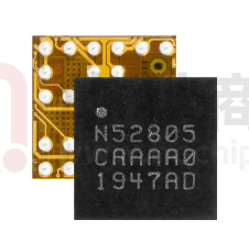


 工商网监
湘ICP备2023018690号
工商网监
湘ICP备2023018690号

