WMQ28N03T1
30V N-Channel Enhancement Mode Power MOSFET
Description
WMQ28N03T1 uses advanced power trench technology that has
been especially tailored to minimize the on-state resistance and
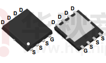
D
D
D
D
D
D
D
yet maintain superior switching performance.
S
S
G
G
Features
S
⚫
PDFN3030-8L
VDS= 30V, ID = 28A
D
S
S
RDS(on) < 18mΩ @ VGS = 10V
RDS(on) < 30mΩ @ VGS = 4.5V
⚫
Green Device Available
⚫
Low Gate Charge
⚫
Advanced High Cell Density Trench Technology
⚫
100% EAS Guaranteed
D
RoHS
compliant
Applications
G
⚫
Power Management Switches
⚫
DC/DC Converter
S
Absolute Maximum Ratings
Parameter
Symbol
Value
Unit
Drain-Source Voltage
VDS
30
V
Gate-Source Voltage
VGS
±20
V
28
TC=25℃
Continuous Drain Current
1
ID
Pulsed Drain Current2
A
18
TC=100℃
IDM
54
A
EAS
12.8
mJ
Avalanche Current
IAS
16
A
Total Power Dissipation4
PD
21
W
TJ, TSTG
-55 to+150
°C
Symbol
Value
Unit
Thermal Resistance from Junction-to-Ambient1
RθJA
74
°C/W
Thermal Resistance from Junction-to-Case1
RθJC
5.95
°C/W
Single Pulse Avalanche Energy3
Operating Junction and Storage Temperature Range
Thermal Characteristics
Parameter
Rev.6.0, 2019
Doc:W0803134
1 / 6
S
�WMQ28N03T1
Electrical Characteristics
Tc = 25°C, unless otherwise noted
Parameter
Symbol
Test Conditions
Min.
Typ.
Max.
Unit
Static Characteristics
Drain-Source Breakdown Voltage
Gate-Body Leakage Current
Zero Gate Voltage Drain
Current
V(BR)DSS
VGS = 0V, ID = 250µA
30
-
-
V
lGSS
VDS = 0V, VGS = ±20V
-
-
±100
nA
-
-
1
IDSS
VDS = 24V, VGS = 0V
-
-
5
1.0
1.75
2.5
VGS = 10V, ID = 10A
-
14
18
VGS = 4.5V, ID = 5A
-
20
30
VDS = 5V, ID = 1A
-
4.6
-
-
500
-
-
75
-
-
51
-
-
2.5
-
-
7.3
-
-
1.5
-
TJ=25℃
TJ=55℃
Gate-Threshold Voltage
VGS(th)
Drain-Source On-Resistance2
RDS(on)
Forward Transconductance2
gfs
VDS = VGS, ID = 250µA
μA
V
mΩ
S
Dynamic Characteristics
Input Capacitance
Ciss
Output Capacitance
Coss
Reverse Transfer Capacitance
Crss
VDS = 15V, VGS =0V, f =1MHz
pF
Switching Characteristics
Rg
Total Gate Charge
Qg
Gate-Source Charge
Qgs
Gate-Drain Charge
Qgd
-
2.3
-
Turn-On Delay Time
td(on)
-
4.2
-
-
9.9
-
-
15.8
-
-
6.2
-
IS = 1A, VGS = 0V
-
-
1.2
V
VG=VD=0V , Force Current
-
-
28
A
Rise Time
Turn-Off Delay Time
Fall Time
tr
td(off)
VDS = 0V, VGS =0V, f =1MHz
Ω
Gate Resistance
VGS = 4.5V, VDS = 20V, ID= 10A
VGS =10V, VDD = 12V,
RG = 3.3Ω, ID= 5A
tf
nC
nS
Drain-source body diode Characteristics
Diode Forward Voltage2
Continuous Source Current1,5
VSD
IS
Note :
1.The data tested by surface mounted on a 1 inch2 FR-4 board with 2OZ copper.
2.The data tested by pulsed , pulse width ≤ 300us , duty cycle ≤ 2%
3.The EAS data shows Max. rating . The test condition is V DD=25V, VGS=10V, L=0.1mH, IAS =16A
4.The power dissipation is limited by 150℃ junction temperature
5.The data is theoretically the same as ID and IDM , in real applications , should be limited by total power dissipation.
Rev.6.0, 2019
www.way-on.com
2 / 6
�WMQ28N03T1
Figure 1. Output Characteristics
Figure 2. Transfer Characteristics
Figure 3. Forward Characteristics of Reverse
Figure 4. Gate Charge Characteristics
Figure 5. RDS(on) vs. VGS
Rev.6.0, 2019
Figure 6. RDS(on) vs. ID
www.way-on.com
3 / 6
�WMQ28N03T1
Figure 7. Capacitance Characteristics
Figure 8. Safe Operating Area
Figure 9. Normalized Maximum Transient Thermal Impedance
Figure 10. Switching Time Waveform
Figure 11. Unclamped Inductive Switching
Waveform
Rev.6.0, 2019
www.way-on.com
4 / 6
�WMQ28N03T1
Mechanical Dimensions for PDFN3030-8L
COMMON DIMENSIONS
MM
SYMBOL
MIN
MAX
A
0.70
0.85
A1
0.10
0.25
D
2.90
3.25
D1
2.25
2.65
E
2.90
3.20
E1
3.10
3.45
E2
1.54
1.98
b
0.20
0.40
e
0.60
0.70
L
0.30
0.50
L1
Rev.6.0, 2019
www.way-on.com
0.13BSC
L2
0.00
0.15
H
0.20
0.65
θ
0°
14°
5 / 6
�WMQ28N03T1
Ordering Information
Part
Package
Marking
Packing method
WMQ28N03T1
PDFN3030-8L
Q28N03
Tape and Reel
Marking Information
Q28N03
WWXX XXX
Q28N03 = Device code
WWXX XXX= Date code
Contact Information
No.1001, Shiwan(7) Road, Pudong District, Shanghai, P.R.China.201207
Tel: 86-21-50310888 Fax: 86-21-50757680 Email: market@way-on.com
WAYON website: http://www.way-on.com
For additional information, please contact your local Sales Representative.
® is registered trademarks of Wayon Corporation.
Disclaimer
WAYON reserves the right to make changes without further notice to any Products herein to improve reliability, function,
or design. The Products are not designed for use in hostile environments, including, without limitation, aircraft, nuclear
power generation, medical appliances, and devices or systems in which malfunction of any Product can reasonably be
expected to result in a personal injury. The information given in this document shall in no event be regarded as a guarantee
of conditions or characteristics. WAYON does not assume any liability for infringement of patents, copyrights, or other
intellectual property rights of third parties by or arising from the use of Products or technical information described in this
document.
Rev.6.0, 2019
www.way-on.com
6 / 6
�


 工商网监
湘ICP备2023018690号
工商网监
湘ICP备2023018690号
